EP4579286A1 - X-ray inspecting device and x-ray inspecting method - Google Patents
X-ray inspecting device and x-ray inspecting method Download PDFInfo
- Publication number
- EP4579286A1 EP4579286A1 EP23857148.3A EP23857148A EP4579286A1 EP 4579286 A1 EP4579286 A1 EP 4579286A1 EP 23857148 A EP23857148 A EP 23857148A EP 4579286 A1 EP4579286 A1 EP 4579286A1
- Authority
- EP
- European Patent Office
- Prior art keywords
- ray
- scintillator
- region
- rays
- inspected object
- Prior art date
- Legal status (The legal status is an assumption and is not a legal conclusion. Google has not performed a legal analysis and makes no representation as to the accuracy of the status listed.)
- Pending
Links
Images



Classifications
-
- G—PHYSICS
- G01—MEASURING; TESTING
- G01N—INVESTIGATING OR ANALYSING MATERIALS BY DETERMINING THEIR CHEMICAL OR PHYSICAL PROPERTIES
- G01N23/00—Investigating or analysing materials by the use of wave or particle radiation, e.g. X-rays or neutrons, not covered by groups G01N3/00 – G01N17/00, G01N21/00 or G01N22/00
- G01N23/02—Investigating or analysing materials by the use of wave or particle radiation, e.g. X-rays or neutrons, not covered by groups G01N3/00 – G01N17/00, G01N21/00 or G01N22/00 by transmitting the radiation through the material
- G01N23/06—Investigating or analysing materials by the use of wave or particle radiation, e.g. X-rays or neutrons, not covered by groups G01N3/00 – G01N17/00, G01N21/00 or G01N22/00 by transmitting the radiation through the material and measuring the absorption
- G01N23/18—Investigating the presence of flaws defects or foreign matter
-
- G—PHYSICS
- G01—MEASURING; TESTING
- G01N—INVESTIGATING OR ANALYSING MATERIALS BY DETERMINING THEIR CHEMICAL OR PHYSICAL PROPERTIES
- G01N23/00—Investigating or analysing materials by the use of wave or particle radiation, e.g. X-rays or neutrons, not covered by groups G01N3/00 – G01N17/00, G01N21/00 or G01N22/00
- G01N23/02—Investigating or analysing materials by the use of wave or particle radiation, e.g. X-rays or neutrons, not covered by groups G01N3/00 – G01N17/00, G01N21/00 or G01N22/00 by transmitting the radiation through the material
- G01N23/04—Investigating or analysing materials by the use of wave or particle radiation, e.g. X-rays or neutrons, not covered by groups G01N3/00 – G01N17/00, G01N21/00 or G01N22/00 by transmitting the radiation through the material and forming images of the material
-
- G—PHYSICS
- G01—MEASURING; TESTING
- G01N—INVESTIGATING OR ANALYSING MATERIALS BY DETERMINING THEIR CHEMICAL OR PHYSICAL PROPERTIES
- G01N23/00—Investigating or analysing materials by the use of wave or particle radiation, e.g. X-rays or neutrons, not covered by groups G01N3/00 – G01N17/00, G01N21/00 or G01N22/00
- G01N23/02—Investigating or analysing materials by the use of wave or particle radiation, e.g. X-rays or neutrons, not covered by groups G01N3/00 – G01N17/00, G01N21/00 or G01N22/00 by transmitting the radiation through the material
- G01N23/06—Investigating or analysing materials by the use of wave or particle radiation, e.g. X-rays or neutrons, not covered by groups G01N3/00 – G01N17/00, G01N21/00 or G01N22/00 by transmitting the radiation through the material and measuring the absorption
- G01N23/083—Investigating or analysing materials by the use of wave or particle radiation, e.g. X-rays or neutrons, not covered by groups G01N3/00 – G01N17/00, G01N21/00 or G01N22/00 by transmitting the radiation through the material and measuring the absorption the radiation being X-rays
-
- G—PHYSICS
- G01—MEASURING; TESTING
- G01T—MEASUREMENT OF NUCLEAR OR X-RADIATION
- G01T1/00—Measuring X-radiation, gamma radiation, corpuscular radiation, or cosmic radiation
- G01T1/16—Measuring radiation intensity
- G01T1/20—Measuring radiation intensity with scintillation detectors
- G01T1/2018—Scintillation-photodiode combinations
-
- G—PHYSICS
- G01—MEASURING; TESTING
- G01N—INVESTIGATING OR ANALYSING MATERIALS BY DETERMINING THEIR CHEMICAL OR PHYSICAL PROPERTIES
- G01N2223/00—Investigating materials by wave or particle radiation
- G01N2223/10—Different kinds of radiation or particles
- G01N2223/101—Different kinds of radiation or particles electromagnetic radiation
- G01N2223/1016—X-ray
-
- G—PHYSICS
- G01—MEASURING; TESTING
- G01N—INVESTIGATING OR ANALYSING MATERIALS BY DETERMINING THEIR CHEMICAL OR PHYSICAL PROPERTIES
- G01N2223/00—Investigating materials by wave or particle radiation
- G01N2223/30—Accessories, mechanical or electrical features
- G01N2223/33—Accessories, mechanical or electrical features scanning, i.e. relative motion for measurement of successive object-parts
- G01N2223/3307—Accessories, mechanical or electrical features scanning, i.e. relative motion for measurement of successive object-parts source and detector fixed; object moves
-
- G—PHYSICS
- G01—MEASURING; TESTING
- G01N—INVESTIGATING OR ANALYSING MATERIALS BY DETERMINING THEIR CHEMICAL OR PHYSICAL PROPERTIES
- G01N2223/00—Investigating materials by wave or particle radiation
- G01N2223/40—Imaging
- G01N2223/401—Imaging image processing
-
- G—PHYSICS
- G01—MEASURING; TESTING
- G01N—INVESTIGATING OR ANALYSING MATERIALS BY DETERMINING THEIR CHEMICAL OR PHYSICAL PROPERTIES
- G01N2223/00—Investigating materials by wave or particle radiation
- G01N2223/50—Detectors
Definitions
- the present invention relates to an X-ray inspection device and an X-ray inspection method.
- the X-ray inspection device described in Patent Literature 1 is a so-called transmission imaging type X-ray inspection device. Specifically, the transmission imaging type X-ray inspection device generates an X-ray image by imaging visible light emitted from a surface of the scintillator opposite to an incident surface on which X-rays are incident.
- the X-ray inspection device described in Patent Literature 2 is a so-called reflection imaging type X-ray inspection device. Specifically, the reflection imaging type X-ray inspection device generates an X-ray image by imaging visible light emitted from an incident surface of the scintillator on which X-rays are incident.
- the present invention has been made in view of the above, and an object thereof is to provide an X-ray inspection device and an X-ray inspection method capable of obtaining an X-ray image suitable for inspection.
- an X-ray inspection device includes: an X-ray emission device configured to emit X-rays toward an inspected object; a scintillator configured to convert the X-rays incident through the inspected object into visible light; and an imaging device configured to image the visible light from the scintillator to generate an X-ray image.
- the scintillator is disposed such that a boundary between an incident surface on which the X-rays are incident and a first side surface intersecting the incident surface is located within an emission range of the X-rays, and the imaging device is arranged so as to face the first side surface, and is configured to image the visible light emitted from a first region of an entire region of the first side surface, the entire region of the first side surface being divided into two regions of the first region including the boundary and a second region excluding the first region.
- the X-ray inspection device further includes an X-ray shielding member that is disposed between the inspected object and the scintillator and is configured to shield the X-rays incident on a fourth region of an entire region of the incident surface, the entire region of the incident surface being divided into two regions of a third region including the boundary and the fourth region excluding the third region.
- a dimension between the first side surface and a second side surface opposite to the first side surface is set to 30 ⁇ m or more and 500 ⁇ m or less.
- the X-ray inspection device further includes an image analysis device configured to analyze the X-ray image.
- the image analysis device is configured to estimate a feature amount of an abnormal part present in the inspected object based on a luminance distribution of the visible light along an incident direction of the X-rays in the X-ray image.
- the X-ray emission device and the scintillator are installed such that a width of a penumbra represented by (L2 - L1) ⁇ R/L1 is 30 ⁇ m or less, a distance from an X-ray focal point of the X-ray emission device to the inspected object being L1 [mm], a distance from the X-ray focal point to the scintillator being L2 [mm], a diameter of the X-ray focal point being R [ ⁇ m].
- the X-ray inspection device further includes a transfer device configured to move the inspected object relative to the X-ray emission device, the scintillator, and the imaging device in a direction substantially perpendicular to the first side surface, or repeat the relative movement and stopping.
- An X-ray inspection method includes: a scintillator disposing step of disposing a scintillator such that a boundary between an incident surface of the scintillator on which X-rays are incident and a first side surface intersecting the incident surface is located within an emission range of the X-rays; an imaging device disposing step of disposing an imaging device so as to face the first side surface; an X-ray emission step of emitting the X-rays from an X emission device toward an inspected object; and an imaging step of, by the imaging device, imaging visible light to generate an X-ray image, the visible light being converted from the X-rays, which are incident on the scintillator via the inspected object, by the scintillator.
- the visible light emitted from a first region of an entire region of the first side surface is imaged by the imaging device, the entire region of the first side surface being divided into two regions of the first region including the boundary and a second region excluding the first region.
- the X-ray inspection method further includes an X-ray shielding member disposing step of disposing an X-ray shielding member configured to shield the X-rays between the inspected object and the scintillator to shield the X-rays incident on a fourth region, an entire region of the incident surface being divided into two regions of a third region including the boundary and the fourth region excluding the third region.
- the X-ray inspection method further includes an image analysis step of analyzing the X-ray image.
- image analysis step a feature amount of an abnormal part present in the inspected object is estimated on the basis of a luminance distribution of the visible light along an incident direction of the X-rays in the X-ray image.
- the X-ray inspection method further includes a positional relationship adjustment step of adjusting a positional relationship between the X-ray emission device and the scintillator.
- a positional relationship between the X-ray emission device and the scintillator is adjusted such that a width of a penumbra represented by (L2 - L1) ⁇ R/L1 is 1/6 or less of a diameter of a defect to be detected with respect to the inspected object, a distance from an X-ray focal point of the X-ray emission device to the inspected object being L1 [mm], a distance from the X-ray focal point to the scintillator being L2 [mm], a diameter of the X-ray focal point being R [ ⁇ m].
- the X-ray inspection method according to the present invention further includes a transfer step of moving the inspected object relative to the X-ray emission device, the scintillator, and the imaging device in a direction substantially perpendicular to the first side surface, or repeating the relative movement and stopping.
Landscapes
- Health & Medical Sciences (AREA)
- General Physics & Mathematics (AREA)
- Physics & Mathematics (AREA)
- Life Sciences & Earth Sciences (AREA)
- Chemical & Material Sciences (AREA)
- Analytical Chemistry (AREA)
- Biochemistry (AREA)
- General Health & Medical Sciences (AREA)
- Immunology (AREA)
- Pathology (AREA)
- Toxicology (AREA)
- High Energy & Nuclear Physics (AREA)
- Molecular Biology (AREA)
- Spectroscopy & Molecular Physics (AREA)
- Analysing Materials By The Use Of Radiation (AREA)
- Measurement Of Radiation (AREA)
Abstract
Description
- The present invention relates to an X-ray inspection device and an X-ray inspection method. Background
- Conventionally, there has been known an X-ray inspection device that emits X-rays to an inspected object, converts the X-rays passing through the inspected object into visible light by a scintillator (emits fluorescence by the X-rays and emits visible light), and images the visible light by an imaging device to generate an X-ray image (see, for example, Patent Literatures 1 and 2).
- The X-ray inspection device described in Patent Literature 1 is a so-called transmission imaging type X-ray inspection device. Specifically, the transmission imaging type X-ray inspection device generates an X-ray image by imaging visible light emitted from a surface of the scintillator opposite to an incident surface on which X-rays are incident.
- The X-ray inspection device described in
Patent Literature 2 is a so-called reflection imaging type X-ray inspection device. Specifically, the reflection imaging type X-ray inspection device generates an X-ray image by imaging visible light emitted from an incident surface of the scintillator on which X-rays are incident. -
- Patent Literature 1:
JP H01-262451 A - Patent Literature 2:
JP 2020-160079 A - However, in the transmission imaging type X-ray inspection device described in Patent Literature 1, when the X-rays are incident on the scintillator, the visible light converted by the scintillator travels inside the scintillator and is absorbed inside the scintillator. Therefore, the luminance of the visible light emitted from the surface opposite to the incident surface is low, and a dark X-ray image is obtained. In addition, when a particle type scintillator is employed, visible light traveling inside the scintillator is likely to scatter inside the scintillator. Therefore, an unclear X-ray image is obtained
- That is, in the transmission imaging type X-ray inspection device described in Patent Literature 1, there is a problem that a dark or unclear X-ray image is obtained, and it is difficult to obtain an X-ray image suitable for inspection.
- Furthermore, in the reflection imaging type X-ray inspection device described in
Patent Literature 2, it is necessary to advance the visible light emitted from the incident surface of the scintillator on which X-rays are incident toward the imaging device, and thus it is necessary to tilt the scintillator with respect to the inspected object. Therefore, the distance between the inspected object and the scintillator becomes relatively large. As a result, blur (penumbra) occurring in the X-ray image becomes large, and an unclear X-ray image is obtained. - That is, in the reflection imaging type X-ray inspection device described in
Patent Literature 2, there is a problem that an unclear X-ray image is obtained, and it is difficult to obtain an X-ray image suitable for inspection. - Against this background, there is a demand for a technique capable of obtaining an X-ray image suitable for inspection.
- The present invention has been made in view of the above, and an object thereof is to provide an X-ray inspection device and an X-ray inspection method capable of obtaining an X-ray image suitable for inspection.
- To solve the problem described above and to achieve the object, an X-ray inspection device according to the present invention includes: an X-ray emission device configured to emit X-rays toward an inspected object; a scintillator configured to convert the X-rays incident through the inspected object into visible light; and an imaging device configured to image the visible light from the scintillator to generate an X-ray image. The scintillator is disposed such that a boundary between an incident surface on which the X-rays are incident and a first side surface intersecting the incident surface is located within an emission range of the X-rays, and the imaging device is arranged so as to face the first side surface, and is configured to image the visible light emitted from a first region of an entire region of the first side surface, the entire region of the first side surface being divided into two regions of the first region including the boundary and a second region excluding the first region.
- The X-ray inspection device according to the present invention further includes an X-ray shielding member that is disposed between the inspected object and the scintillator and is configured to shield the X-rays incident on a fourth region of an entire region of the incident surface, the entire region of the incident surface being divided into two regions of a third region including the boundary and the fourth region excluding the third region.
- In the scintillator of the X-ray inspection device according to the present invention, a dimension between the first side surface and a second side surface opposite to the first side surface is set to 30 µm or more and 500 µm or less.
- The X-ray inspection device according to the present invention further includes an image analysis device configured to analyze the X-ray image. The image analysis device is configured to estimate a feature amount of an abnormal part present in the inspected object based on a luminance distribution of the visible light along an incident direction of the X-rays in the X-ray image.
- In the X-ray inspection device according to the present invention, the X-ray emission device and the scintillator are installed such that a width of a penumbra represented by (L2 - L1) × R/L1 is 30 µm or less, a distance from an X-ray focal point of the X-ray emission device to the inspected object being L1 [mm], a distance from the X-ray focal point to the scintillator being L2 [mm], a diameter of the X-ray focal point being R [µm].
- The X-ray inspection device according to the present invention further includes a transfer device configured to move the inspected object relative to the X-ray emission device, the scintillator, and the imaging device in a direction substantially perpendicular to the first side surface, or repeat the relative movement and stopping.
- An X-ray inspection method according to the present invention includes: a scintillator disposing step of disposing a scintillator such that a boundary between an incident surface of the scintillator on which X-rays are incident and a first side surface intersecting the incident surface is located within an emission range of the X-rays; an imaging device disposing step of disposing an imaging device so as to face the first side surface; an X-ray emission step of emitting the X-rays from an X emission device toward an inspected object; and an imaging step of, by the imaging device, imaging visible light to generate an X-ray image, the visible light being converted from the X-rays, which are incident on the scintillator via the inspected object, by the scintillator. In the imaging step, the visible light emitted from a first region of an entire region of the first side surface is imaged by the imaging device, the entire region of the first side surface being divided into two regions of the first region including the boundary and a second region excluding the first region.
- The X-ray inspection method according to the present invention further includes an X-ray shielding member disposing step of disposing an X-ray shielding member configured to shield the X-rays between the inspected object and the scintillator to shield the X-rays incident on a fourth region, an entire region of the incident surface being divided into two regions of a third region including the boundary and the fourth region excluding the third region.
- The X-ray inspection method according to the present invention further includes an image analysis step of analyzing the X-ray image. In the image analysis step, a feature amount of an abnormal part present in the inspected object is estimated on the basis of a luminance distribution of the visible light along an incident direction of the X-rays in the X-ray image.
- The X-ray inspection method according to the present invention further includes a positional relationship adjustment step of adjusting a positional relationship between the X-ray emission device and the scintillator. In the positional relationship adjustment step, a positional relationship between the X-ray emission device and the scintillator is adjusted such that a width of a penumbra represented by (L2 - L1) × R/L1 is 1/6 or less of a diameter of a defect to be detected with respect to the inspected object, a distance from an X-ray focal point of the X-ray emission device to the inspected object being L1 [mm], a distance from the X-ray focal point to the scintillator being L2 [mm], a diameter of the X-ray focal point being R [µm].
- The X-ray inspection method according to the present invention further includes a transfer step of moving the inspected object relative to the X-ray emission device, the scintillator, and the imaging device in a direction substantially perpendicular to the first side surface, or repeating the relative movement and stopping. Advantageous Effects of Invention
- According to the X-ray inspection device and the X-ray inspection method of the present invention, an X-ray image suitable for inspection can be obtained.
-
-
FIG. 1 is a diagram illustrating an X-ray inspection device according to a first embodiment. -
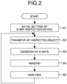
FIG. 2 is a flowchart illustrating an X-ray inspection method. -
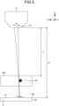
FIG. 3 is a diagram for describing Step S1. -
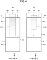
FIG. 4 is a diagram for describing Step S5. -
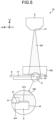
FIG. 5 is a diagram illustrating an X-ray inspection device according to a second embodiment. -
FIG. 6 is a diagram illustrating an effect of the second embodiment. -
FIG. 7 is a diagram illustrating an X-ray inspection device according to a third embodiment. -
FIG. 8 is a diagram illustrating an effect of the third embodiment. -
FIG. 9 is a diagram for describing a modification of the first to third embodiments. - Hereinafter, modes for carrying out the present invention (hereinafter referred to as embodiments) will be described with reference to the drawings. Note that the present invention is not limited by the embodiments described below. Furthermore, in the description of the drawings, the same parts are denoted by the same reference numerals.
-
FIG. 1 is a diagram illustrating an X-ray inspection device 1 according to a first embodiment. - The X-ray inspection device 1 emits X-rays to an inspected object OB (
FIG. 1 ) such as a film or a fiber, converts the X-rays transmitted through the inspected object OB into visible light, and captures the visible light to generate an X-ray image. Then, the X-ray inspection device 1 analyzes the X-ray image to estimate the feature amount of a defect DE (seeFIG. 3 ) such as a metal foreign substance in the inspected object OB. - Note that the inspected object OB is not limited to a film or a fiber, but may be a paper, a resin, an integrated circuit, or the like.
- As illustrated in
FIG. 1 , the X-ray inspection device 1 includes anX-ray emission device 2, a transfer device 3, ascintillator 4, animaging device 5, a display device 6, and acontrol device 7. - Note that in the following description of the configuration of the X-ray inspection device 1, an axis along the vertical direction is defined as a Z axis, and two axes orthogonal to the Z axis are defined as an X axis and a Y axis. In
FIG. 1 , the Z axis is an axis along the up-down direction. The X axis is an axis along the left-right direction. Furthermore, the Y axis is an axis orthogonal to the paper surface ofFIG. 1 . - The
X-ray emission device 2 emits a conical X-ray beam (cone beam) from an X-ray focal point 21 (FIG. 1 ) toward the inspected object OB under the control of thecontrol device 7. InFIG. 1 , an emission range SP of the conical X-ray beam is expressed by dots. In the first embodiment, the emission direction of X-rays from theX-ray emission device 2 is the -Z-axis direction (downward inFIG. 1 ). - Note that the
X-ray emission device 2 may be a closed type or an open type, and may be a millifocus type or a microfocus type. - The transfer device 3 includes a transfer roller, a belt conveyor, and the like, and transfers the inspected object OB while holding the inspected object OB under the control of the
control device 7. In the first embodiment, the transfer direction of the inspected object OB is the - X-axis direction (rightward inFIG. 1 ). The -X axis direction is a direction substantially perpendicular to afirst side surface 42 described later. - As illustrated in
FIG. 1 , thescintillator 4 is formed of a plate body having a rectangular shape in plane view, and is disposed on the -Z axis side of the inspected object OB with the plate surface substantially parallel to the XY plane. Then, thescintillator 4 converts the X-rays incident after passing through the inspected object OB into visible light (fluorescence emission by the X-ray). - Here, in the
scintillator 4, the X-rays transmitted through the inspected object OB are incident on the plate surface on the +Z axis side (upper side inFIG. 1 ), the plate surface corresponding to an incident surface 41 (FIG. 1 ) according to the present invention. In thescintillator 4, the side surface on the -X axis side intersects theincident surface 41 and corresponds to the first side surface 42 (FIG. 1 ) according to the present invention. - Note that the
scintillator 4 may be of a particle type or a single crystal type. - The
imaging device 5 includes an imaging element such as a charge coupled device (CCD) or a complementary metal oxide semiconductor (CMOS) that receives incident light and converts the light into an electric signal, and is a camera that captures visible light from thescintillator 4 to generate an X-ray image. Then, theimaging device 5 outputs the generated X-ray image data to thecontrol device 7. - Note that the
imaging device 5 may be a line sensor camera, an area sensor camera, or a time delay integration type camera. - The display device 6 includes a display using liquid crystal, organic electro luminescence (EL), or the like, and displays various images such as an X-ray image under the control of the
control device 7. - The
control device 7 integrally controls the entire operation of the X-ray inspection device 1. As illustrated inFIG. 1 , thecontrol device 7 includes aprocessor 71, a storage unit 72, and an input unit 73. - The
processor 71 is implemented by executing various programs stored in the storage unit 72 by a controller such as a central processing unit (CPU) or a micro processing unit (MPU), and controls the entire operation of the X-ray inspection device 1. - Note that the
processor 71 is not limited to a CPU or an MPU, and may be configured by an integrated circuit such as an application specific integrated circuit (ASIC) or a field-programmable gate array (FPGA). The function of theprocessor 71 will be described in "X-ray inspection method" described later. - In addition to various programs executed by the
processor 71, the storage unit 72 stores data and the like necessary for theprocessor 71 to perform processing. - The input unit 73 includes a button, a switch, a touch panel, and the like that receive a user operation by an operator, and outputs an operation signal corresponding to the user operation to the
processor 71. Note that part or all of the functions of the input unit 73 may be arranged on the display screen of the display device 6 as a touch panel. - Next, an X-ray inspection method using the above-described X-ray inspection device 1 will be described.
-
FIG. 2 is a flowchart illustrating the X-ray inspection method. - First, the operator performs initial setting of the X-ray inspection device 1 (Step S1).
-
FIG. 3 is a diagram illustrating Step S1. Specifically,FIG. 3 is a diagram illustrating a positional relationship among theX-ray emission device 2, the inspected object OB, and thescintillator 4. InFIG. 3 , reference sign "R" is a diameter [µm] of the X-rayfocal point 21. Reference sign "L1" is a distance [mm] from the X-rayfocal point 21 to the inspected object OB. Furthermore, reference sign "L2" is a distance [mm] from the X-rayfocal point 21 to thescintillator 4. Reference sign "r" is a width [µm] of a penumbra (blur) SH. - Here, the penumbra SH in X-ray inspection will be described.
- In X-ray inspection, when the distance (L2 - L1) from the inspected object OB to the
scintillator 4 is increased and the shadow of the defect DE such as metal foreign matter in the inspected object OB due to the emitted X-rays is geometrically increased, the detection sensitivity of the minute defect DE becomes low. - Specifically, the X-ray
focal point 21 has a finite diameter R [µm]. For this reason, X-rays enter the region that should be a shadow of the defect DE, and the penumbra SH (FIG. 3 ) is generated. That is, since the penumbra SH is generated in the portion that should be a shadow of the defect DE, it is difficult to detect the defect DE with high accuracy. - The penumbra SH occurs at both ends of the defect DE. Therefore, the shadow of the defect DE is smaller than the original shadow by 2×r. Here, the width r of the penumbra SH is represented by (L2 - L1) × R/L1.
- As a result of intensive studies, the inventor of the present application has found that it is necessary to set the width r of the penumbra SH to 1/6 or less of the diameter of the defect DE in order to reliably detect the defect DE. In the first embodiment, the diameter of the defect DE is 30 µm or more and 200 µm or less.
- Then, in Step S1, the operator sets the diameter of the defect DE to be detected with respect to the inspected object OB to about 180 µm, and adjusts the distances L1 and L2 so that the width r of the penumbra SH is 1/6 (30 µm) or less of the 180 µm.
- In Step S1, the operator disposes the
scintillator 4 such that a boundary BO (FIG. 1 ) between theincident surface 41 and thefirst side surface 42 in thescintillator 4 is located within the X-ray emission range SP. - Furthermore, in Step S1, the worker disposes the
imaging device 5 so as to face thefirst side surface 42. - As described above, Step S1 corresponds to a positional relationship adjustment step, a scintillator disposing step, and an imaging device disposing step according to the present invention.
- After Step S1, the operator performs an operation of starting the X-ray inspection on the input unit 73. Accordingly, the
processor 71 executes the following processing. - First, the
processor 71 operates the transfer device 3 to transfer the inspected object OB at a predetermined speed (Step S2: transfer step). - After Step S2, the
processor 71 operates theX-ray emission device 2. Then, theX-ray emission device 2 emits X-rays toward the inspected object OB (Step S3: X-ray emission step). - After Step S3, the
processor 71 operates theimaging device 5. Then, theimaging device 5 images visible light to generate an X-ray image, the visible light being converted from X-rays, which are incident on thescintillator 4 via the inspected object OB, by the scintillator 4 (Step S4: imaging step). Theimaging device 5 outputs the generated X-ray image data to thecontrol device 7. - Here, assume that the entire region of the
first side surface 42 is divided into two regions of a first region Ar1 (seeFIG. 4 ) including the boundary BO and a second region Ar2 (seeFIG. 4 ) excluding the first region Ar1. In this case, in Step S4, the visible light emitted from the first region Ar1 of the entire region of thefirst side surface 42 is imaged by theimaging device 5. That is, in Step S4, the visible light emitted from the region (first region Ar1) in the vicinity of the boundary BO among the entire region of thefirst side surface 42 is imaged by theimaging device 5. - After Step S4, the
processor 71 acquires data of the X-ray image generated in Step S4 from theimaging device 5, and analyzes the X-ray image (Step S5: image analysis step). Thereafter, theprocessor 71 returns to Step S2. -
FIG. 4 is a diagram illustrating Step S5. Specifically, (a) ofFIG. 4 illustrates an X-ray image F1 when the thickness of the defect DE in the inspected object OB is large or when the density of the defect DE is high. Meanwhile, (b) ofFIG. 4 illustrates an X-ray image F2 when the thickness of the defect DE in the inspected object OB is small or when the density of the defect DE is low. Note that InFIG. 4 , the density of dots is increased as the luminance of the visible light converted from the X-rays is lower in regions ArS1 and ArS2 that become the shadow of the defect DE by the X-rays. Furthermore, inFIG. 4 , for convenience of description, on thefirst side surface 42, regions other than the regions ArS1 and ArS2 are not denoted by dots. - Incidentally, when the defect DE is in the inspected object OB, as illustrated in
FIG. 4 , the X-rays are absorbed by the defect DE, and the regions ArS1 and ArS2 that become shadows of the defect DE are generated. In the regions ArS1 and ArS2, in regions close to theincident surface 41, the luminance of the visible light converted from the X-rays is low due to absorption of the X-rays by the defect DE. Then, in the regions ArS1 and ArS2, the luminance of the visible light gradually increases toward the -Z direction due to the influence of the visible light from regions other than the regions ArS1 and ArS2, and finally becomes substantially the same as the luminance of the visible light in the regions other than the regions ArS1 and ArS2. - Here, as can be seen by comparing (a) of
FIG. 4 with (b) ofFIG. 4 , when the thickness and density of the defect DE are different, the luminance distribution of the visible light along the Z-axis direction such as the lengths of the regions ArS1 and ArS2 in the Z-axis direction is different. Specifically, the length of the region ArS1 in the Z-axis direction is longer than the length of the region ArS2 in the Z-axis direction. That is, there is a correlation between the feature amount such as the thickness and density of the defect DE and the luminance distribution of visible light along the Z-axis direction (incident direction of X-rays) in the X-ray image. Then, the storage unit 72 stores correlation information indicating the correlation. - Note that the luminance distribution of visible light along the Z-axis direction also depends on the length of the defect DE in the Y-axis direction. Therefore, the feature amount constituting the correlation information stored in the storage unit 72 may include the length of the defect DE in the Y-axis direction in addition to the thickness and density of the defect DE.
- In Step S5, the
processor 71 acquires the luminance distribution (light reception amount profile) of visible light along the Z-axis direction from the X-ray image generated in Step S4, refers to the correlation information stored in the storage unit 72, and estimates the feature amount corresponding to the luminance distribution. That is, thecontrol device 7 corresponds to an image analysis device according to the present invention. - Here, the length of the
scintillator 4 in the Z-axis direction (up-down direction inFIG. 4 ) is preferably 200 µm or more in order to acquire the light reception amount profile in Step S5. Thescintillator 4 has a length of about 60 to 100 mm in the Y-axis direction (left-right direction inFIG. 4 ). - According to the first embodiment described above, the following effects are obtained.
- In the X-ray inspection device 1 according to the first embodiment, the
scintillator 4 is disposed such that the boundary BO is located within the X-ray emission range SP. Moreover, theimaging device 5 is disposed so as to face thefirst side surface 42, and images visible light emitted from the first region Ar1 including the boundary BO among the entire region of thefirst side surface 42. - That is, the
imaging device 5 does not image visible light transmitted through the scintillator as in the transmission imaging type X-ray inspection device described in Patent Literature 1, but images visible light emitted from the first region Ar1 on thefirst side surface 42. In other words, theimaging device 5 images visible light with less influence of absorption and scattering inside thescintillator 4. Therefore, a bright and clear X-ray image can be generated. - In addition, since it is not necessary to tilt the scintillator with respect to the inspected object as in the reflection imaging type X-ray inspection device described in
Patent Literature 2, thescintillator 4 can be brought close to the inspected object OB. Therefore, the width r of the penumbra SH generated in the X-ray image can be reduced, and a clear X-ray image can be generated. - As described above, according to the X-ray inspection device 1 of the first embodiment, an X-ray image suitable for inspection can be obtained.
- Incidentally, in the reflection imaging type X-ray inspection device described in
Patent Literature 2, the imaging device needs to image the incident surface of the scintillator. For this reason, the inspected object enters the imaging visual field of the imaging device, the incident surface of the scintillator is easily blocked by the inspected object, and it is difficult to set the installation position of the imaging device. - On the other hand, in the X-ray inspection device 1 according to the first embodiment, the
imaging device 5 is disposed so as to face thefirst side surface 42, and images the visible light emitted from the first region Ar1 on thefirst side surface 42. Therefore, the first region Ar1 is not blocked by the inspected object, and theimaging device 5 can be easily installed. In addition, by installing theimaging device 5 so as to face thefirst side surface 42, theimaging device 5 is not exposed to X-rays. Therefore, the life of theimaging device 5 can be prolonged. - Moreover, in the X-ray inspection device 1 according to the first embodiment, the
X-ray emission device 2 and thescintillator 4 are installed such that the width r of the penumbra SH is 1/6 (30 µm) or less of 180 µm that is the diameter of the defect DE to be detected with respect to the inspected object OB. - Therefore, the defect DE can be reliably detected.
- In the X-ray inspection device 1 of the first embodiment, the
processor 71 estimates the feature amount of the defect DE existing in the inspected object OB on the basis of the luminance distribution (light reception amount profile) of visible light along the incident direction of the X-rays in the X-ray images F1 and F2. - Therefore, the feature amount (thickness and density) of the defect DE can be easily estimated by simple processing.
- Next, a second embodiment will be described.
- In the following description, the same reference numerals are given to the same configurations as those of the above-described first embodiment, and detailed descriptions thereof will be omitted or simplified.
-
FIG. 5 is a diagram corresponding toFIG. 1 , and is a diagram illustrating anX-ray inspection device 1A according to the second embodiment. Note that inFIG. 5 , for convenience of description, illustration of a transfer device 3, animaging device 5, a display device 6, and acontrol device 7 is omitted. - In the
X-ray inspection device 1A according to the second embodiment, as illustrated inFIG. 5 , anX-ray shielding member 8 is added to the X-ray inspection device 1 described in the first embodiment. - The
X-ray shielding member 8 is a plate body that is made of, for example, aluminum, iron, or the like and shields X-rays. Then, as illustrated inFIG. 5 , theX-ray shielding member 8 is disposed between an inspected object OB and ascintillator 4, and shields X-rays incident on a partial region of the entire region of anincident surface 41. - In an X-ray inspection method according to the second embodiment, the
X-ray shielding member 8 is disposed in Step S1 in the X-ray inspection method described in the first embodiment. - Here, assume that the entire region of the
incident surface 41 is divided into two regions of a third region Ar3 (FIG. 5 ) including a boundary BO and a fourth region Ar4 (FIG. 5 ) excluding the third region Ar3. In this case, in Step S1, the operator disposes theX-ray shielding member 8 between the inspected object OB and thescintillator 4 in order to shield the X-rays incident on the fourth region Ar4. - That is, Step S1 corresponds to an X-ray shielding member disposing step in addition to a positional relationship adjustment step, the scintillator disposing step, and the imaging device disposing step according to the present invention.
- The length in the X-axis direction (left-right direction in
FIG. 5 ) in the third region Ar3 is preferably 30 µm or more and 500 µm or less in consideration of the diameter of a defect DE. - According to the second embodiment described above, the following effects are obtained in addition to the same effects as those of the first embodiment described above.
-
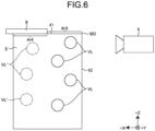
FIG. 6 is a diagram illustrating an effect of the second embodiment. Specifically,FIG. 6 illustrates a positional relationship among theX-ray shielding member 8, thescintillator 4, and theimaging device 5. Note that inFIG. 6 , a circle indicated by a reference sign "VL" represents visible light converted from X-rays by thescintillator 4. - For example, as the visible light of the regions ArS1 and ArS2 described above, in addition to the visible light VL (represented by solid circle in
FIG. 6 ) obtained by converting the X-rays transmitted through the defect DE by thescintillator 4, assume a case where visible light VL' (represented by alternate long and short dash line circle inFIG. 6 ) obtained by converting the X-rays not transmitted through the defect DE by thescintillator 4 is included. In this case, the luminance of the visible light VL is buried by the luminance of the visible light VL', and it is difficult to estimate the feature amount of the defect DE with high accuracy. - Therefore, the
X-ray inspection device 1A according to the second embodiment further includes theX-ray shielding member 8 that shields the X-ray incident on the fourth region Ar4 among the entire region of theincident surface 41. That is, generation of the visible light VL' is prevented by disposing theX-ray shielding member 8. Therefore, the feature amount of the defect DE can be estimated with high accuracy. - Next, a third embodiment will be described.
- In the following description, the same reference numerals are given to the same configurations as those of the above-described first embodiment, and detailed descriptions thereof will be omitted or simplified.
-
FIG. 7 is a diagram corresponding toFIG. 1 , and is a diagram illustrating anX-ray inspection device 1B according to the third embodiment. Note that inFIG. 7 , for convenience of description, illustration of a transfer device 3, animaging device 5, a display device 6, and acontrol device 7 is omitted. - In the
X-ray inspection device 1B according to the third embodiment, as illustrated inFIG. 6 , ascintillator 4B having a shape different from that of thescintillator 4 is adopted in the X-ray inspection device 1 described in the first embodiment. - As illustrated in
FIG. 7 , thescintillator 4B is formed of a plate body having a rectangular shape in plane view, and is disposed on the -Z axis side of an inspected object OB with the plate surface substantially parallel to the XZ plane. - Here, in the
scintillator 4B, the X-rays transmitted through the inspected object OB are incident on the end face on the +Z axis side (upper side inFIG. 7 ), the end face corresponding to anincident surface 41B according to the present invention. In thescintillator 4B, a plate surface on the -X axis side (right side inFIG. 7 ) intersects theincident surface 41B and corresponds to afirst side surface 42B according to the present invention. Furthermore, in thescintillator 4B, the plate surface on the +X axis side (left side inFIG. 7 ) is opposite to thefirst side surface 42B, and corresponds to asecond side surface 43B according to the present invention. - An X-ray inspection method according to the third embodiment is the same as the X-ray inspection method described in the first embodiment.
- That is, in Step S1, as described in the aforementioned first embodiment, the operator disposes the
scintillator 4B such that a boundary BO (FIG. 7 ) between theincident surface 41B and thefirst side surface 42B in thescintillator 4B is located within the X-ray emission range SP (FIG. 7 ). - Here, the thickness between the first and second side surfaces 42B and 43B in the
scintillator 4B is preferably 30 µm or more and 500 µm or less in consideration of the diameter of a defect DE. In addition, the length of thescintillator 4B in the Z-axis direction (up-down direction inFIG. 7 ) is preferably 200 µm or more in order to acquire the light reception amount profile in Step S5. Furthermore, the length of thescintillator 4B in the Y-axis direction (direction orthogonal to paper surface ofFIG. 7 ) is about 60 to 100 mm. - According to the third embodiment described above, the following effects are obtained in addition to the same effects as those of the first embodiment described above.
-
FIG. 8 is a diagram illustrating an effect of the third embodiment. Specifically,FIG. 8 illustrates a positional relationship between thescintillator 4B and theimaging device 5. InFIG. 8 , a circle indicated by a reference sign "VL" represents visible light converted from X-rays by thescintillator 4B, as inFIG. 6 . - In the
X-ray inspection device 1B according to the third embodiment, thescintillator 4B has a thickness between the first and second side surfaces 42B and 43B set to 30 µm or more and 500 µm or less. - For this reason, it is possible to prevent the occurrence of visible light VL' (represented by alternate long and short dash line circle in
FIG. 8 ) in which the X-rays not transmitted through the defect DE are converted by thescintillator 4B, and to configure the visible light of the regions ArS1 and ArS2 described above by the visible light VL (represented by solid circle inFIG. 8 ) in which the X-rays transmitted through the defect DE are converted by thescintillator 4B. Therefore, as in the second embodiment described above, the feature amount of the defect DE can be estimated with high accuracy. - While embodiments for carrying out the present invention have been described so far, the present invention should not be limited only by the above-described first to third embodiments.
- In the above-described first to third embodiments, imaging is performed by the
imaging device 5 while the inspected object OB is transferred, but the present invention is not limited thereto. In the transfer step S2, the transfer device 3 may temporarily stop the transfer of the inspected object OB when imaging is performed by theimaging device 5. - In the above-described first to third embodiments, the transfer device 3 transfers (moves) the inspected object OB in the transfer step S2, but the present invention is not limited thereto. In the transfer step S2, the transfer device 3 only needs to move the inspected object OB relative to the
X-ray emission device 2, the scintillator 4 (4B), and theimaging device 5 in a direction substantially perpendicular to thefirst side surface 42. Hence, theX-ray emission device 2, the scintillator 4 (4B), and theimaging device 5 may be moved without moving the inspected object OB. -
FIG. 9 is a diagram illustrating a modification of the first to third embodiments. - In the first to third embodiments described above, in the scintillator 4 (4B), as illustrated in (a) of
FIG. 9 , theincident surface 41 and thefirst side surface 42 intersect each other so as to be orthogonal to each other, but the present invention is not limited thereto. For example, as illustrated in (b) ofFIG. 9 , theincident surface 41 and thefirst side surface 42 may intersect at an obtuse angle. In addition, for example, as illustrated in (c) ofFIG. 9 , a corner between theincident surface 41 and thefirst side surface 42 may be chamfered. Furthermore, for example, as illustrated in (d) ofFIG. 9 , a corner between theincident surface 41 and thefirst side surface 42 may be rounded. -
- 1,1A,1B X-RAY INSPECTION DEVICE
- 2 X-RAY EMISSION DEVICE
- 3 TRANSFER DEVICE
- 4,4B SCINTILLATOR
- 5 IMAGING DEVICE
- 6 DISPLAY DEVICE
- 7 CONTROL DEVICE
- 8 X-RAY SHIELDING MEMBER
- 21 X-RAY FOCAL POINT
- 41,41B INCIDENT SURFACE
- 42,42B FIRST SIDE SURFACE
- 43B SECOND SIDE SURFACE
- 71 PROCESSOR
- 72 STORAGE UNIT
- 73 INPUT UNIT
- Ar1 FIRST REGION
- Ar2 SECOND REGION
- Ar3 THIRD REGION
- Ar4 FOURTH REGION
- ArS1,ArS2 REGION
- BO BOUNDARY
- DE DEFECT
- F1,F2 X-RAY IMAGE
- L1,L2 DISTANCE
- OB OBJECT
- r WIDTH
- SH PENUMBRA
- SP EMISSION RANGE
- VL,VL' VISIBLE LIGHT
Claims (11)
- An X-ray inspection device comprising:an X-ray emission device configured to emit X-rays toward an inspected object;a scintillator configured to convert the X-rays incident through the inspected object into visible light; andan imaging device configured to image the visible light from the scintillator to generate an X-ray image, whereinthe scintillator is disposed such that a boundary between an incident surface on which the X-rays are incident and a first side surface intersecting the incident surface is located within an emission range of the X-rays, andthe imaging device is arranged so as to face the first side surface, and is configured to image the visible light emitted from a first region of an entire region of the first side surface, the entire region of the first side surface being divided into two regions of the first region including the boundary and a second region excluding the first region.
- The X-ray inspection device according to claim 1, further comprising an X-ray shielding member that is disposed between the inspected object and the scintillator and is configured to shield the X-rays incident on a fourth region of an entire region of the incident surface, the entire region of the incident surface being divided into two regions of a third region including the boundary and the fourth region excluding the third region.
- The X-ray inspection device according to claim 1, wherein
in the scintillator, a dimension between the first side surface and a second side surface opposite to the first side surface is set to 30 µm or more and 500 µm or less. - The X-ray inspection device according to claim 1, further comprisingan image analysis device configured to analyze the X-ray image, whereinthe image analysis device is configured to estimate a feature amount of an abnormal part present in the inspected object based on a luminance distribution of the visible light along an incident direction of the X-rays in the X-ray image.
- The X-ray inspection device according to claim 1, wherein
the X-ray emission device and the scintillator are installed such that a width of a penumbra represented by (L2 - L1) × R/L1 is 30 µm or less, a distance from an X-ray focal point of the X-ray emission device to the inspected object being L1 [mm], a distance from the X-ray focal point to the scintillator being L2 [mm], a diameter of the X-ray focal point being R [µm]. - The X-ray inspection device according to claim 1, further comprising a transfer device configured to move the inspected object relative to the X-ray emission device, the scintillator, and the imaging device in a direction substantially perpendicular to the first side surface, or repeat the relative movement and stopping.
- An X-ray inspection method comprising:a scintillator disposing step of disposing a scintillator such that a boundary between an incident surface of the scintillator on which X-rays are incident and a first side surface intersecting the incident surface is located within an emission range of the X-rays;an imaging device disposing step of disposing an imaging device so as to face the first side surface;an X-ray emission step of emitting the X-rays from an X-ray emission device toward an inspected object; andan imaging step of, by the imaging device, imaging visible light to generate an X-ray image, the visible light being converted from the X-rays, which are incident on the scintillator via the inspected object, by the scintillator, whereinin the imaging step, the visible light emitted from a first region of an entire region of the first side surface is imaged by the imaging device, the entire region of the first side surface being divided into two regions of the first region including the boundary and a second region excluding the first region.
- The X-ray inspection method according to claim 7, further comprising an X-ray shielding member disposing step of disposing an X-ray shielding member configured to shield the X-rays between the inspected object and the scintillator to shield the X-rays incident on a fourth region, an entire region of the incident surface being divided into two regions of a third region including the boundary and the fourth region excluding the third region.
- The X-ray inspection method according to claim 7, further comprisingan image analysis step of analyzing the X-ray image, whereinin the image analysis step, a feature amount of an abnormal part present in the inspected object is estimated on the basis of a luminance distribution of the visible light along an incident direction of the X-rays in the X-ray image.
- The X-ray inspection method according to claim 7, further comprisinga positional relationship adjustment step of adjusting a positional relationship between the X-ray emission device and the scintillator, whereinin the positional relationship adjustment step, a positional relationship between the X-ray emission device and the scintillator is adjusted such that a width of a penumbra represented by (L2 - L1) × R/L1 is 1/6 or less of a diameter of a defect to be detected with respect to the inspected object, a distance from an X-ray focal point of the X-ray emission device to the inspected object being L1 [mm], a distance from the X-ray focal point to the scintillator being L2 [mm], a diameter of the X-ray focal point being R [µm].
- The X-ray inspection method according to claim 7, further comprising a transfer step of moving the inspected object relative to the X-ray emission device, the scintillator, and the imaging device in a direction substantially perpendicular to the first side surface, or repeating the relative movement and stopping.
Applications Claiming Priority (2)
| Application Number | Priority Date | Filing Date | Title |
|---|---|---|---|
| JP2022132549 | 2022-08-23 | ||
| PCT/JP2023/028447 WO2024043034A1 (en) | 2022-08-23 | 2023-08-03 | X-ray inspecting device and x-ray inspecting method |
Publications (2)
| Publication Number | Publication Date |
|---|---|
| EP4579286A1 true EP4579286A1 (en) | 2025-07-02 |
| EP4579286A4 EP4579286A4 (en) | 2026-01-21 |
Family
ID=90013005
Family Applications (1)
| Application Number | Title | Priority Date | Filing Date |
|---|---|---|---|
| EP23857148.3A Pending EP4579286A4 (en) | 2022-08-23 | 2023-08-03 | X-ray examination device and X-ray examination procedure |
Country Status (7)
| Country | Link |
|---|---|
| US (1) | US20260056145A1 (en) |
| EP (1) | EP4579286A4 (en) |
| JP (2) | JP7582507B2 (en) |
| KR (1) | KR20250051650A (en) |
| CN (1) | CN119731529A (en) |
| TW (1) | TW202409555A (en) |
| WO (1) | WO2024043034A1 (en) |
Family Cites Families (7)
| Publication number | Priority date | Publication date | Assignee | Title |
|---|---|---|---|---|
| JPH01262451A (en) | 1988-04-13 | 1989-10-19 | Tokyo Electron Ltd | X-ray inspection equipment |
| JP2001262451A (en) | 2000-03-14 | 2001-09-26 | Toray Ind Inc | Polyester fiber sheet with shape setting properties |
| JP2007155653A (en) * | 2005-12-08 | 2007-06-21 | Olympus Corp | Radiation observation apparatus |
| KR20140089431A (en) * | 2012-02-06 | 2014-07-14 | 가부시키가이샤 히다치 하이테크놀로지즈 | X-ray inspection device, inspection method, and x-ray detector |
| JP6583170B2 (en) | 2016-07-20 | 2019-10-02 | 三菱電機株式会社 | X-ray image sensor |
| JP7265505B2 (en) * | 2020-06-15 | 2023-04-26 | 浜松ホトニクス株式会社 | Radiation image acquisition system and imaging unit |
| JP7724238B2 (en) * | 2020-11-25 | 2025-08-15 | 浜松ホトニクス株式会社 | Imaging unit and imaging system |
-
2023
- 2023-08-03 WO PCT/JP2023/028447 patent/WO2024043034A1/en not_active Ceased
- 2023-08-03 KR KR1020257002906A patent/KR20250051650A/en active Pending
- 2023-08-03 CN CN202380058987.XA patent/CN119731529A/en active Pending
- 2023-08-03 JP JP2023558814A patent/JP7582507B2/en active Active
- 2023-08-03 US US19/104,254 patent/US20260056145A1/en active Pending
- 2023-08-03 EP EP23857148.3A patent/EP4579286A4/en active Pending
- 2023-08-17 TW TW112130892A patent/TW202409555A/en unknown
-
2024
- 2024-09-05 JP JP2024152869A patent/JP7816444B2/en active Active
Also Published As
| Publication number | Publication date |
|---|---|
| JPWO2024043034A1 (en) | 2024-02-29 |
| JP2024161230A (en) | 2024-11-15 |
| WO2024043034A1 (en) | 2024-02-29 |
| EP4579286A4 (en) | 2026-01-21 |
| KR20250051650A (en) | 2025-04-17 |
| CN119731529A (en) | 2025-03-28 |
| JP7816444B2 (en) | 2026-02-18 |
| US20260056145A1 (en) | 2026-02-26 |
| TW202409555A (en) | 2024-03-01 |
| JP7582507B2 (en) | 2024-11-13 |
Similar Documents
| Publication | Publication Date | Title |
|---|---|---|
| EP3348997A1 (en) | X-ray inspection method and x-ray inspection device | |
| EP2813841A1 (en) | X-ray inspection device, inspection method, and x-ray detector | |
| EP2876466B1 (en) | Radiation image acquisition device | |
| US20170031054A1 (en) | X-ray transmission inspection apparatus and inspection method using the same | |
| EP4411317A1 (en) | Sheet-like material unevenness measuring device, and sheet-like material unevenness measuring method | |
| KR102758351B1 (en) | Imaging unit and radiographic imaging system | |
| KR20240120626A (en) | X-ray transmission inspection apparatus and x-ray transmission inspection method | |
| US20250224348A1 (en) | Inspection device and inspection method | |
| US12429333B2 (en) | Specimen machining device and specimen machining method | |
| US20260056145A1 (en) | X-ray inspection device and x-ray inspection method | |
| EP3413037A1 (en) | Inspection device for sheet-like objects, and inspection method for sheet-like objects | |
| EP4365638A1 (en) | Radiation detector | |
| US20200041425A1 (en) | X-ray transmission inspection apparatus and x-ray transmission inspection method | |
| KR102855866B1 (en) | Scintillator mounting structure in a radiation imaging unit | |
| EP4563984A1 (en) | X-ray inspection device and x-ray inspection method | |
| JP2013148353A (en) | Inspection apparatus, three-dimensional image recognition apparatus and three-dimensional image recognition method | |
| EP4610641A1 (en) | X-ray detector of x-ray imaging system | |
| EP4610639A1 (en) | X-ray detector of x-ray imaging system | |
| JP2002286661A (en) | Oblique emission X-ray analysis method | |
| KR970070993A (en) | Single layer and perspective inspection equipment and inspection method | |
| JP2007263774A (en) | Scanning electron microscope and measuring method using the same |
Legal Events
| Date | Code | Title | Description |
|---|---|---|---|
| STAA | Information on the status of an ep patent application or granted ep patent |
Free format text: STATUS: THE INTERNATIONAL PUBLICATION HAS BEEN MADE |
|
| PUAI | Public reference made under article 153(3) epc to a published international application that has entered the european phase |
Free format text: ORIGINAL CODE: 0009012 |
|
| STAA | Information on the status of an ep patent application or granted ep patent |
Free format text: STATUS: REQUEST FOR EXAMINATION WAS MADE |
|
| 17P | Request for examination filed |
Effective date: 20250130 |
|
| AK | Designated contracting states |
Kind code of ref document: A1 Designated state(s): AL AT BE BG CH CY CZ DE DK EE ES FI FR GB GR HR HU IE IS IT LI LT LU LV MC ME MK MT NL NO PL PT RO RS SE SI SK SM TR |
|
| DAV | Request for validation of the european patent (deleted) | ||
| DAX | Request for extension of the european patent (deleted) | ||
| A4 | Supplementary search report drawn up and despatched |
Effective date: 20251223 |
|
| RIC1 | Information provided on ipc code assigned before grant |
Ipc: G01T 1/20 20060101AFI20251217BHEP Ipc: G21K 5/02 20060101ALI20251217BHEP Ipc: G01N 23/04 20180101ALI20251217BHEP Ipc: G01N 23/18 20180101ALI20251217BHEP |
|
| STAA | Information on the status of an ep patent application or granted ep patent |
Free format text: STATUS: EXAMINATION IS IN PROGRESS |
|
| 17Q | First examination report despatched |
Effective date: 20260610 |