EP4577013A1 - Monolithische perowskit-silicium tandemzellen mit molekularem ladungsrekombinationsübergang - Google Patents
Monolithische perowskit-silicium tandemzellen mit molekularem ladungsrekombinationsübergang Download PDFInfo
- Publication number
- EP4577013A1 EP4577013A1 EP23307317.0A EP23307317A EP4577013A1 EP 4577013 A1 EP4577013 A1 EP 4577013A1 EP 23307317 A EP23307317 A EP 23307317A EP 4577013 A1 EP4577013 A1 EP 4577013A1
- Authority
- EP
- European Patent Office
- Prior art keywords
- cell
- doped
- perovskite
- type molecular
- layer
- Prior art date
- Legal status (The legal status is an assumption and is not a legal conclusion. Google has not performed a legal analysis and makes no representation as to the accuracy of the status listed.)
- Pending
Links
Images


Classifications
-
- H—ELECTRICITY
- H10—SEMICONDUCTOR DEVICES; ELECTRIC SOLID-STATE DEVICES NOT OTHERWISE PROVIDED FOR
- H10K—ORGANIC ELECTRIC SOLID-STATE DEVICES
- H10K30/00—Organic devices sensitive to infrared radiation, light, electromagnetic radiation of shorter wavelength or corpuscular radiation
- H10K30/50—Photovoltaic [PV] devices
- H10K30/57—Photovoltaic [PV] devices comprising multiple junctions, e.g. tandem PV cells
-
- H—ELECTRICITY
- H10—SEMICONDUCTOR DEVICES; ELECTRIC SOLID-STATE DEVICES NOT OTHERWISE PROVIDED FOR
- H10K—ORGANIC ELECTRIC SOLID-STATE DEVICES
- H10K30/00—Organic devices sensitive to infrared radiation, light, electromagnetic radiation of shorter wavelength or corpuscular radiation
- H10K30/80—Constructional details
- H10K30/84—Layers having high charge carrier mobility
- H10K30/85—Layers having high electron mobility, e.g. electron-transporting layers or hole-blocking layers
-
- H—ELECTRICITY
- H10—SEMICONDUCTOR DEVICES; ELECTRIC SOLID-STATE DEVICES NOT OTHERWISE PROVIDED FOR
- H10K—ORGANIC ELECTRIC SOLID-STATE DEVICES
- H10K30/00—Organic devices sensitive to infrared radiation, light, electromagnetic radiation of shorter wavelength or corpuscular radiation
- H10K30/80—Constructional details
- H10K30/84—Layers having high charge carrier mobility
- H10K30/86—Layers having high hole mobility, e.g. hole-transporting layers or electron-blocking layers
-
- H—ELECTRICITY
- H10—SEMICONDUCTOR DEVICES; ELECTRIC SOLID-STATE DEVICES NOT OTHERWISE PROVIDED FOR
- H10K—ORGANIC ELECTRIC SOLID-STATE DEVICES
- H10K39/00—Integrated devices, or assemblies of multiple devices, comprising at least one organic radiation-sensitive element covered by group H10K30/00
- H10K39/10—Organic photovoltaic [PV] modules; Arrays of single organic PV cells
- H10K39/15—Organic photovoltaic [PV] modules; Arrays of single organic PV cells comprising both organic PV cells and inorganic PV cells
-
- H—ELECTRICITY
- H10—SEMICONDUCTOR DEVICES; ELECTRIC SOLID-STATE DEVICES NOT OTHERWISE PROVIDED FOR
- H10K—ORGANIC ELECTRIC SOLID-STATE DEVICES
- H10K85/00—Organic materials used in the body or electrodes of devices covered by this subclass
- H10K85/50—Organic perovskites; Hybrid organic-inorganic perovskites [HOIP], e.g. CH3NH3PbI3
-
- H—ELECTRICITY
- H10—SEMICONDUCTOR DEVICES; ELECTRIC SOLID-STATE DEVICES NOT OTHERWISE PROVIDED FOR
- H10K—ORGANIC ELECTRIC SOLID-STATE DEVICES
- H10K30/00—Organic devices sensitive to infrared radiation, light, electromagnetic radiation of shorter wavelength or corpuscular radiation
- H10K30/80—Constructional details
- H10K30/87—Light-trapping means
-
- H—ELECTRICITY
- H10—SEMICONDUCTOR DEVICES; ELECTRIC SOLID-STATE DEVICES NOT OTHERWISE PROVIDED FOR
- H10K—ORGANIC ELECTRIC SOLID-STATE DEVICES
- H10K71/00—Manufacture or treatment specially adapted for the organic devices covered by this subclass
- H10K71/10—Deposition of organic active material
- H10K71/16—Deposition of organic active material using physical vapour deposition [PVD], e.g. vacuum deposition or sputtering
- H10K71/164—Deposition of organic active material using physical vapour deposition [PVD], e.g. vacuum deposition or sputtering using vacuum deposition
-
- Y—GENERAL TAGGING OF NEW TECHNOLOGICAL DEVELOPMENTS; GENERAL TAGGING OF CROSS-SECTIONAL TECHNOLOGIES SPANNING OVER SEVERAL SECTIONS OF THE IPC; TECHNICAL SUBJECTS COVERED BY FORMER USPC CROSS-REFERENCE ART COLLECTIONS [XRACs] AND DIGESTS
- Y02—TECHNOLOGIES OR APPLICATIONS FOR MITIGATION OR ADAPTATION AGAINST CLIMATE CHANGE
- Y02E—REDUCTION OF GREENHOUSE GAS [GHG] EMISSIONS, RELATED TO ENERGY GENERATION, TRANSMISSION OR DISTRIBUTION
- Y02E10/00—Energy generation through renewable energy sources
- Y02E10/50—Photovoltaic [PV] energy
- Y02E10/549—Organic PV cells
Definitions
- Perovskite solar cells also referred to as organic-inorganic (hybrid) lead halide perovskite solar cells have been proposed for photovoltaic applications because of their impressive power conversion efficiencies (PCEs), now exceeding 25%.
- PCEs power conversion efficiencies
- Perovskites, specifically inorganic-organic hybrids are primarily prepared into thin films via solution-based processes, where precursors or perovskite powders are dissolved in a solution before coating onto a substrate. Coating from solutions has its limitations, primarily due to the need to use coordinating solvents to dissolve the inorganic precursors salts.
- Molecular semiconductors are frequently used adjacent to the perovskite semiconductor layer to direct the photo generated charges (electrons and holes) to the respective electrodes of the solar cell.
- Molecular semiconductors are also referred to as organic semiconductors, are based on discreet molecules that generally form amorphous films. These materials are used in organic light-emitting diodes and also in small molecular weight organic solar cells.
- Molecular semiconductors consist of a conjugated region and are capable of transporting holes or electrons.
- hole transporting molecules are triphenylamines and bis-triphenylamines (tetra-aryl 4,4'-biphenyldiamines such as N,N'-Bis(naphthalen-2-yl)-N,N'-bis(phenyl)-benzidine (NPB), (N,N,(diphenyl)-N',N'di-(alkylphenyl)-4,4'-biphenyldiamine), tetra-aryl-terphenyl 4,4"-diamines such as N4, N4, N4, N4",N4"-tetra([1,1'-biphenyl]-4-yl)-[1,1':4',1"-terphenyl]-4,4"-diamine (TaTm), tetra-aryl-amine 9,9'-spirobifluorenes, such as 2,2',7,7'-Tetrakis(N,N-di-p-methoxy
- the doping is achieved by partially reducing (n-type doping) the electron transporting material (ETM) and/or partially oxidizing (p-type doping) the hole transporting material (HTM).
- ETM electron transporting material
- HTM hole transporting material
- perovskite-Si 2T tandem cells ( Aydin, E. et al. Enhanced optoelectronic coupling for perovskite-silicon tandem solar cells. Nature (2023) doi:10.1038/s41586-023-06667-4 .) generally employ inorganic charge recombination junctions (CRJ) between the perovskite and Si sub-cells.
- CRJ charge recombination junctions
- the most often employed material for this task is indium tin oxide (ITO) such as in WO2022/096802 , which is a metal oxide and consist primarily of indium with small amounts of tin. Indium is a scarce and expensive material.
- ITO indium tin oxide
- ITO indium tin oxide
- WO2022/096802 is a metal oxide and consist primarily of indium with small amounts of tin. Indium is a scarce and expensive material.
- ITO can only be deposited using high energy vacuum deposition techniques.
- Best performing Si-cell have a textured top surface to facilitate light incoupling which results in a higher current density and thus a higher efficiency.
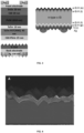
- the top of these textured Si substrates appears as pyramids, typically one to a few micrometers in length to the top and at the base (see Figure 1 ). For this reason, vacuum deposited perovskite front cells hold advantages over solution processed ones as vacuum processed perovskite can cover conformally all the pyramids.
- the present invention demonstrates the benefits of using an all-molecular semiconductor charge recombination junction (CRJ).
- CRJ all-molecular semiconductor charge recombination junction
- ITO simple thermal sublimation sources
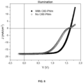
- a molecular CRJ was deposited, a much better yield and much better performances of working devices were surprisingly observed. There are indications that this may be related to a better adhesion of the front sub-cell to the Si cell.
- a double layer of molecular semiconductors was employed. Such junctions have been used in organic solar cells and also by us in perovskite-perovskite tandem cells (in which both sub-cells are based on perovskite absorbers), normally with different bandgaps.
- These CRJ comprise an electron transporting material (ETM) and a hole transporting material (HTM). To increase the conductivity these materials can be doped. The doping is achieved by partially reducing the electron transporting material (ETM) and by partially oxidizing the hole transporting material (HTM).
- the ratio of n-type dopant to ETM is in the range of 1:9 to 6:4, more preferable from 3:7 to 5:5.
- the ratio of p-type dopant to HTM is in the range of 0.5:10 to 3:7, more preferable from 1:10 to 2:8.
- a perovskite-silicon monolithic tandem cell comprises a Si-back sub-cell comprising a n-doped hydrogenated amorphous silicon a-Si:H (n) layer as the top layer, a metal halide perovskite front sub-cell and a charge recombination junction (CRJ) that joins these two sub-cells, the Si-back sub-cell and the perovskite front sub-cell.
- Si-back sub-cell comprising a n-doped hydrogenated amorphous silicon a-Si:H (n) layer as the top layer
- n n-doped hydrogenated amorphous silicon a-Si:H (n) layer
- n n-doped hydrogenated amorphous silicon a-Si:H (n) layer
- n n-doped hydrogenated amorphous silicon a-Si:H (n) layer
- metal halide perovskite front sub-cell
- the charge recombination junction further comprises a doped n-type molecular semiconductor layer comprising a partially reduced electron transporting material (ETM), as the bottom layer of the charge recombination junction CRJ, and a doped p-type molecular semiconductor a partially oxidized hole transporting material (HTM).
- ETM electron transporting material
- HTM partially oxidized hole transporting material
- the doped n-type molecular semiconductor layer is in contact with the n-doped hydrogenated amorphous silicon a-Si:H (n) layer of the Si-back sub-cell.
- This molecular CRJ is deposited on the Si-heterojunction cell containing as final top layer an n-doped hydrogenated amorphous silicon (a-Si:H (n)) layer.
- a-Si:H (n) n-doped hydrogenated amorphous silicon
- the top layer of the Si cell is a n-type layer the logical thing to do would be to deposit a p-type molecular layer to form an n-p junction (similar to a p-n junction, just grown inverted). However, this does not lead to good solar cells, probably because of the very low conductivity of the a-Si:H layer.
- the molecular CRJ of the invention comprises an electron transporting material (ETM) with the following requirements: it has a LUMO between -3.7 and -4.3 eV below vacuum (as determined by UPS, more preferably between -3.9 and -4.1 eV below vacuum) and a HOMO level below -5.6 eV below vacuum level.
- ETM electron transporting material
- Fullerenes are one class of molecules that fulfill these requirements. Examples are C 60 , C 70 and derivates such as PCBM ([6,6]-phenyl-C 61 -butyric acid methyl ester).
- an aromatic compound whose first reduction potential is in the range of about ⁇ 1.0 V, preferably ⁇ 0.5 V, compared to the reduction potential of C 60 when measured under the same conditions by cyclic voltammetry against Fc/Fc+ in acetonitrile can be selected as electron transporting material (ETM).
- ETM electron transporting material
- Examples of alternative aromatic electron transporting molecules are perylene's, fullerenones, and their derivatives.
- the electron transporting material (ETM) can be doped with either; a molecular dopant comprising an organic compound having a molecular weight of about 300 to about 1500 g/mol; or a metal dopant selected from the group consisting of a metal halide having a molecular weight of about 25 to about 500 g/mol, or a metal complex having a molecular weight of about 150 to about 1500 g/mol, or a zero-valent metal selected from the group consisting of alkali metal, alkaline earth metal, and rare earth metals. Additionally, the electron transporting material (ETM) can be doped.
- n-dopants can be elemental metals, inorganic salts, organic salts, organic hydride molecules and molecular dopants.
- elemental metals include Li, Ca, Na, K and Cs.
- organic salts include pyronin B chloride, crystal violet and pyronine B.
- molecular dopants examples include cobaltocene, decamethylcobaltocene, N1,N4-bis(tri-p-tolylphosphoranylidene) benzene-1,4-diamine (Phlm), tetrakis(hexahydropyrimidinopyrimidine)ditungsten(II) (W 2 (hpp) 4 ) and organic hydride compounds such as leuco crystal violet and derivates of 2,3-dihydro-1H-benzimidazoles (DMBI-H).
- DMBI-H, PhIM and W 2 (hpp) 4 can be used as n-dopant.
- N1,N4-bis(tri-p-tolylphosphoranylidene) benzene-1,4-diamine (Phlm) is used as p-dopant.
Landscapes
- Chemical & Material Sciences (AREA)
- Physics & Mathematics (AREA)
- Electromagnetism (AREA)
- Engineering & Computer Science (AREA)
- Materials Engineering (AREA)
- Inorganic Chemistry (AREA)
- Photovoltaic Devices (AREA)
Priority Applications (1)
| Application Number | Priority Date | Filing Date | Title |
|---|---|---|---|
| EP23307317.0A EP4577013A1 (de) | 2023-12-21 | 2023-12-21 | Monolithische perowskit-silicium tandemzellen mit molekularem ladungsrekombinationsübergang |
Applications Claiming Priority (1)
| Application Number | Priority Date | Filing Date | Title |
|---|---|---|---|
| EP23307317.0A EP4577013A1 (de) | 2023-12-21 | 2023-12-21 | Monolithische perowskit-silicium tandemzellen mit molekularem ladungsrekombinationsübergang |
Publications (1)
| Publication Number | Publication Date |
|---|---|
| EP4577013A1 true EP4577013A1 (de) | 2025-06-25 |
Family
ID=89619386
Family Applications (1)
| Application Number | Title | Priority Date | Filing Date |
|---|---|---|---|
| EP23307317.0A Pending EP4577013A1 (de) | 2023-12-21 | 2023-12-21 | Monolithische perowskit-silicium tandemzellen mit molekularem ladungsrekombinationsübergang |
Country Status (1)
| Country | Link |
|---|---|
| EP (1) | EP4577013A1 (de) |
Cited By (1)
| Publication number | Priority date | Publication date | Assignee | Title |
|---|---|---|---|---|
| CN120417625A (zh) * | 2025-07-04 | 2025-08-01 | 苏州晨晖智能设备有限公司 | 一种轻掺杂氢化非晶硅/钙钛矿异质结光伏电池、光伏组件及其制备方法 |
Citations (1)
| Publication number | Priority date | Publication date | Assignee | Title |
|---|---|---|---|---|
| WO2022096802A1 (fr) | 2020-11-05 | 2022-05-12 | Commissariat A L'energie Atomique Et Aux Energies Alternatives | Dispositif photovoltaïque tandem combinant une sous-cellule a base de silicium et une sous-cellule a base de perovskite comportant une couche composite perovskite/materiau de type p ou n |
-
2023
- 2023-12-21 EP EP23307317.0A patent/EP4577013A1/de active Pending
Patent Citations (1)
| Publication number | Priority date | Publication date | Assignee | Title |
|---|---|---|---|---|
| WO2022096802A1 (fr) | 2020-11-05 | 2022-05-12 | Commissariat A L'energie Atomique Et Aux Energies Alternatives | Dispositif photovoltaïque tandem combinant une sous-cellule a base de silicium et une sous-cellule a base de perovskite comportant une couche composite perovskite/materiau de type p ou n |
Non-Patent Citations (10)
| Title |
|---|
| "Hole-Transport Materials for Perovskite Solar Cells", ANGEW. CHEM. I NT. ED., vol. 55, 2016, pages 14522 - 14545 |
| ANITA W. Y. HO-BAILLIE: "Recent progress and future prospects of perovskite tandem solar cells", vol. 8, no. 4, 15 October 2021 (2021-10-15), United States, XP093167820, ISSN: 1931-9401, Retrieved from the Internet <URL:https://pubs.aip.org/aip/apr/article-pdf/doi/10.1063/5.0061483/19739398/041307_1_online.pdf> DOI: 10.1063/5.0061483 * |
| AYDIN, E. ET AL.: "Enhanced optoelectronic coupling for perovskite-silicon tandem solar cells", NATURE, 2023 |
| FORGÁCS DÁVID ET AL: "Efficient Monolithic Perovskite/Perovskite Tandem Solar Cells", vol. 7, no. 8, 14 December 2016 (2016-12-14), DE, pages 1602121, XP093080391, ISSN: 1614-6832, Retrieved from the Internet <URL:https://api.wiley.com/onlinelibrary/tdm/v1/articles/10.1002%2Faenm.201602121> DOI: 10.1002/aenm.201602121 * |
| FORGACS ET AL.: "Efficient Monolithic Perovskite/Perovskite Tandem Solar Cells", ADV. ENERGY MATER., vol. 7, 2017, pages 1602121, XP093080391, DOI: 10.1002/aenm.201602121 |
| LUSSEM ET AL.: "Doped Organic Transistors typical examples of n- and p-type dopants are described", CHEM. REV., vol. 116, 2016, pages 13714 - 13751 |
| MOMBLONA ET AL.: "Efficient vacuum deposited p-i-n and n-i-p perovskite solar cells employing doped charge transport layers", ENERGY ENVIRON. SCI., vol. 9, 2016, pages 3456 |
| PAUL M. BORSENBERGERDAVID S. WEISS: "Organic Photoreceptors for Imaging Systems", 1998, MARCEL DEKKER, INC |
| ZHENGJIE ZHU: "Perovskite tandem solar cells with improved efficiency and stability", JOURNAL OF ENERGY CHEMISTRY, vol. 58, 26 September 2020 (2020-09-26), AMSTERDAM, NL, pages 219 - 232, XP093167800, ISSN: 2095-4956, DOI: 10.1016/j.jechem.2020.09.022 * |
| ZHIHAO ZHANG ET AL: "Perovskite-Based Tandem Solar Cells: Get the Most Out of the Sun", ADVANCED FUNCTIONAL MATERIALS, WILEY - V C H VERLAG GMBH & CO. KGAA, DE, vol. 30, no. 38, 16 July 2020 (2020-07-16), pages n/a, XP072412305, ISSN: 1616-301X, DOI: 10.1002/ADFM.202001904 * |
Cited By (2)
| Publication number | Priority date | Publication date | Assignee | Title |
|---|---|---|---|---|
| CN120417625A (zh) * | 2025-07-04 | 2025-08-01 | 苏州晨晖智能设备有限公司 | 一种轻掺杂氢化非晶硅/钙钛矿异质结光伏电池、光伏组件及其制备方法 |
| CN120417625B (zh) * | 2025-07-04 | 2025-10-10 | 苏州晨晖智能设备有限公司 | 一种轻掺杂氢化非晶硅/钙钛矿异质结光伏电池、光伏组件及其制备方法 |
Similar Documents
| Publication | Publication Date | Title |
|---|---|---|
| Fu et al. | Monolithic perovskite‐silicon tandem solar cells: from the lab to fab? | |
| Ying et al. | Towards the 10‐year milestone of monolithic perovskite/silicon tandem solar cells | |
| Bush et al. | Minimizing current and voltage losses to reach 25% efficient monolithic two-terminal perovskite–silicon tandem solar cells | |
| Powalla et al. | Thin‐film solar cells exceeding 22% solar cell efficiency: An overview on CdTe-, Cu (In, Ga) Se2-, and perovskite-based materials | |
| Song et al. | Wide-bandgap, low-bandgap, and tandem perovskite solar cells | |
| US20220367739A1 (en) | Solar cell comprising a metal-oxide buffer layer and method of fabrication | |
| Sahli et al. | Improved optics in monolithic perovskite/silicon tandem solar cells with a nanocrystalline silicon recombination junction | |
| Albrecht et al. | Monolithic perovskite/silicon-heterojunction tandem solar cells processed at low temperature | |
| JP7032933B2 (ja) | ペロブスカイト材料を堆積させる方法 | |
| US10535791B2 (en) | 2-terminal metal halide semiconductor/C-silicon multijunction solar cell with tunnel junction | |
| KR102630952B1 (ko) | 페로브스카이트 재료의 침착 방법 | |
| EP3185323A1 (de) | Dotierte perovskite und deren verwendung als aktive und/oder ladungstransportschichten in optoelektronischen vorrichtungen | |
| US11489014B2 (en) | Monolithic solar cell | |
| Avila et al. | Influence of doped charge transport layers on efficient perovskite solar cells | |
| US20250185448A1 (en) | High-efficiency perovskite-based device with metal fluoride interlayer and method | |
| CN112136225A (zh) | 太阳能电池 | |
| Menon et al. | Hole Selectivity of n‐Type Molybdenum Oxide Carrier Selective Layer for Commercial and Emerging Thin‐Film Photovoltaics: A Critical Analysis of Interface Energetics and Ensuant Device Physics | |
| Hu et al. | Enhanced efficiency of the Sb2Se3 thin-film solar cell by the anode passivation using an organic small molecular of TCTA | |
| CN116548083A (zh) | 多层接合型光电转换元件及其制造方法 | |
| US20230345743A1 (en) | Multilayer junction photoelectric conversion element and method for manufacturing the same | |
| Parui et al. | Numerical and experimental insight on lead free MASnI3 based perovskite solar cell | |
| US12100562B2 (en) | Solar cell with alumina coated porous silicon layer | |
| WO2025018250A1 (ja) | タンデム型太陽電池、タンデム型太陽電池の製造方法 | |
| Paul et al. | Thermal Degradation Mechanisms and Stability Enhancement Strategies in Perovskite Solar Cells: A Review | |
| Jošt et al. | Highly efficient monolithic perovskite/CIGSe tandem solar cells on rough bottom cell surfaces |
Legal Events
| Date | Code | Title | Description |
|---|---|---|---|
| PUAI | Public reference made under article 153(3) epc to a published international application that has entered the european phase |
Free format text: ORIGINAL CODE: 0009012 |
|
| STAA | Information on the status of an ep patent application or granted ep patent |
Free format text: STATUS: THE APPLICATION HAS BEEN PUBLISHED |
|
| AK | Designated contracting states |
Kind code of ref document: A1 Designated state(s): AL AT BE BG CH CY CZ DE DK EE ES FI FR GB GR HR HU IE IS IT LI LT LU LV MC ME MK MT NL NO PL PT RO RS SE SI SK SM TR |
|
| STAA | Information on the status of an ep patent application or granted ep patent |
Free format text: STATUS: REQUEST FOR EXAMINATION WAS MADE |
|
| 17P | Request for examination filed |
Effective date: 20250903 |