EP4577006A1 - Optoelektronische vorrichtung und verfahren zu ihrer herstellung - Google Patents
Optoelektronische vorrichtung und verfahren zu ihrer herstellung Download PDFInfo
- Publication number
- EP4577006A1 EP4577006A1 EP24219549.3A EP24219549A EP4577006A1 EP 4577006 A1 EP4577006 A1 EP 4577006A1 EP 24219549 A EP24219549 A EP 24219549A EP 4577006 A1 EP4577006 A1 EP 4577006A1
- Authority
- EP
- European Patent Office
- Prior art keywords
- light
- optoelectronic device
- pores
- stack
- porous alumina
- Prior art date
- Legal status (The legal status is an assumption and is not a legal conclusion. Google has not performed a legal analysis and makes no representation as to the accuracy of the status listed.)
- Granted
Links
Images





Classifications
-
- H—ELECTRICITY
- H10—SEMICONDUCTOR DEVICES; ELECTRIC SOLID-STATE DEVICES NOT OTHERWISE PROVIDED FOR
- H10H—INORGANIC LIGHT-EMITTING SEMICONDUCTOR DEVICES HAVING POTENTIAL BARRIERS
- H10H29/00—Integrated devices, or assemblies of multiple devices, comprising at least one light-emitting semiconductor element covered by group H10H20/00
- H10H29/80—Constructional details
- H10H29/85—Packages
- H10H29/855—Optical field-shaping means, e.g. lenses
-
- H—ELECTRICITY
- H10—SEMICONDUCTOR DEVICES; ELECTRIC SOLID-STATE DEVICES NOT OTHERWISE PROVIDED FOR
- H10H—INORGANIC LIGHT-EMITTING SEMICONDUCTOR DEVICES HAVING POTENTIAL BARRIERS
- H10H29/00—Integrated devices, or assemblies of multiple devices, comprising at least one light-emitting semiconductor element covered by group H10H20/00
- H10H29/01—Manufacture or treatment
- H10H29/036—Manufacture or treatment of packages
- H10H29/0363—Manufacture or treatment of packages of optical field-shaping means
-
- H—ELECTRICITY
- H10—SEMICONDUCTOR DEVICES; ELECTRIC SOLID-STATE DEVICES NOT OTHERWISE PROVIDED FOR
- H10H—INORGANIC LIGHT-EMITTING SEMICONDUCTOR DEVICES HAVING POTENTIAL BARRIERS
- H10H29/00—Integrated devices, or assemblies of multiple devices, comprising at least one light-emitting semiconductor element covered by group H10H20/00
- H10H29/20—Assemblies of multiple devices comprising at least one light-emitting semiconductor device covered by group H10H20/00
- H10H29/24—Assemblies of multiple devices comprising at least one light-emitting semiconductor device covered by group H10H20/00 comprising multiple light-emitting semiconductor devices
-
- H—ELECTRICITY
- H10—SEMICONDUCTOR DEVICES; ELECTRIC SOLID-STATE DEVICES NOT OTHERWISE PROVIDED FOR
- H10H—INORGANIC LIGHT-EMITTING SEMICONDUCTOR DEVICES HAVING POTENTIAL BARRIERS
- H10H29/00—Integrated devices, or assemblies of multiple devices, comprising at least one light-emitting semiconductor element covered by group H10H20/00
- H10H29/80—Constructional details
- H10H29/85—Packages
- H10H29/851—Wavelength conversion means
- H10H29/8516—Wavelength conversion means having a non-uniform spatial arrangement or non-uniform concentration, e.g. patterned wavelength conversion layer, wavelength conversion layer with a concentration gradient
-
- H—ELECTRICITY
- H10—SEMICONDUCTOR DEVICES; ELECTRIC SOLID-STATE DEVICES NOT OTHERWISE PROVIDED FOR
- H10H—INORGANIC LIGHT-EMITTING SEMICONDUCTOR DEVICES HAVING POTENTIAL BARRIERS
- H10H29/00—Integrated devices, or assemblies of multiple devices, comprising at least one light-emitting semiconductor element covered by group H10H20/00
- H10H29/80—Constructional details
- H10H29/85—Packages
- H10H29/855—Optical field-shaping means, e.g. lenses
- H10H29/856—Reflecting means
-
- H—ELECTRICITY
- H10—SEMICONDUCTOR DEVICES; ELECTRIC SOLID-STATE DEVICES NOT OTHERWISE PROVIDED FOR
- H10W—GENERIC PACKAGES, INTERCONNECTIONS, CONNECTORS OR OTHER CONSTRUCTIONAL DETAILS OF DEVICES COVERED BY CLASS H10
- H10W90/00—Package configurations
-
- H—ELECTRICITY
- H10—SEMICONDUCTOR DEVICES; ELECTRIC SOLID-STATE DEVICES NOT OTHERWISE PROVIDED FOR
- H10H—INORGANIC LIGHT-EMITTING SEMICONDUCTOR DEVICES HAVING POTENTIAL BARRIERS
- H10H29/00—Integrated devices, or assemblies of multiple devices, comprising at least one light-emitting semiconductor element covered by group H10H20/00
- H10H29/01—Manufacture or treatment
- H10H29/036—Manufacture or treatment of packages
- H10H29/0361—Manufacture or treatment of packages of wavelength conversion means
-
- H—ELECTRICITY
- H10—SEMICONDUCTOR DEVICES; ELECTRIC SOLID-STATE DEVICES NOT OTHERWISE PROVIDED FOR
- H10H—INORGANIC LIGHT-EMITTING SEMICONDUCTOR DEVICES HAVING POTENTIAL BARRIERS
- H10H29/00—Integrated devices, or assemblies of multiple devices, comprising at least one light-emitting semiconductor element covered by group H10H20/00
- H10H29/80—Constructional details
- H10H29/85—Packages
- H10H29/851—Wavelength conversion means
- H10H29/8514—Wavelength conversion means characterised by their shape, e.g. plate or foil
-
- H—ELECTRICITY
- H10—SEMICONDUCTOR DEVICES; ELECTRIC SOLID-STATE DEVICES NOT OTHERWISE PROVIDED FOR
- H10H—INORGANIC LIGHT-EMITTING SEMICONDUCTOR DEVICES HAVING POTENTIAL BARRIERS
- H10H29/00—Integrated devices, or assemblies of multiple devices, comprising at least one light-emitting semiconductor element covered by group H10H20/00
- H10H29/80—Constructional details
- H10H29/882—Scattering means
Definitions
- the present invention relates to an optoelectronic device, in particular intended to equip a display screen or an image projection system.
- the present invention also relates to a method of manufacturing such an optoelectronic device.
- optoelectronic devices comprising a matrix of light-emitting diodes having an emitting surface coated at least in part with light color converters.
- Such optoelectronic devices can form display screens or image projection systems comprising a matrix of light pixels of different colors.
- the light-emitting diodes may be formed from a semiconductor material comprising elements from column III and column V of the periodic table, such as a III-V compound, including gallium nitride (GaN), indium gallium nitride (InGaN), or aluminum gallium nitride (AIGaN). They are arranged to form a matrix of light-emitting diodes having an emitting surface through which the light radiation emitted by the light-emitting diodes is transmitted.
- a III-V compound including gallium nitride (GaN), indium gallium nitride (InGaN), or aluminum gallium nitride (AIGaN).
- the optoelectronic device may thus comprise a matrix of luminous pixels, each luminous pixel comprising one or more light-emitting diodes.
- the light-emitting diodes may be adapted to emit blue light
- certain luminous pixels may be associated with light color converters, such as photoluminescent pads, adapted to absorb the blue light emitted by the light-emitting diodes, and to emit, in response, green or red light.
- the photoluminescent pads are usually formed from a binder matrix, called below resin, comprising particles of a photoluminescent material such as yttrium aluminum garnet (YAG) activated by the cerium ion YAG:Ce.
- YAG yttrium aluminum garnet
- the emission of light-emitting diodes, and therefore of pixels, is more or less angularly directive and optical crosstalk phenomena can be generated between pixels or between light-emitting diodes.
- the use of light color converters, such as the photoluminescent pads introduced above, can accentuate these optical crosstalk phenomena.
- the manufacturing method comprises the removal, for example by etching, of the porous alumina at the level of at least one, for example some, of said spaces, and the filling of at least one of the spaces thus hollowed out with a light color conversion material.
- the anodizing step comprises anodizing a portion of the aluminum-based layer that is located in line with at least one electrically conductive pad and depositing a reflective material in the pores of the porous alumina located in line with said at least one electrically conductive pad.
- a layer, wall, pad or element based on a material A means a layer, wall, pad or element comprising this material A and possibly other materials, respectively.
- a parameter that is "substantially equal to/greater than/less than” a given value means that this parameter is equal to/greater than/less than the given value, within plus or minus 20% or even 10% of this value.
- a parameter that is "substantially between” two given values means that this parameter is at least equal to the smallest given value, within plus or minus 20% or even 10% of this value, and at most equal to the largest given value, within plus or minus 20% or even 10% of this value.
- the terms “on”, “ surmounts”, “overhangs”, “covers”, “underlies” and their equivalents do not necessarily mean “in contact with”.
- the transfer, application or deposition of a first layer on a second layer does not necessarily mean that the two layers are in direct contact with each other, but means that the first layer at least partially covers the second layer by being either directly in contact with it or by being separated from it by at least one other layer or at least one other element.
- An element is said to be “microscopic" when its dimensions are equal to or less than a few micrometers.
- a microLED has dimensions equal to or less than a few micrometers.
- substrate, film or layer thicknesses are generally measured in directions perpendicular to the main plane of extension of the substrate, film or layer.
- the first aspect of the invention relates to an optoelectronic device 1.
- FIG. 9 illustrates an embodiment of the stack 11. It should be noted here that the illustration provided by the Figure 9 is structurally simplified. However, it is deemed sufficient to illustrate how the stack 11 is arranged relative to the other elements of each of the embodiments of the optoelectronic device 1. The person in the trade is deemed to know, by his general knowledge, at least one, or even several, of the complex structures that stack 11 can take.
- the first-type semiconductor layer 111a is a P-type semiconductor
- the second-type semiconductor layer 111c is an N-type semiconductor
- the light-emitting layer 112 is preferably a multiple quantum well or MQW layer, but this description is not limited to this example.
- the first type semiconductor layer 111a may be an N-type semiconductor
- the second type semiconductor layer 111c may be a P-type semiconductor.
- the matrix of emissive structures 1112 comprises at least the plurality of light-emitting diodes 111 and the plurality of electrically conductive pads 112. This matrix 1112 preferably forms a level of each of the embodiments of the optoelectronic device 1 according to the first aspect of the invention.
- the material forming the electrode layer 116 may be a transparent conductive material (TCM) which is a solid that does not absorb visible light (gap greater than 3 eV) and which has good electrical conductivity, indium-tin oxide (or ITO, acronym for Indium Tin Oxide), zinc oxide doped with aluminum or gallium, graphene, aluminum (preferably with a thickness substantially equal to 10 nm), zinc oxide doped with aluminum (AZO), or a combination of these materials.
- TCM transparent conductive material
- ITO Indium Tin Oxide
- the thickness of the electrode layer 116 may be between 0.03 ⁇ m and 1 ⁇ m. It should be noted that the presence of an electrode layer 116 in the stack 11 is optional, in particular to the extent that a lateral electrical contact 1171 may be provided to which we will return below.
- the electrical insulation provided by the dielectric wall 117 may only be partial, in particular since the optoelectronic device 1 does not include the aforementioned electrode layer 116. It is indeed at least preferable that, in this case, a lateral electrical contact 1171 (Cf. for example Figure 15 ) remains between one, or even each, electrically conductive pad 112 of the plurality and the second type semiconductor layer 111c of at least one, preferably each, of the adjacent light-emitting diodes 111.
- At least one, preferably each, emissive structure further comprises dielectric walls 117 including first dielectric walls 117a extending between at least one, preferably each, conductive pad 112 and the carrier substrate 113 and second dielectric walls 117b, called lateral walls, extending over at least a portion of the lateral sides of each conductive pad 112, the first and second dielectric walls 117a and 117b being preferably joined together, so that each conductive pad is electrically insulated over a portion of its periphery.
- the light confinement layer 12 extends over the stack 11. It comprises reflective walls 121.
- the latter are preferably located in line with the electrically conductive pads 112, and not in line with the light-emitting diodes 111, so as not to oppose the passage of the light emitted by the light-emitting diodes 111, and on the contrary so as to reflect the light emitted by the light-emitting diodes 111 and thus reduce optical crosstalk phenomena.
- At least one, potentially each, reflective wall 121 may be based on, or even made of, aluminum. Alternatively, it could be based on, or even made of, any material reflecting, in particular, the wavelengths emitted by the light-emitting diodes 111; it could, for example, be made of copper.
- one of the advantages of the present invention is to reduce the number of technological steps necessary for the manufacture of an optoelectronic device relative to existing methods; however, as we will see below, one of the advantageous characteristics of certain embodiments of the invention consists of the presence of porous alumina 122 in the confinement layer 12, this alumina being generated on the stack 11 by local anodization of a prior deposit of aluminum on the stack 11, said deposit also being able to make it possible to form the reflective walls 121 outside the anodized zones of the confinement layer 12. It is envisaged that at least some of the reflective walls 121 are not entirely made of aluminum.
- At least one, potentially each, reflective wall 121 may be made of aluminum.
- at least one, potentially each, reflective wall 121 may be based on porous alumina 1211 and a reflective or absorbent material 1212 located in the pores of the porous alumina 1211; this embodiment makes it possible to take advantage of the highly anisotropic nature of the anodization of aluminum in nanoporous alumina to obtain even more reflective and/or more absorbent walls 121, depending on the nature of the material filling the pores.
- each space 10 can be located in line with a pixel comprising, where appropriate, several light-emitting diodes 111 or a sub-pixel comprising, for example, a single light-emitting diode 111.
- the reflective walls 121 defining said space 10 extend in line with at least some, preferably each, of the electrically conductive pads 112 adjacent to said at least one light-emitting diode 111 in line with which the space 10 is located.
- porous alumina 122 is formed.
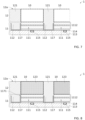
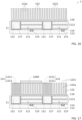
- the optoelectronic device 1 according to some of its different embodiments which are illustrated in the figures 1, 2 , 5, 6 , 17 And 18 is such that the light confinement layer 12 actually comprises porous alumina 122 in at least some of said spaces 10, the porous alumina 122 having, in at least one space, preferably at least two spaces, or even in each space, among said at least some of said spaces, at least two pores 1221 open on a first face 12a of the confinement layer 12 which is located opposite the stack 11.
- the embodiments which are illustrated on the figures 1, 2 , 5, 6 , 17 And 18 constitute all or part of final products, as opposed to intermediate products.
- Embodiments of the first aspect of the invention which are illustrated in the figures 3, 4 , 7 and 8 may also be considered as final products and may not include porous alumina 122 in line with certain of said spaces 10.
- These embodiments are preferably manufactured from optoelectronic devices according to the first aspect of the invention such as those illustrated in the figures 1 , 3 , 7 , And 17 , as intermediate products, the porous alumina 122 of these intermediate products having the advantage of being easy to etch to remove it in whole or in part, locally or everywhere.
- the pores 1221 of the porous alumina 122 located at the right of the spaces 10, whether they are those of the final products or of the aforementioned intermediate products, preferably have transverse dimensions of between 1 and 500 nm and preferably between 50 and 400 nm.
- the pores 1221 of the porous alumina 122 preferably have a periodicity of between 200 and 700 nm.
- the size of the pores is preferably greater than the size of the color conversion particles that it is desired to slide inside, so as to be able to have at least one color conversion particle in each pore.
- the transverse dimension of the pores 1221 can therefore depend on the size of the particles of the light color conversion material that are intended to be introduced therein; the parameters of the anodization of the aluminum layer to form the porous alumina are preferably set accordingly.
- the porous alumina 122 located where appropriate in line with the electrically conductive pads 112 may have the same characteristics as those stated above to qualify the porous alumina 122 located in at least some of the spaces 10.
- the light color conversion material 123 is preferably grafted to the inner walls of pores 1221.
- the aforementioned solvent or resin may play an advantageous role in the formation of such grafts.
- the particles of the light color conversion material 123 and/or the inner walls of the pores 1221 may be functionalized, before, or even during, the deposition of the light color conversion material 123 in the pores 1221 of the porous alumina 122, so as to obtain a grafting of them to each other, for example by surface hydrogen bonds -OH, created where appropriate by treatment with alkaline chemistry or by treatment with dry plasma or by adsorption of a ligand.
- At least one, preferably each, pore 1221 open on the first face 12a of the confinement layer 12 which is located opposite the stack 11 preferably has a filling rate, in the light color conversion material, substantially equal to 30%. Achieving such filling can be made easy by the aforementioned grafting.
- the optoelectronic device 1 The optoelectronic device 1
- the light-emitting diodes 111 can be configured to emit light of a first determined wavelength, for example the color blue, in a direction substantially perpendicular to the first face 12a of the confinement layer 12.
- the light color conversion material 123 may be capable of converting the light emitted at the first wavelength into light having a second wavelength different from the first, for example the first wavelength being in the blue range and the second wavelength being in one or other of green and red.
- the green light thus converted is of a wavelength substantially in the range from 510 nm to 570 nm.
- the red light thus converted is of a wavelength substantially in the range from 600 nm to 720 nm.
- the pores 1221 of the porous alumina 122 form channels 122a opening onto the first face 12a of the confinement layer 12.
- the channels 122a preferably extend mainly in a direction perpendicular to the first surface 12a of the confinement layer 12; they can more particularly extend over a distance Lp, taken in projection in a direction perpendicular to the first face 12a, strictly greater than half of a thickness E12 of the confinement layer 12.
- the pores 1221 can extend substantially up to the stack 11, preferably without reaching it (except in the presence of the aluminum pads above the conductive pads, these aluminum pads preventing delamination of the structure), so as to limit any risk of delamination, to present a maximized internal wall surface, and thus maximize the aforementioned grafting, and consequently the filling of the pores by the light color conversion material 123.
- at least one, preferably each, pore 1221 can have a form factor defined by transverse dimensions substantially between 40 nm and 800 nm, and/or a longitudinal dimension substantially between 500 nm and 10 ⁇ m, preferably substantially between 1 ⁇ m and 5 ⁇ m.
- this deposition is extended to form the aluminum layer 2000 of thickness E12 on the stack 11, then the localized anodization, thanks to masks 2100, of the zones of the aluminum layer 2000 which are located at the right of the light-emitting diodes 111, to arrive at an optoelectronic device as illustrated on the Figure 15 , from which it is sufficient to remove the masks 2100 to obtain the optoelectronic device as illustrated in the Figure 5 .
- the pores 1221 thus formed can then be filled with a light color conversion material 123 as detailed above to obtain the optoelectronic device as illustrated in the Figure 6 .
Landscapes
- Led Devices (AREA)
- Led Device Packages (AREA)
Applications Claiming Priority (1)
| Application Number | Priority Date | Filing Date | Title |
|---|---|---|---|
| FR2314363A FR3156994B1 (fr) | 2023-12-18 | 2023-12-18 | Dispositif optoélectronique et procédé de fabrication associé |
Publications (2)
| Publication Number | Publication Date |
|---|---|
| EP4577006A1 true EP4577006A1 (de) | 2025-06-25 |
| EP4577006B1 EP4577006B1 (de) | 2026-04-29 |
Family
ID=90904688
Family Applications (1)
| Application Number | Title | Priority Date | Filing Date |
|---|---|---|---|
| EP24219549.3A Active EP4577006B1 (de) | 2023-12-18 | 2024-12-12 | Optoelektronische vorrichtung und verfahren zu ihrer herstellung |
Country Status (4)
| Country | Link |
|---|---|
| US (1) | US20250204134A1 (de) |
| EP (1) | EP4577006B1 (de) |
| CN (1) | CN120187182A (de) |
| FR (1) | FR3156994B1 (de) |
Citations (8)
| Publication number | Priority date | Publication date | Assignee | Title |
|---|---|---|---|---|
| EP2708492B1 (de) | 2012-07-13 | 2017-11-29 | CSEM Centre Suisse d'Electronique et de Microtechnique SA - Recherche et Développement | Mesoporöse Schicht mit J-Aggregaten und Herstellungsverfahren |
| FR3061358A1 (fr) | 2016-12-27 | 2018-06-29 | Aledia | Procede de fabrication d’un dispositif optoelectronique comportant des plots photoluminescents de photoresine |
| FR3083370A1 (fr) | 2018-06-28 | 2020-01-03 | Aledia | Dispositif émetteur, écran d'affichage associé et procédé de fabrication d'un dispositif émetteur |
| FR3087580A1 (fr) | 2018-10-23 | 2020-04-24 | Aledia | Procede de realisation d’un dispositif optoelectronique comprenant des diodes electroluminescentes homogenes en dimensions |
| FR3101130A1 (fr) | 2019-09-25 | 2021-03-26 | Renault S.A.S | Véhicule comprenant un projecteur réglable |
| US20230033031A1 (en) | 2021-07-29 | 2023-02-02 | PlayNitride Display Co., Ltd. | Micro light-emitting diode display device and manufacturing method thereof |
| US20230155075A1 (en) * | 2021-11-16 | 2023-05-18 | Nanosys, Inc. | Light emitting devices including a quantum dot color conversion material and method of making thereof |
| CN116469987A (zh) * | 2023-03-31 | 2023-07-21 | 华为技术有限公司 | 显示面板和电子设备 |
-
2023
- 2023-12-18 FR FR2314363A patent/FR3156994B1/fr active Active
-
2024
- 2024-12-12 EP EP24219549.3A patent/EP4577006B1/de active Active
- 2024-12-17 US US18/984,215 patent/US20250204134A1/en active Pending
- 2024-12-18 CN CN202411871084.6A patent/CN120187182A/zh active Pending
Patent Citations (8)
| Publication number | Priority date | Publication date | Assignee | Title |
|---|---|---|---|---|
| EP2708492B1 (de) | 2012-07-13 | 2017-11-29 | CSEM Centre Suisse d'Electronique et de Microtechnique SA - Recherche et Développement | Mesoporöse Schicht mit J-Aggregaten und Herstellungsverfahren |
| FR3061358A1 (fr) | 2016-12-27 | 2018-06-29 | Aledia | Procede de fabrication d’un dispositif optoelectronique comportant des plots photoluminescents de photoresine |
| FR3083370A1 (fr) | 2018-06-28 | 2020-01-03 | Aledia | Dispositif émetteur, écran d'affichage associé et procédé de fabrication d'un dispositif émetteur |
| FR3087580A1 (fr) | 2018-10-23 | 2020-04-24 | Aledia | Procede de realisation d’un dispositif optoelectronique comprenant des diodes electroluminescentes homogenes en dimensions |
| FR3101130A1 (fr) | 2019-09-25 | 2021-03-26 | Renault S.A.S | Véhicule comprenant un projecteur réglable |
| US20230033031A1 (en) | 2021-07-29 | 2023-02-02 | PlayNitride Display Co., Ltd. | Micro light-emitting diode display device and manufacturing method thereof |
| US20230155075A1 (en) * | 2021-11-16 | 2023-05-18 | Nanosys, Inc. | Light emitting devices including a quantum dot color conversion material and method of making thereof |
| CN116469987A (zh) * | 2023-03-31 | 2023-07-21 | 华为技术有限公司 | 显示面板和电子设备 |
Non-Patent Citations (1)
| Title |
|---|
| SIONTAS ET AL.: "Broadband visible-to-telecom wavelength germanium quantum dot photodetectors", APPLIED PHYSICS LETTERS, vol. 113, 2018, pages 251901, XP012232859, DOI: 10.1063/1.5052252 |
Also Published As
| Publication number | Publication date |
|---|---|
| US20250204134A1 (en) | 2025-06-19 |
| FR3156994A1 (fr) | 2025-06-20 |
| FR3156994B1 (fr) | 2026-06-26 |
| EP4577006B1 (de) | 2026-04-29 |
| CN120187182A (zh) | 2025-06-20 |
Similar Documents
| Publication | Publication Date | Title |
|---|---|---|
| EP3667728B1 (de) | Verfahren zur herstellung einer vorrichtung mit lichtemittierenden und/oder lichtempfangenden dioden und mit einem selbst ausgerichteten kollimationsgitter | |
| EP3185294B1 (de) | Optoelektronische vorrichtung zur lichtabgabe | |
| EP3563420B1 (de) | Verfahren zur herstellung einer optoelektronischen vorrichtung mit fotolumineszenten pads aus fotolack | |
| EP3127159B1 (de) | Halbleitendes pixel, matrix aus solchen pixeln, halbleitende struktur zur herstellung solcher pixel und deren herstellungsverfahren | |
| EP3699967B1 (de) | Leuchtdiode, pixel, der eine vielzahl von leuchtdioden umfasst, und entsprechende herstellungsverfahren | |
| WO2017068029A1 (fr) | Diode micro-electronique a surface active optimisee | |
| EP4615198A2 (de) | Verfahren zur herstellung einer optoelektronischen vorrichtung mit einer vielzahl von galliumnitriddioden | |
| EP3815143B1 (de) | Verfahren zur herstellung einer optoelektronischen vorrichtung mit selbstausgerichteten lichtbegrenzenden wänden | |
| EP3929634B1 (de) | Lichtemittierende vorrichtung, pixel mit einer vielzahl solcher vorrichtungen, pixelmatrix und entsprechende herstellungsverfahren | |
| FR3087580A1 (fr) | Procede de realisation d’un dispositif optoelectronique comprenant des diodes electroluminescentes homogenes en dimensions | |
| WO2024003085A1 (fr) | Dispositif optoélectronique et procédé de fabrication | |
| EP4577006B1 (de) | Optoelektronische vorrichtung und verfahren zu ihrer herstellung | |
| EP3871272A1 (de) | Optoelektronische vorrichtung, zugehöriger bildschirm und verfahren zur herstellung einer solchen optoelektronischen vorrichtung | |
| EP3871255B1 (de) | Optoelektronische vorrichtung mit leuchtdioden mit verbesserter lichtextraktion und ein verfahren zu seiner herstellung | |
| WO2017001760A1 (fr) | Dispositif electroluminescent a semiconducteur comportant une couche photoluminescente structuree | |
| FR3076080A1 (fr) | Pseudo-substrat pour dispositif optoelectronique et son procede de fabrication | |
| FR3103322A1 (fr) | Procédé de fabrication d’un ensemble d’émetteurs de lumière | |
| FR3082662A1 (fr) | Procédé de fabrication d’un dispositif optoélectronique à parois de confinement lumineux auto alignés | |
| EP4621847A1 (de) | Optoelektronische vorrichtung mit einer lichtemittierenden diode, die mit einem photodetektor überlagert ist | |
| FR3144412A1 (fr) | PROCEDE DE FABRICATION DE MICRO-LEDs | |
| EP4383338A1 (de) | Verfahren zur herstellung einer optoelektronischen vorrichtung mit einer led und einer photodiode | |
| WO2023247456A1 (fr) | Elément émetteur de lumière à générateur d'onde stationnaire et dispositif optoélectronique associé |
Legal Events
| Date | Code | Title | Description |
|---|---|---|---|
| PUAI | Public reference made under article 153(3) epc to a published international application that has entered the european phase |
Free format text: ORIGINAL CODE: 0009012 |
|
| STAA | Information on the status of an ep patent application or granted ep patent |
Free format text: STATUS: REQUEST FOR EXAMINATION WAS MADE |
|
| 17P | Request for examination filed |
Effective date: 20241212 |
|
| AK | Designated contracting states |
Kind code of ref document: A1 Designated state(s): AL AT BE BG CH CY CZ DE DK EE ES FI FR GB GR HR HU IE IS IT LI LT LU LV MC ME MK MT NL NO PL PT RO RS SE SI SK SM TR |
|
| GRAP | Despatch of communication of intention to grant a patent |
Free format text: ORIGINAL CODE: EPIDOSNIGR1 |
|
| STAA | Information on the status of an ep patent application or granted ep patent |
Free format text: STATUS: GRANT OF PATENT IS INTENDED |
|
| RIC1 | Information provided on ipc code assigned before grant |
Ipc: H10H 29/01 20250101AFI20251121BHEP Ipc: H10H 29/856 20250101ALI20251121BHEP Ipc: H10H 29/851 20250101ALN20251121BHEP Ipc: H10H 29/80 20250101ALN20251121BHEP |
|
| RIC1 | Information provided on ipc code assigned before grant |
Ipc: H10H 29/01 20250101AFI20251210BHEP Ipc: H10H 29/856 20250101ALI20251210BHEP Ipc: H10H 29/851 20250101ALN20251210BHEP Ipc: H10H 29/80 20250101ALN20251210BHEP |
|
| INTG | Intention to grant announced |
Effective date: 20251218 |
|
| RIN1 | Information on inventor provided before grant (corrected) |
Inventor name: PERNEL, CAROLE Inventor name: ALTAZIN, STEPHANE Inventor name: QUESNEL, ETIENNE |
|
| GRAS | Grant fee paid |
Free format text: ORIGINAL CODE: EPIDOSNIGR3 |
|
| GRAA | (expected) grant |
Free format text: ORIGINAL CODE: 0009210 |
|
| STAA | Information on the status of an ep patent application or granted ep patent |
Free format text: STATUS: THE PATENT HAS BEEN GRANTED |
|
| AK | Designated contracting states |
Kind code of ref document: B1 Designated state(s): AL AT BE BG CH CY CZ DE DK EE ES FI FR GB GR HR HU IE IS IT LI LT LU LV MC ME MK MT NL NO PL PT RO RS SE SI SK SM TR |
|
| REG | Reference to a national code |
Ref country code: CH Ref legal event code: F10 Free format text: ST27 STATUS EVENT CODE: U-0-0-F10-F00 (AS PROVIDED BY THE NATIONAL OFFICE) Effective date: 20260429 Ref country code: GB Ref legal event code: FG4D Free format text: NOT ENGLISH |
|
| REG | Reference to a national code |
Ref country code: IE Ref legal event code: FG4D Free format text: LANGUAGE OF EP DOCUMENT: FRENCH |
|
| REG | Reference to a national code |
Ref country code: DE Ref legal event code: R096 Ref document number: 602024004420 Country of ref document: DE |