EP4576984A1 - Ferroelektrische speicheranordnung und verfahren zu ihrer herstellung - Google Patents
Ferroelektrische speicheranordnung und verfahren zu ihrer herstellung Download PDFInfo
- Publication number
- EP4576984A1 EP4576984A1 EP24222243.8A EP24222243A EP4576984A1 EP 4576984 A1 EP4576984 A1 EP 4576984A1 EP 24222243 A EP24222243 A EP 24222243A EP 4576984 A1 EP4576984 A1 EP 4576984A1
- Authority
- EP
- European Patent Office
- Prior art keywords
- layer
- deposition
- ferroelectric material
- ferroelectric
- cavity
- Prior art date
- Legal status (The legal status is an assumption and is not a legal conclusion. Google has not performed a legal analysis and makes no representation as to the accuracy of the status listed.)
- Pending
Links
Images


Classifications
-
- H—ELECTRICITY
- H10—SEMICONDUCTOR DEVICES; ELECTRIC SOLID-STATE DEVICES NOT OTHERWISE PROVIDED FOR
- H10N—ELECTRIC SOLID-STATE DEVICES NOT OTHERWISE PROVIDED FOR
- H10N70/00—Solid-state devices having no potential barriers, and specially adapted for rectifying, amplifying, oscillating or switching
- H10N70/20—Multistable switching devices, e.g. memristors
-
- H—ELECTRICITY
- H10—SEMICONDUCTOR DEVICES; ELECTRIC SOLID-STATE DEVICES NOT OTHERWISE PROVIDED FOR
- H10N—ELECTRIC SOLID-STATE DEVICES NOT OTHERWISE PROVIDED FOR
- H10N70/00—Solid-state devices having no potential barriers, and specially adapted for rectifying, amplifying, oscillating or switching
- H10N70/011—Manufacture or treatment of multistable switching devices
- H10N70/061—Shaping switching materials
- H10N70/066—Shaping switching materials by filling of openings, e.g. damascene method
-
- H—ELECTRICITY
- H10—SEMICONDUCTOR DEVICES; ELECTRIC SOLID-STATE DEVICES NOT OTHERWISE PROVIDED FOR
- H10B—ELECTRONIC MEMORY DEVICES
- H10B63/00—Resistance change memory devices, e.g. resistive RAM [ReRAM] devices
-
- H—ELECTRICITY
- H10—SEMICONDUCTOR DEVICES; ELECTRIC SOLID-STATE DEVICES NOT OTHERWISE PROVIDED FOR
- H10D—INORGANIC ELECTRIC SEMICONDUCTOR DEVICES
- H10D1/00—Resistors, capacitors or inductors
- H10D1/60—Capacitors
- H10D1/68—Capacitors having no potential barriers
- H10D1/682—Capacitors having no potential barriers having dielectrics comprising perovskite structures
- H10D1/684—Capacitors having no potential barriers having dielectrics comprising perovskite structures the dielectrics comprising multiple layers, e.g. comprising buffer layers, seed layers or gradient layers
-
- H—ELECTRICITY
- H10—SEMICONDUCTOR DEVICES; ELECTRIC SOLID-STATE DEVICES NOT OTHERWISE PROVIDED FOR
- H10D—INORGANIC ELECTRIC SEMICONDUCTOR DEVICES
- H10D1/00—Resistors, capacitors or inductors
- H10D1/60—Capacitors
- H10D1/68—Capacitors having no potential barriers
- H10D1/692—Electrodes
- H10D1/711—Electrodes having non-planar surfaces, e.g. formed by texturisation
- H10D1/716—Electrodes having non-planar surfaces, e.g. formed by texturisation having vertical extensions
-
- H—ELECTRICITY
- H10—SEMICONDUCTOR DEVICES; ELECTRIC SOLID-STATE DEVICES NOT OTHERWISE PROVIDED FOR
- H10N—ELECTRIC SOLID-STATE DEVICES NOT OTHERWISE PROVIDED FOR
- H10N70/00—Solid-state devices having no potential barriers, and specially adapted for rectifying, amplifying, oscillating or switching
- H10N70/011—Manufacture or treatment of multistable switching devices
- H10N70/021—Formation of switching materials, e.g. deposition of layers
- H10N70/026—Formation of switching materials, e.g. deposition of layers by physical vapor deposition, e.g. sputtering
-
- H—ELECTRICITY
- H10—SEMICONDUCTOR DEVICES; ELECTRIC SOLID-STATE DEVICES NOT OTHERWISE PROVIDED FOR
- H10N—ELECTRIC SOLID-STATE DEVICES NOT OTHERWISE PROVIDED FOR
- H10N70/00—Solid-state devices having no potential barriers, and specially adapted for rectifying, amplifying, oscillating or switching
- H10N70/011—Manufacture or treatment of multistable switching devices
- H10N70/041—Modification of switching materials after formation, e.g. doping
- H10N70/043—Modification of switching materials after formation, e.g. doping by implantation
-
- H—ELECTRICITY
- H10—SEMICONDUCTOR DEVICES; ELECTRIC SOLID-STATE DEVICES NOT OTHERWISE PROVIDED FOR
- H10N—ELECTRIC SOLID-STATE DEVICES NOT OTHERWISE PROVIDED FOR
- H10N70/00—Solid-state devices having no potential barriers, and specially adapted for rectifying, amplifying, oscillating or switching
- H10N70/011—Manufacture or treatment of multistable switching devices
- H10N70/061—Shaping switching materials
-
- H—ELECTRICITY
- H10—SEMICONDUCTOR DEVICES; ELECTRIC SOLID-STATE DEVICES NOT OTHERWISE PROVIDED FOR
- H10N—ELECTRIC SOLID-STATE DEVICES NOT OTHERWISE PROVIDED FOR
- H10N70/00—Solid-state devices having no potential barriers, and specially adapted for rectifying, amplifying, oscillating or switching
- H10N70/20—Multistable switching devices, e.g. memristors
- H10N70/25—Multistable switching devices, e.g. memristors based on bulk electronic defects, e.g. trapping of electrons
-
- H—ELECTRICITY
- H10—SEMICONDUCTOR DEVICES; ELECTRIC SOLID-STATE DEVICES NOT OTHERWISE PROVIDED FOR
- H10N—ELECTRIC SOLID-STATE DEVICES NOT OTHERWISE PROVIDED FOR
- H10N70/00—Solid-state devices having no potential barriers, and specially adapted for rectifying, amplifying, oscillating or switching
- H10N70/801—Constructional details of multistable switching devices
- H10N70/821—Device geometry
-
- H—ELECTRICITY
- H10—SEMICONDUCTOR DEVICES; ELECTRIC SOLID-STATE DEVICES NOT OTHERWISE PROVIDED FOR
- H10N—ELECTRIC SOLID-STATE DEVICES NOT OTHERWISE PROVIDED FOR
- H10N70/00—Solid-state devices having no potential barriers, and specially adapted for rectifying, amplifying, oscillating or switching
- H10N70/801—Constructional details of multistable switching devices
- H10N70/821—Device geometry
- H10N70/826—Device geometry adapted for essentially vertical current flow, e.g. sandwich or pillar type devices
- H10N70/8265—Device geometry adapted for essentially vertical current flow, e.g. sandwich or pillar type devices on sidewalls of dielectric structures, e.g. mesa-shaped or cup-shaped devices
-
- H—ELECTRICITY
- H10—SEMICONDUCTOR DEVICES; ELECTRIC SOLID-STATE DEVICES NOT OTHERWISE PROVIDED FOR
- H10N—ELECTRIC SOLID-STATE DEVICES NOT OTHERWISE PROVIDED FOR
- H10N70/00—Solid-state devices having no potential barriers, and specially adapted for rectifying, amplifying, oscillating or switching
- H10N70/801—Constructional details of multistable switching devices
- H10N70/881—Switching materials
- H10N70/883—Oxides or nitrides
- H10N70/8833—Binary metal oxides, e.g. TaOx
-
- H—ELECTRICITY
- H10—SEMICONDUCTOR DEVICES; ELECTRIC SOLID-STATE DEVICES NOT OTHERWISE PROVIDED FOR
- H10N—ELECTRIC SOLID-STATE DEVICES NOT OTHERWISE PROVIDED FOR
- H10N70/00—Solid-state devices having no potential barriers, and specially adapted for rectifying, amplifying, oscillating or switching
- H10N70/801—Constructional details of multistable switching devices
- H10N70/881—Switching materials
- H10N70/883—Oxides or nitrides
- H10N70/8836—Complex metal oxides, e.g. perovskites, spinels
-
- H—ELECTRICITY
- H10—SEMICONDUCTOR DEVICES; ELECTRIC SOLID-STATE DEVICES NOT OTHERWISE PROVIDED FOR
- H10D—INORGANIC ELECTRIC SEMICONDUCTOR DEVICES
- H10D1/00—Resistors, capacitors or inductors
- H10D1/60—Capacitors
- H10D1/68—Capacitors having no potential barriers
- H10D1/692—Electrodes
- H10D1/694—Electrodes comprising noble metals or noble metal oxides
-
- H—ELECTRICITY
- H10—SEMICONDUCTOR DEVICES; ELECTRIC SOLID-STATE DEVICES NOT OTHERWISE PROVIDED FOR
- H10D—INORGANIC ELECTRIC SEMICONDUCTOR DEVICES
- H10D1/00—Resistors, capacitors or inductors
- H10D1/60—Capacitors
- H10D1/68—Capacitors having no potential barriers
- H10D1/692—Electrodes
- H10D1/696—Electrodes comprising multiple layers, e.g. comprising a barrier layer and a metal layer
Definitions
- the present invention relates generally to the field of microelectronics. It relates more particularly to the field of non-volatile memories.
- the invention relates to a ferroelectric storage device. It also relates to a method of manufacturing such a ferroelectric storage device.
- the reading operation involves the application of a reading voltage -Vr.
- the reading voltage -Vr is, for example, negative and lower in absolute value than a voltage Vc associated with the coercive field. This then makes it possible to perform a non-destructive reading by measuring a tunnel current.
- Multilevel data storage memory using deterministic polarization control. » by Lee, Daesu et al., in Advanced materials, vol. 24(3), 2012, 402-406, doi:10.1002/adma.201103679 describes a ferroelectric memory of the FeRAM type having several storage levels.
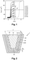
- the memory can be placed in several intermediate remanent polarization states Pr 1 , Pr 2 , Prs, Pr 4 , Pr 5 , Pr 6 , Pr 7 (Pr 0 corresponding to the low polarization state 0). It will therefore be possible to store the information at different levels.
- each intermediate polarization state Pr 1 , Pr 2 , Prs, Pr 4 , Pr 5 , Pr 6 , Pr 7 is associated with a corresponding current.
- an associated ferroelectric current is read. This current then makes it possible to identify the intermediate polarization state Pr 1 , Pr 2 , Pr 3 , Pr 4 , Pr 5 , Pr 6 , Pr 7 concerned and therefore to go back to the information initially stored in this intermediate polarization state Pr 1 , Pr 2 , Pr 3 , Pr 4 , Pr 5 , Pr 6 , Pr 7 of the ferroelectric memory.
- the present invention therefore aims to improve high-density ferroelectric storage devices by enabling unambiguous distinction of the different polarization states.
- the layer of ferroelectric material of the ferroelectric storage device has a non-uniform thickness.
- This variability of thicknesses results in a non-uniformity in the ferroelectric properties of the ferroelectric storage device.
- This non-uniformity of properties makes it possible in particular to increase the differences between the voltage ranges to be applied to store the information in the different intermediate polarization states.
- the different thicknesses then imply that, for a given (write) voltage, the electric field is greater in the thinner regions.
- a greater voltage must be applied to write information in an intermediate polarization state associated with a thin thickness.
- the differences in thickness therefore lead to differences in the voltages to be applied to encode the information in the different intermediate polarization states.
- the different thicknesses used are therefore associated with different intermediate polarization states in the ferroelectric storage device.
- the present invention aims to improve the manufacture of ferroelectric storage devices.
- the present invention relates to a high-density storage device in which several polarization states are used to store information.
- the present invention then aims to improve the definition of the polarization states in order to be able to clearly distinguish them in order to then be able to read the information stored and associated with each of the polarization states.
- FIG. 2 represents a ferroelectric storage device 1 (also referred to as device 1 hereinafter) according to the invention.
- the ferroelectric storage device 1 comprises a first layer 2, a second layer 7 and a layer of ferroelectric material 5 which is arranged between the first layer 2 and the second layer 7.
- the ferroelectric storage device 1 is in the form of a stack of layers.
- the first layer 2, the layer of ferroelectric material 5 and the second layer 7 form the different layers of this stack.
- the ferroelectric storage device 1 is formed in a cavity 50 (visible in the figures 5 to 10 and the figures 12 to 14 ).
- This support layer 10 is here formed from a dielectric material.
- the support layer 10 comprises silicon oxide SiO 2 .
- the support layer may comprise a plurality of sub-layers.
- the support layer may comprise another layer of dielectric material formed under the layer comprising silicon oxide SiO 2 .
- This other layer comprises for example silicon nitride SiN or silicon carbonitride SiCN.
- the cavity 50 comprises a bottom wall 52 and a side wall 55.
- the bottom wall 52 corresponds to the base of the “U” shape and the side wall 55 corresponds to the lateral branches of the “U” shape.
- the side wall 55 forms an angle of inclination ⁇ relative to an axis z, corresponding to a direction normal to the bottom wall 52.
- this angle of inclination ⁇ is non-zero.
- This angle of inclination ⁇ is for example less than 50 degrees.
- it is for example less than 35 degrees.
- this angle of inclination may be zero (the side wall is therefore vertical).
- the angle of inclination of the side wall 55 is substantially zero while on the figures 5 to 10 and the figures 12 to 14 , this inclination angle ⁇ is non-zero.
- the present invention finds a preferred application in the context of ferroelectric storage devices formed in such a support provided with a cavity having a bottom wall and a side wall.
- the stack forming the ferroelectric storage device 1 extends from the bottom wall 52 and the side wall 55. This stack then comprises several parts: one extending from the bottom wall 52 and another extending from the side wall 55. For the part formed on the bottom wall 52, the different layers of the stack extend parallel to each other. The same is true for the part extending from the side wall 55 (the different layers of the stack also extend parallel to each other on this side wall 55).
- the sidewall of the cavity may comprise a plurality of portions forming distinct angles relative to a direction normal to the bottom wall.
- the sidewall of the cavity could have a plurality of slope breaks.
- the first layer 2 is formed from an inert conductive material.
- This first layer 2 comprises, for example, a metallic material.
- the first layer comprises a single layer.
- the conductive material of this single layer comprises, for example, titanium nitride TiN.
- the conductive material may be tantalum nitride TaN or tungsten W.
- other conductive materials may be used (and in particular, metal nitride more generally).
- the first layer 2 is here in the form of a two-layer structure. It comprises here a first sub-layer 20 and a second sub-layer 22.
- the second sub-layer 22 is arranged on the first sub-layer 20.
- the first sub-layer 20 comprises a metallic conductive material.
- a metallic conductive material Preferably, it comprises titanium Ti or tantalum nitride TaN.
- the first sub-layer 20 has a thickness of between 3 and 20 nanometers (nm). Preferably, this thickness is between 5 and 10 nm.
- This first sub-layer 20 plays both the role of a protective layer and the role of a contact layer allowing the device 1 to be electrically connected to its electronic control and reading circuit.
- the second sub-layer 22 is arranged on the first sub-layer 20. It is in direct contact with the layer of ferroelectric material 5. In other words, the second sub-layer 22 extends between the first sub-layer 20 and the layer of ferroelectric material 5.
- the first sub-layer 20 is formed from a conductive material such as titanium Ti.
- the first sub-layer 20 is formed from a conductive titanium Ti material.
- the first sub-layer 70 is arranged on the layer of ferroelectric material 5. It is in direct contact with the layer of ferroelectric material 5. In other words, the first sub-layer 70 of the second layer 7 extends between the second sub-layer 72 and the layer of ferroelectric material 5.
- This first layer 2 is deposited in the cavity 50. More particularly, the first layer 2 is deposited along the bottom wall 52 and the side wall 55 of the cavity 50. The first layer 2 therefore lines and conforms to the shape of the cavity 50.
- the first layer 2 here comprises a first sub-layer 20 and a second sub-layer 22.
- Step E104 of depositing the first layer 2 therefore comprises two sub-steps here: a first sub-step E104a of depositing the first sub-layer 20 and a second sub-step E104b of depositing the second sub-layer 22.
- the first sub-layer 20 is therefore first deposited, in a conformal manner, in the cavity 50 (step E104a).
- the first sub-layer 20 is for example formed by an atomic layer deposition (or ALD) method or by chemical vapor deposition.
- the first sub-layer 20 may be formed by cathode sputtering in a vacuum deposition chamber.
- the first sub-layer 20 is formed from titanium nitride, it is a reactive cathode sputtering.
- the second sub-layer 22 of the first layer 2 is deposited, in a conformal manner, on the first sub-layer 20 (step E104b).
- the second sub-layer 22 is for example formed by cathode sputtering in a vacuum deposition chamber.
- the second sub-layer 22 of the first layer 2 is formed in the same deposition chamber as the first sub-layer 20 of the first layer 2.
- the second sub-layer 22 is formed from titanium nitride, it is a reactive cathode sputtering.
- step E106 depositing the layer of ferroelectric material 5 on the first layer 2. More particularly, the layer of ferroelectric material 5 is deposited on the second sub-layer 22 of the first layer 2.
- the deposition of the ferroelectric material layer 5 is here implemented anisotropically. Furthermore, the deposition of the ferroelectric material layer 5 is here non-conformal.
- the layer of ferroelectric material 5 is deposited by a physical vapor deposition (or PVD ) method.
- the layer of ferroelectric material 5 is deposited by an ion beam deposition (IBD) method.
- the layer of ferroelectric material may be deposited by a vacuum evaporation deposition method. It is possible to obtain similar deposition rates using a vacuum evaporation deposition method and an ion beam deposition method.
- a crucible comprises the material to be deposited. This crucible is heated by the Joule effect. By varying the current intensity, it is then possible to vary the deposition rate.
- the anisotropic character of the deposition here is based on controlling the orientation of a target, from which atoms are torn off, relative to a substrate (here for example the support layer).
- the atoms torn off from the target then form an ion beam associated with a corresponding deposition direction.
- the anisotropic character of the deposition is associated with different deposition directions (using the deposition methods introduced previously).
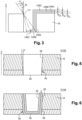
- FIG. 3 schematically illustrates the principle of this anisotropic deposition of the layer of ferroelectric material according to the invention.
- the cavity 50 is shown with a side wall 55 forming a zero angle with respect to the normal direction (parallel to the z axis) to the bottom wall 52.
- the principle described below applies in the same way for cavities whose side wall forms a non-zero angle with this normal direction with the bottom wall.
- the different thicknesses of the ferroelectric material layer are obtained using several unidirectional ion beam depositions, each oriented in a given direction.
- the layer of ferroelectric material is obtained by the deposition of a plurality of parts (at least two) forming, at the end, this layer of ferroelectric material 5.
- the deposition of each of these parts is carried out according to an associated deposition angle ⁇ 1 , ⁇ 2 , ⁇ 3 .
- Each deposition angle ⁇ 1 , ⁇ 2 , ⁇ 3 is defined with respect to a normal direction (parallel to the z axis) to the bottom wall 52 of the cavity 50.
- the deposition angles ⁇ 1 , ⁇ 2 , ⁇ 3 are here different from each other.
- each deposition angle ⁇ 1 , ⁇ 2 , ⁇ 3 is for example less than 90 degrees.
- each deposition angle ⁇ 1 , ⁇ 2 , ⁇ 3 is between 5 and 85 degrees.
- the ion beam making it possible to deposit each of these parts is arranged relative to the edge of the side wall 55 of the cavity 50. More particularly here, each ion beam is arranged relative to a corner C1 formed at the end of the side wall 55 of the cavity 50. More particularly, the ion beam concerned is directed towards the support layer and is partly cut because it crosses the corner C1 formed at the end of the side wall 55 of the cavity 50. The corner C1 then creates a shadowing effect by cutting the ion beam, thus making it possible to expose only certain areas of the cavity 50 to this ion beam.
- each ion beam (at an associated deposition angle) causes the deposition of the ferroelectric material on a specific area of the cavity 50.
- the characteristics associated with this ion beam make it possible to adjust the thickness of the portion of the deposited ferroelectric material layer 5.
- the thickness of each portion of the deposited ferroelectric material layer 5 depends, for example, here on the deposition speed and deposition time to form the ion beam concerned.
- the use of several deposition angles ⁇ 1 , ⁇ 2 , ⁇ 3 and the adjustment of the parameters of each ion beam then make it possible to carry out depositions in different zones of the cavity 50 but also to vary the thickness of the layer of ferroelectric material 5 in certain zones of the cavity 50.
- a deposition of a first part 105A of the ferroelectric material layer 5 is carried out according to a first deposition angle ⁇ 1 .
- the first part 105A is deposited on a part of the bottom wall 52 and a part of the side wall 55 of the cavity 50.
- This deposition of the first part 105A is carried out with a deposition speed and for a deposition duration making it possible to obtain a thickness e x1 for this first part 105A.
- a deposition of a second part 105B of the ferroelectric material layer 5 is carried out according to a second deposition angle ⁇ 2 .
- this second part 105B is also deposited on a part of the bottom wall 52 and a part of the side wall 55 of the cavity 50. More particularly, as shown in the Figure 3 , the second part 105B is, in part, deposited on the first layer 105A (which allows for the areas concerned to obtain a higher thickness of ferroelectric material).
- This deposition of the second part 105B is carried out with a deposition speed and for a deposition time making it possible to obtain a thickness e x2 for this second part 105B.
- the layer of ferroelectric material has a thickness of the order of the sum of the thickness e x1 and the thickness e x2 .
- the layer of ferroelectric material has the thickness e x2 .
- the areas not exposed to the ion beam emitted according to the second deposition angle ⁇ 2 are therefore devoid of this second part 105B (and for certain areas, which had not been subjected to the ion beam emitted according to the first deposition angle ⁇ 1 , they are, at this stage, completely devoid of ferroelectric material).
- the deposition of a third part 105C of the ferroelectric material layer 5 is carried out according to a third deposition angle ⁇ 3 .
- This third part 105C is also deposited on a part of the bottom wall 52 and a part of the side wall 55 of the cavity 50. More particularly, as shown in Figure 3 , the third part 105C is, in part, deposited on the second layer 105B (which allows for the areas concerned to obtain a higher thickness of ferroelectric material).
- This deposition of the third part 105C is carried out with a deposition speed and for a deposition time making it possible to obtain a thickness e x3 for this third part 105C.
- the layer of ferroelectric material has a thickness of the order of the sum of the thickness e x1 , the thickness e x2 and the thickness e x3 .
- the layer of ferroelectric material has (at this stage) a thickness of the order of the sum of the thickness e x2 and the thickness e x3 .
- the layer of ferroelectric material has the thickness e x3 .
- the areas not exposed to the ion beam emitted according to the third deposition angle ⁇ 3 are therefore devoid of this third part 105C (and for certain areas, which had not been subjected to the ion beam emitted according to the first deposition angle ⁇ 1 or emitted according to the second deposition angle ⁇ 2 , they are, at this stage, completely devoid of ferroelectric material).
- the example shown on the Figure 3 involves the emission of ion beams at three distinct deposition angles.
- the present invention is of course not limited to three deposition angles. There may be only two or more than three. Moreover, a generalization to a higher number of deposition angles makes it possible to obtain a quasi-continuous variation of the thickness of the layer of ferroelectric material in the cavity.
- the change in orientation of the ion beam (i.e. the modification of the deposition angle) is implemented by positioning the support layer 10 on a manufacturing support (not shown) and by tilting this manufacturing support so as to obtain the desired deposition angle.
- the manufacturing support can be rotated around an axis orthogonal to the bottom wall 52 of the cavity 50. This can be implemented regardless of the deposition method considered in the present invention.
- the change in orientation of the ion beam can be implemented by changing the orientation of the target from which the atoms are torn off (and which allows the ion beam to be formed) so as to obtain the different deposition angles sought.
- the method for manufacturing the ferroelectric storage device 1 then comprises, in step E106, a step E106a of depositing the first part 5A of the layer of ferroelectric material 5. This step is shown in the Figure 7 .
- a planarization step may be provided, after step E108.
- This planarization step is for example implemented by chemical mechanical polishing (or CMP for “ Chemical mechanical polishing” according to the commonly used acronym of Anglo-Saxon origin). Any other suitable method can be used (in particular masking methods).
- the manufacturing method may comprise, between step E106 of depositing the layer of ferroelectric material and step E108 of depositing the second layer, a step of implanting a doping element in the layer of ferroelectric material formed in step E106. This step then makes it possible to dope the layer of ferroelectric material with the doping element.
- Step E204 of depositing the first layer 2 therefore comprises two sub-steps here: a first sub-step E204a of depositing the first sub-layer 20 and a second sub-step E204b of depositing the second sub-layer 22.
- the first sub-layer 20 may be formed by cathode sputtering in a vacuum deposition chamber.
- the first sub-layer 20 is formed from titanium nitride, it is a reactive cathode sputtering.
- the second sub-layer 22 of the first layer 2 is deposited, in a conformal manner, on the first sub-layer 20 (step E204b).
- the second sub-layer 22 is for example formed by cathode sputtering in a vacuum deposition chamber.
- the second sub-layer 22 of the first layer 2 is formed in the same deposition chamber as the first sub-layer 20 of the first layer 2.
- the second sub-layer 22 is formed from titanium nitride, it is a reactive cathode sputtering.
- the deposition of the ferroelectric material layer 5 is, here too, carried out anisotropically. Furthermore, the deposition of the ferroelectric material layer 5 is here non-conformal.
- the layer of ferroelectric material 5 is deposited by a physical vapor deposition method (or PVD for “ Physical Vapor Deposition”).
- the layer of ferroelectric material 5 is deposited by an ion beam deposition (or IBD) method.
- the layer of ferroelectric material may be deposited by a method of Vacuum evaporation deposition. Similar deposition rates can be achieved using both vacuum evaporation and ion beam deposition.
- a crucible contains the material to be deposited. This crucible is heated by the Joule effect. By varying the current intensity, it is then possible to vary the deposition rate.
- the anisotropic character of the deposition is also based here on controlling the orientation of a target, from which atoms are torn off, relative to a substrate (here for example the support layer).
- the atoms torn off from the target then form an ion beam associated with a corresponding deposition direction.
- the anisotropic character of the deposition is associated with different deposition directions (using the deposition methods introduced previously).
- the method for manufacturing the ferroelectric storage device 1 then comprises, in step E206, a step E206a (similar to step E106a described previously) of deposition of the first part 5A of the layer of ferroelectric material 5.
- this first part 5A is deposited, in the cavity 50, according to a first deposition angle ⁇ 1 .
- This step E206a is implemented so as to obtain a thickness e 1 of ferroelectric material, for the first part 5A, in the cavity 50.
- the first part 5A is deposited at the bottom wall 52 of the cavity 50. This means that, in this second example of implementation of the manufacturing method according to the invention, the first deposition angle ⁇ 1 is substantially zero.
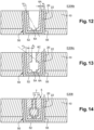
- Step E206 of depositing the layer of ferroelectric material 5 then comprises a step E206b of depositing a second part 6A of the layer of ferroelectric material 5. This step E206B is shown in the Figure 12 .
- this circular symmetry of the deposit can be ensured by a change in the orientation of the target from which the atoms are torn off (and which allow the ion beam to be formed).
- step E206 of depositing the layer of ferroelectric material 5 here comprises a step E206c (similar to step E106c described previously) of depositing a third part 6C of the layer of ferroelectric material 5. This step E206c is shown in the Figure 13 .
- This third part 6C is deposited in the cavity 50 at a third angle ⁇ 3 .
- This step E206c is implemented so as to obtain a third part 6C with a thickness e 3 (in the cavity 50).
- the third part 6C is deposited at the level of the side wall 55 of the cavity 50 (and even here at the level of the end of the side wall 55, opposite the bottom wall 52 of the cavity 50).
- the third deposition angle ⁇ 3 is therefore chosen here in order to allow deposition (by ion beam) only on the relevant area of the side wall 55 of the cavity 50.
- step E206c comprises for example the rotation of the manufacturing support (not shown) in order to ensure that the third part 6C is deposited on the relevant zone of the side wall 55 of the cavity 50. This can be implemented whatever the deposition method considered in the present invention.
- this circular symmetry of the deposit can be ensured by a change in the orientation of the target from which the atoms are torn off (and which allow the ion beam to be formed).
- the layer of ferroelectric material 5 is formed in the cavity 50.
- the layer of ferroelectric material 5 here comprises the first part 5A of thickness e 1 formed on the bottom wall 52 of the cavity 50, the second part 6A of thickness e 2 formed on the side wall 55 and on a part of the bottom wall of the cavity 50 and the third part 6C of thickness es formed on a part of the side wall 55 of the cavity 50.
- step E206c may be omitted if it is desired that the layer of ferroelectric material comprises only two different thicknesses.
- step E206 (as for step E106 described previously) may comprise additional steps corresponding to the deposition of additional parts of the layer of ferroelectric material at other thicknesses (these depositions being carried out according to other deposition angles).
- step E208 With the deposition of the second layer 7.
- This step E208 is shown in the figure 14 .
- This step is similar to step E108 described previously for the first example.
- the second layer 7 is formed on the layer of ferroelectric material 5 obtained at the end of step E206.
- the deposition of the second layer 7 is carried out in a compliant manner.
- the second layer 7 may here comprise a first sub-layer 70 and a second sub-layer 72.
- Step E208 of depositing the second layer 7 therefore here comprises two sub-steps: a first sub-step E208a of depositing the first sub-layer 70 and a second sub-step E208b of depositing the second sub-layer 72.
- the first sub-layer 70 is therefore first deposited, in a conformal manner, on the layer of ferroelectric material 5 (step E208a).
- the first sub-layer 70 is for example formed by cathode sputtering in a vacuum deposition chamber. In the case where the first sub-layer 70 is formed from titanium nitride, this is reactive cathode sputtering.
- the first sub-layer may be formed by chemical vapor deposition.
- the second sub-layer 72 of the second layer 7 is deposited, in a conforming manner, on the first sub-layer 70 (step E208b).
- the second sub-layer 72 is formed so as to fill all the remaining space in the cavity 50. This then makes it possible to obtain a ferroelectric storage device 1 completely integrated in the cavity 50 and without any protrusion or recession formed relative to the surface of the support layer 10.
- the assembly formed by the support layer 10 in which the ferroelectric storage device 1 is integrated therefore has a uniform surface.
- the second sub-layer 72 is for example formed by cathode sputtering in a vacuum deposition chamber.
- the second sub-layer 72 of the second layer 7 is formed in the same deposition chamber as the first sub-layer 70 of the second layer 7.
- the second sub-layer 72 is formed from titanium nitride, it is a reactive cathode sputtering.
- a planarization step may also be provided, after step E208.
- This planarization step is for example implemented by chemical mechanical polishing (or CMP for “ Chemical mechanical polishing ” according to the commonly used acronym of Anglo-Saxon origin). Any other suitable method may be used (in particular masking methods).
- This planarization step is particularly advantageous because, thanks to the standardization of the surface of the device 1, it makes it possible to improve the electrical performance of the ferroelectric storage device and to guarantee better quality of the interconnections.
- an encapsulation step may be provided after this planarization step.
- a connection to the second layer 7 may be implemented.
Landscapes
- Engineering & Computer Science (AREA)
- Manufacturing & Machinery (AREA)
- Chemical & Material Sciences (AREA)
- Materials Engineering (AREA)
- Semiconductor Memories (AREA)
- Formation Of Insulating Films (AREA)
- Chemical Vapour Deposition (AREA)
Applications Claiming Priority (1)
| Application Number | Priority Date | Filing Date | Title |
|---|---|---|---|
| FR2314898A FR3157785A1 (fr) | 2023-12-21 | 2023-12-21 | Dispositif de stockage ferroelectrique et procede de fabrication d’un tel dispositif |
Publications (1)
| Publication Number | Publication Date |
|---|---|
| EP4576984A1 true EP4576984A1 (de) | 2025-06-25 |
Family
ID=90904203
Family Applications (1)
| Application Number | Title | Priority Date | Filing Date |
|---|---|---|---|
| EP24222243.8A Pending EP4576984A1 (de) | 2023-12-21 | 2024-12-20 | Ferroelektrische speicheranordnung und verfahren zu ihrer herstellung |
Country Status (3)
| Country | Link |
|---|---|
| US (1) | US20250212704A1 (de) |
| EP (1) | EP4576984A1 (de) |
| FR (1) | FR3157785A1 (de) |
Citations (1)
| Publication number | Priority date | Publication date | Assignee | Title |
|---|---|---|---|---|
| WO2018194544A1 (en) * | 2017-04-17 | 2018-10-25 | Intel Corporation | Multi-bit ferroelectric memory |
-
2023
- 2023-12-21 FR FR2314898A patent/FR3157785A1/fr active Pending
-
2024
- 2024-12-20 US US18/990,667 patent/US20250212704A1/en active Pending
- 2024-12-20 EP EP24222243.8A patent/EP4576984A1/de active Pending
Patent Citations (1)
| Publication number | Priority date | Publication date | Assignee | Title |
|---|---|---|---|---|
| WO2018194544A1 (en) * | 2017-04-17 | 2018-10-25 | Intel Corporation | Multi-bit ferroelectric memory |
Non-Patent Citations (1)
| Title |
|---|
| LEE, DAESU ET AL., DANS ADVANCED MATERIALS, vol. 24, no. 3, 2012, pages 402 - 406 |
Also Published As
| Publication number | Publication date |
|---|---|
| US20250212704A1 (en) | 2025-06-26 |
| FR3157785A1 (fr) | 2025-06-27 |
Similar Documents
| Publication | Publication Date | Title |
|---|---|---|
| EP3210246B1 (de) | Verfahren zur herstellung einer widerstandsfähigen vorrichtung für einen speicher oder eine logische schaltung | |
| EP3012880B1 (de) | Nicht-flüchtige hybrid-speichervorrichtung, und herstellungsverfahren einer solchen vorrichtung | |
| EP4175448B1 (de) | Verfahren zur co-herstellung eines ferroelektrischen speichers und eines resistiven oxram-speichers und vorrichtung mit einem ferroelektrischen speicher und einem resistiven oxram-speicher | |
| FR3046290B1 (fr) | Methode de realisation d'espaceurs a faible permittivite | |
| EP1346405B1 (de) | Verfahren zur herstellung einer zwischen elektroden eingefügten inselstruktur und deren anwendung auf transistoren | |
| EP1801897B1 (de) | Verbessertes Verfahren zur Herstellung von Speicherzellen vom Typ PMC | |
| EP3506377B1 (de) | Elementarzelle, umfassend einen widerstandsspeicher und ein auswahlelement, ebene und matrix von ebenen umfassend eine vielzahl solcher zellen sowie zugeordnetes herstellungsverfahren | |
| EP3510644B1 (de) | Oxidbasierte resistive nichtflüchtige speicherzelle und verfahren zur herstellung davon | |
| EP4576984A1 (de) | Ferroelektrische speicheranordnung und verfahren zu ihrer herstellung | |
| EP3900043B1 (de) | Verfahren zur herstellung einer spintronic-vorrichtung mit einer dicken aktiven magnetischen schicht | |
| EP4576985A1 (de) | Ferroelektrische speicheranordnung und verfahren zur herstellung einer solchen | |
| EP4576980A1 (de) | Ferroelektrische speicheranordnung und verfahren zu ihrer herstellung | |
| EP2830086A1 (de) | Herstellungsverfahren eines Abstandshalters für elektronische Speicherzelle mit Doppel-Gate, und entsprechende elektronische Speicherzelle | |
| EP3843143B1 (de) | 3d-speicher und dessen herstellungsverfahren | |
| EP3965177A1 (de) | Resistiver speicher mit einer schaltzone zwischen zwei dielektrischen bereichen mit unterschiedlichen dotierungen und/oder dielektrizitätskonstanten | |
| EP2613342A2 (de) | Verfahren zur Herstellung einer nicht-flüchtigen Speicherzelle mit Doppel-Gate | |
| EP4142460A1 (de) | Resistive speichervorrichtung und ihr herstellungsverfahren | |
| EP4572593B1 (de) | Verfahren zur herstellung einer speichervorrichtung und eine speichervorrichtung | |
| EP4142451B1 (de) | Verfahren zur herstellung von resistiven speicherzellen | |
| WO2025022000A1 (fr) | Cellule mémoire résistive de type oxram et procédé de fabrication associé | |
| EP4062463B1 (de) | Oxram-speicherzelle mit niedriger formbildungsspannung und zugehöriges herstellungsverfahren | |
| EP3537489B1 (de) | Herstellungsverfahren einer durchlaufenden vorrichtung | |
| EP4391786A1 (de) | Eine phasenwechselspeichervorrichtung und ein verfahren zur herstellung einer phasenwechselspeichervorrichtung | |
| FR3157056A1 (fr) | Procédé de fabrication d’un cellule mémoire résistive de type OxRAM et cellule mémoire de type OxRAM associée |
Legal Events
| Date | Code | Title | Description |
|---|---|---|---|
| PUAI | Public reference made under article 153(3) epc to a published international application that has entered the european phase |
Free format text: ORIGINAL CODE: 0009012 |
|
| STAA | Information on the status of an ep patent application or granted ep patent |
Free format text: STATUS: REQUEST FOR EXAMINATION WAS MADE |
|
| 17P | Request for examination filed |
Effective date: 20241220 |
|
| AK | Designated contracting states |
Kind code of ref document: A1 Designated state(s): AL AT BE BG CH CY CZ DE DK EE ES FI FR GB GR HR HU IE IS IT LI LT LU LV MC ME MK MT NL NO PL PT RO RS SE SI SK SM TR |