EP4576946A2 - Erdungsoptimierung für ungeschirmte datenverbindungen - Google Patents
Erdungsoptimierung für ungeschirmte datenverbindungen Download PDFInfo
- Publication number
- EP4576946A2 EP4576946A2 EP24221862.6A EP24221862A EP4576946A2 EP 4576946 A2 EP4576946 A2 EP 4576946A2 EP 24221862 A EP24221862 A EP 24221862A EP 4576946 A2 EP4576946 A2 EP 4576946A2
- Authority
- EP
- European Patent Office
- Prior art keywords
- ground connections
- plane
- differential signal
- signal trace
- ground
- Prior art date
- Legal status (The legal status is an assumption and is not a legal conclusion. Google has not performed a legal analysis and makes no representation as to the accuracy of the status listed.)
- Pending
Links
Images





Classifications
-
- H—ELECTRICITY
- H05—ELECTRIC TECHNIQUES NOT OTHERWISE PROVIDED FOR
- H05K—PRINTED CIRCUITS; CASINGS OR CONSTRUCTIONAL DETAILS OF ELECTRIC APPARATUS; MANUFACTURE OF ASSEMBLAGES OF ELECTRICAL COMPONENTS
- H05K1/00—Printed circuits
- H05K1/02—Details
- H05K1/0213—Electrical arrangements not otherwise provided for
- H05K1/0216—Reduction of cross-talk, noise or electromagnetic interference
- H05K1/0218—Reduction of cross-talk, noise or electromagnetic interference by printed shielding conductors, ground planes or power plane
- H05K1/0224—Patterned shielding planes, ground planes or power planes
- H05K1/0227—Split or nearly split shielding or ground planes
-
- H—ELECTRICITY
- H05—ELECTRIC TECHNIQUES NOT OTHERWISE PROVIDED FOR
- H05K—PRINTED CIRCUITS; CASINGS OR CONSTRUCTIONAL DETAILS OF ELECTRIC APPARATUS; MANUFACTURE OF ASSEMBLAGES OF ELECTRICAL COMPONENTS
- H05K1/00—Printed circuits
- H05K1/02—Details
- H05K1/0213—Electrical arrangements not otherwise provided for
- H05K1/0216—Reduction of cross-talk, noise or electromagnetic interference
-
- H—ELECTRICITY
- H05—ELECTRIC TECHNIQUES NOT OTHERWISE PROVIDED FOR
- H05K—PRINTED CIRCUITS; CASINGS OR CONSTRUCTIONAL DETAILS OF ELECTRIC APPARATUS; MANUFACTURE OF ASSEMBLAGES OF ELECTRICAL COMPONENTS
- H05K1/00—Printed circuits
- H05K1/02—Details
- H05K1/0213—Electrical arrangements not otherwise provided for
- H05K1/0215—Grounding of printed circuits by connection to external grounding means
-
- H—ELECTRICITY
- H05—ELECTRIC TECHNIQUES NOT OTHERWISE PROVIDED FOR
- H05K—PRINTED CIRCUITS; CASINGS OR CONSTRUCTIONAL DETAILS OF ELECTRIC APPARATUS; MANUFACTURE OF ASSEMBLAGES OF ELECTRICAL COMPONENTS
- H05K1/00—Printed circuits
- H05K1/02—Details
- H05K1/0213—Electrical arrangements not otherwise provided for
- H05K1/0237—High frequency adaptations
- H05K1/0245—Lay-out of balanced signal pairs, e.g. differential lines or twisted lines
-
- H—ELECTRICITY
- H05—ELECTRIC TECHNIQUES NOT OTHERWISE PROVIDED FOR
- H05K—PRINTED CIRCUITS; CASINGS OR CONSTRUCTIONAL DETAILS OF ELECTRIC APPARATUS; MANUFACTURE OF ASSEMBLAGES OF ELECTRICAL COMPONENTS
- H05K1/00—Printed circuits
- H05K1/18—Printed circuits structurally associated with non-printed electric components
- H05K1/181—Printed circuits structurally associated with non-printed electric components associated with surface mounted components
-
- H—ELECTRICITY
- H05—ELECTRIC TECHNIQUES NOT OTHERWISE PROVIDED FOR
- H05K—PRINTED CIRCUITS; CASINGS OR CONSTRUCTIONAL DETAILS OF ELECTRIC APPARATUS; MANUFACTURE OF ASSEMBLAGES OF ELECTRICAL COMPONENTS
- H05K1/00—Printed circuits
- H05K1/02—Details
- H05K1/0213—Electrical arrangements not otherwise provided for
- H05K1/0216—Reduction of cross-talk, noise or electromagnetic interference
- H05K1/023—Reduction of cross-talk, noise or electromagnetic interference using auxiliary mounted passive components or auxiliary substances
- H05K1/0231—Capacitors or dielectric substances
-
- H—ELECTRICITY
- H05—ELECTRIC TECHNIQUES NOT OTHERWISE PROVIDED FOR
- H05K—PRINTED CIRCUITS; CASINGS OR CONSTRUCTIONAL DETAILS OF ELECTRIC APPARATUS; MANUFACTURE OF ASSEMBLAGES OF ELECTRICAL COMPONENTS
- H05K2201/00—Indexing scheme relating to printed circuits covered by H05K1/00
- H05K2201/03—Conductive materials
- H05K2201/0332—Structure of the conductor
- H05K2201/0388—Other aspects of conductors
- H05K2201/0394—Conductor crossing over a hole in the substrate or a gap between two separate substrate parts
-
- H—ELECTRICITY
- H05—ELECTRIC TECHNIQUES NOT OTHERWISE PROVIDED FOR
- H05K—PRINTED CIRCUITS; CASINGS OR CONSTRUCTIONAL DETAILS OF ELECTRIC APPARATUS; MANUFACTURE OF ASSEMBLAGES OF ELECTRICAL COMPONENTS
- H05K2201/00—Indexing scheme relating to printed circuits covered by H05K1/00
- H05K2201/09—Shape and layout
- H05K2201/09209—Shape and layout details of conductors
- H05K2201/0929—Conductive planes
- H05K2201/093—Layout of power planes, ground planes or power supply conductors, e.g. having special clearance holes therein
-
- H—ELECTRICITY
- H05—ELECTRIC TECHNIQUES NOT OTHERWISE PROVIDED FOR
- H05K—PRINTED CIRCUITS; CASINGS OR CONSTRUCTIONAL DETAILS OF ELECTRIC APPARATUS; MANUFACTURE OF ASSEMBLAGES OF ELECTRICAL COMPONENTS
- H05K2201/00—Indexing scheme relating to printed circuits covered by H05K1/00
- H05K2201/09—Shape and layout
- H05K2201/09209—Shape and layout details of conductors
- H05K2201/09654—Shape and layout details of conductors covering at least two types of conductors provided for in H05K2201/09218 - H05K2201/095
- H05K2201/09663—Divided layout, i.e. conductors divided in two or more parts
-
- H—ELECTRICITY
- H05—ELECTRIC TECHNIQUES NOT OTHERWISE PROVIDED FOR
- H05K—PRINTED CIRCUITS; CASINGS OR CONSTRUCTIONAL DETAILS OF ELECTRIC APPARATUS; MANUFACTURE OF ASSEMBLAGES OF ELECTRICAL COMPONENTS
- H05K2201/00—Indexing scheme relating to printed circuits covered by H05K1/00
- H05K2201/09—Shape and layout
- H05K2201/09209—Shape and layout details of conductors
- H05K2201/09654—Shape and layout details of conductors covering at least two types of conductors provided for in H05K2201/09218 - H05K2201/095
- H05K2201/0979—Redundant conductors or connections, i.e. more than one current path between two points
-
- H—ELECTRICITY
- H05—ELECTRIC TECHNIQUES NOT OTHERWISE PROVIDED FOR
- H05K—PRINTED CIRCUITS; CASINGS OR CONSTRUCTIONAL DETAILS OF ELECTRIC APPARATUS; MANUFACTURE OF ASSEMBLAGES OF ELECTRICAL COMPONENTS
- H05K2201/00—Indexing scheme relating to printed circuits covered by H05K1/00
- H05K2201/09—Shape and layout
- H05K2201/09818—Shape or layout details not covered by a single group of H05K2201/09009 - H05K2201/09809
- H05K2201/09972—Partitioned, e.g. portions of a PCB dedicated to different functions; Boundary lines therefore; Portions of a PCB being processed separately or differently
-
- H—ELECTRICITY
- H05—ELECTRIC TECHNIQUES NOT OTHERWISE PROVIDED FOR
- H05K—PRINTED CIRCUITS; CASINGS OR CONSTRUCTIONAL DETAILS OF ELECTRIC APPARATUS; MANUFACTURE OF ASSEMBLAGES OF ELECTRICAL COMPONENTS
- H05K2201/00—Indexing scheme relating to printed circuits covered by H05K1/00
- H05K2201/10—Details of components or other objects attached to or integrated in a printed circuit board
- H05K2201/10007—Types of components
- H05K2201/10015—Non-printed capacitor
-
- H—ELECTRICITY
- H05—ELECTRIC TECHNIQUES NOT OTHERWISE PROVIDED FOR
- H05K—PRINTED CIRCUITS; CASINGS OR CONSTRUCTIONAL DETAILS OF ELECTRIC APPARATUS; MANUFACTURE OF ASSEMBLAGES OF ELECTRICAL COMPONENTS
- H05K2201/00—Indexing scheme relating to printed circuits covered by H05K1/00
- H05K2201/10—Details of components or other objects attached to or integrated in a printed circuit board
- H05K2201/10007—Types of components
- H05K2201/10189—Non-printed connector
-
- H—ELECTRICITY
- H05—ELECTRIC TECHNIQUES NOT OTHERWISE PROVIDED FOR
- H05K—PRINTED CIRCUITS; CASINGS OR CONSTRUCTIONAL DETAILS OF ELECTRIC APPARATUS; MANUFACTURE OF ASSEMBLAGES OF ELECTRICAL COMPONENTS
- H05K2201/00—Indexing scheme relating to printed circuits covered by H05K1/00
- H05K2201/10—Details of components or other objects attached to or integrated in a printed circuit board
- H05K2201/10431—Details of mounted components
- H05K2201/10507—Involving several components
- H05K2201/10545—Related components mounted on both sides of the PCB
Definitions
- This disclosure relates to unshielded data connections in a high interference network, such as an automotive network. More particularly, this disclosure relates to grounding techniques to reduce interference on unshielded data connections.
- unshielded twisted pair (UTP) cables are often used for communication with physical layer transceiver (PHY) system-on-a-chip (SoC) devices with speeds up to 1 Gbps.
- PHY physical layer transceiver
- SoC system-on-a-chip
- UTP cables are also often implemented for switch SoC devices with integrated PHY ports with speeds up to 1000BT1.
- MDIs Medium dependent interfaces
- MDIs serve as the connection point between devices and the transmission medium, such as copper cables or optical fibers.
- An MDI is a physical interface that connects a device to the transmission medium used for data communication, such as copper wires, optical fibers, or wireless channels.
- the MDI serves as the critical boundary where the electrical or optical signals generated by the device are adapted for propagation through the chosen transmission medium.
- MDIs are integral components of communication systems and are typically designed to comply with established standards, such as IEEE 802.3 for Ethernet, ensuring compatibility and interoperability between different devices.
- MDIs are defined by their physical connectors, electrical or optical signaling specifications, and impedance matching capabilities. MDIs are often equipped with mechanisms to handle medium-specific challenges, such as electromagnetic interference in copper-based systems or modal dispersion in optical fiber systems. In addition to signal transmission, MDIs may incorporate features for signal conditioning, such as amplification, filtering, or equalization, to maintain data integrity over various distances and media types. Depending on the application, MDIs can also include protection circuits, grounding provisions, and isolation mechanisms to safeguard devices from transient voltages, surges, or ground loops. These interfaces play a pivotal role in enabling reliable and efficient data transfer in both wired and wireless communication systems.
- MDI grounding connection schemes have significant impacts on the electromagnetic interference performance of automotive networks with UTP cable channels.
- Unshielded cable channels i.e., UTP cables
- MDI grounding can have a negative impact on UTP cables if not implemented correctly.
- the interaction between MDI grounding and UTP cables affects the susceptibility of the UTP cable to noise. Improper grounding at the MDI can introduce common-mode noise into the UTP cable. Since UTP cables lack shielding, they are more vulnerable to noise if the grounding is not properly managed. This noise can degrade the differential signals transmitted through the twisted pairs, leading to errors or reduced data rates.
- MDI grounding can also affect ground loops. Ground loops occur when there are differences in ground potential between interconnected devices, creating a loop where unintended current flows. With UTP cables, ground loops can induce interference into the signal, as the cable does not have a shield to isolate the twisted pairs from external electrical disturbances.
- the unshielded data connection may be a differential signal trace pair disposed on a first surface of a printed circuitry board (PCB), the PCB having a major plane.
- the differential signal trace pair is disposed within an imaginary plane, perpendicular to the surface of the PCB, that includes the differential signal trace pair as a line segment within the imaginary plane.
- a symmetrical arrangement of one or more ground connections is disposed around the differential signal trace pair. The arrangement is symmetrical with respect to the imaginary plane.
- a first half of the ground connections may be disposed to one side of the imaginary plane while a second half of the ground connections may be disposed to the other side of the imaginary plane.
- a first half of the ground connections of an even-numbered subset of the odd number of ground connections may be disposed on a first surface of the PCB to one side of the imaginary plane while a second half of the ground connections of the even-numbered subset are disposed on the first surface of the PCB to the other side of the imaginary plane.
- a first ground connection is disposed on a second surface of the PCB at a location that intersects the imaginary plane. The rest of the remaining number of ground connections, being an even number of ground connections, are disposed on the second surface of the PCB, distributed symmetrically with respect to the imaginary plane.
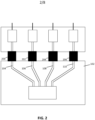
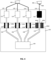
- Signal source 100 is disposed in a first area 136 of PCB 102.
- Area 136 may comprise a first ground plane for digital logic disposed on PCB 102.
- MDI ports 112, 114,116, and 118 are disposed in a second area 138 of PCB 102.
- Area 138 may comprise a second ground plane for the cable connection made via the MDI ports.
- Discontinuity 140 on the surface or in the ground plane layer of PCB 102 is used for electrically isolating between area 136 and area 138.
- Discontinuity 140 may be formed, for example, by etching or otherwise removing part of a metal layer so as to create a gap between different ground regions.
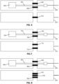
- FIG. 8 is an illustrative diagram of a second symmetrical arrangement of an odd number of ground connections disposed on different surfaces of a printed circuit board, in accordance with some implementations of the subject matter of this disclosure.
- FIG. 8 depicts two opposing surfaces 804 and 810 of a PCB.
- Signal source 800 and differential signal trace pair 802 are disposed on a first surface 804 of a PCB.
- Ground connections 806 and 808 are also disposed on first surface 804 and arranged symmetrically to either side of an imaginary plane perpendicular to surface 804 that includes differential signal trace pair 802 as a line segment within the imaginary plane.
- ground connections 812, 814, and 816 are also disposed symmetrically to either side of the imaginary plane, which is to say that the imaginary plane intersects ground connection 814 at its midpoint such that half of ground connection 814 is disposed to either side of the imaginary plane.
- Ground connections 812 and 816 are disposed at equidistant locations to either side of the imaginary plane.
- the distance between ground connection 812 and ground connection 816 need not be identical to the distance between ground connection 806 and ground connection 808, so long as each pair of ground connections is disposed symmetrically with respect to the imaginary plane, or with respect to a portion of the differential signal trace pair that forms a line segments within the imaginary plane.
- FIG. 9 is an illustrative diagram of a symmetrical arrangement of an odd number of ground connections disposed on different surfaces and within at least on interior layer of a printed circuit board, in accordance with some implementations of the subject matter of this disclosure.
- Signal source 900 and differential signal trace pair 902 are disposed on a first surface 904 of a PCB.
- Ground connections 906 and 908 are also disposed on first surface 904 and arranged symmetrically to either side of an imaginary plane 910 perpendicular to surface 904 that includes differential signal trace pair 902 as a line segment within the imaginary plane.
- Ground connection 912 is then disposed on an interior layer 914 of the PCB at a location such that imaginary plane 910 intersects ground connection 912 at its midpoint, with half of ground connection 912 is disposed to either side of the imaginary plane.
- ground connections 918 and 920 are also disposed symmetrically with respect to imaginary plane 910.
- the distance between ground connection 918 and ground connection 920 need not be identical to the distance between ground connection 906 and ground connection 908, so long as each pair of ground connections is disposed symmetrically with respect to imaginary plane 910.
- FIG. 10 is a flow diagram representing an illustrative process for shielding a differential signal trace pair using a symmetrical arrangement of ground connections, in accordance with some implementations of the subject matter of this disclosure.
- a counter variable N is initialized with an initial value of 1.
- a variable T D is also initialized, representing the number of differential signal trace pairs for which ground connections must be disposed in a respective symmetrical arrangement.
- T G is initialized, representing the number of ground connections to be disposed in a symmetrical arrangement around the N th differential signal trace pair.
- T G is an odd number using, e.g., a modulus function to determine whether the remainder that results from dividing T G by 2 is equal to 1.
- T G is and odd number ("Yes") at 1006, then, at 1008, a first ground connection is disposed at a location that intersects an imaginary plane that includes the N th differential signal trace pair as a line segment in the imaginary plane. Then, at 1010, the value of a variable H is set to half of the remaining number of ground connections (i.e., half of one less than T G ). If T G is an even number ("No" at 1006), then, at 1012, the value of H is set to half of T G .
- H ground connections are disposed to a first side of the imaginary plane. H ground connections are also disposed to a second side of the imaginary plane. Each pair of ground connections may be disposed on the same surface of a PCB as the N th differential signal trace pair, or an opposing surface of the PCB.
Landscapes
- Engineering & Computer Science (AREA)
- Microelectronics & Electronic Packaging (AREA)
- Physics & Mathematics (AREA)
- Electromagnetism (AREA)
- Structure Of Printed Boards (AREA)
- Coupling Device And Connection With Printed Circuit (AREA)
- Multi-Conductor Connections (AREA)
Applications Claiming Priority (2)
| Application Number | Priority Date | Filing Date | Title |
|---|---|---|---|
| US202363612335P | 2023-12-19 | 2023-12-19 | |
| US18/985,837 US20250203754A1 (en) | 2023-12-19 | 2024-12-18 | Grounding optimization for unshielded data connections |
Publications (2)
| Publication Number | Publication Date |
|---|---|
| EP4576946A2 true EP4576946A2 (de) | 2025-06-25 |
| EP4576946A3 EP4576946A3 (de) | 2025-09-10 |
Family
ID=93925793
Family Applications (1)
| Application Number | Title | Priority Date | Filing Date |
|---|---|---|---|
| EP24221862.6A Pending EP4576946A3 (de) | 2023-12-19 | 2024-12-19 | Erdungsoptimierung für ungeschirmte datenverbindungen |
Country Status (3)
| Country | Link |
|---|---|
| US (1) | US20250203754A1 (de) |
| EP (1) | EP4576946A3 (de) |
| CN (1) | CN120186865A (de) |
Family Cites Families (2)
| Publication number | Priority date | Publication date | Assignee | Title |
|---|---|---|---|---|
| WO2011056977A2 (en) * | 2009-11-06 | 2011-05-12 | Molex Incorporated | Multi-layer circuit member and assembly therefor |
| US20210392742A1 (en) * | 2020-06-11 | 2021-12-16 | Innogrit Technologies Co., Ltd. | Embedded microstrip with open slot for high speed signal traces |
-
2024
- 2024-12-18 US US18/985,837 patent/US20250203754A1/en active Pending
- 2024-12-19 CN CN202411883288.1A patent/CN120186865A/zh active Pending
- 2024-12-19 EP EP24221862.6A patent/EP4576946A3/de active Pending
Also Published As
| Publication number | Publication date |
|---|---|
| EP4576946A3 (de) | 2025-09-10 |
| US20250203754A1 (en) | 2025-06-19 |
| CN120186865A (zh) | 2025-06-20 |
Similar Documents
| Publication | Publication Date | Title |
|---|---|---|
| US8284007B1 (en) | Magnetic package for a communication system | |
| KR100984998B1 (ko) | 다른 쌍들에 누화 보상을 배치함으로써 야기되는 근단 누화 불균형 보정 | |
| US20080024939A1 (en) | Communication system for hazardous environments | |
| US6729899B2 (en) | Balance high density 110 IDC terminal block | |
| US20110235229A1 (en) | Ethernet surge protector | |
| PH12014501769B1 (en) | High speed communication jack | |
| US8076990B2 (en) | Communications medium connector with integrated common-mode noise suppression | |
| US11711591B2 (en) | Common-mode filtering for high-speed cable interface | |
| WO2018171241A1 (zh) | 双屏蔽层的usb连接器 | |
| CN114915507B (zh) | 一种千兆poe供电通信电路 | |
| Kugelstadt | The RS-485 Design Guide: A short compendium for robust data transmission design | |
| JP2000123925A (ja) | 容量性プレ―ト付きモジュラコネクタ | |
| JP4241772B2 (ja) | プリント回路板および差動信号伝送構造 | |
| EP4576946A2 (de) | Erdungsoptimierung für ungeschirmte datenverbindungen | |
| US8243412B2 (en) | Surge protection systems and methods for outside plant ethernet | |
| JP7675357B2 (ja) | 電子制御装置 | |
| JP2009135760A (ja) | 低放射ノイズ電子機器、プラグまたはアダプタ付伝送線路接続ケーブル、および電子機器の放射ノイズ除去方法 | |
| US8878630B2 (en) | Common-mode noise suppression filter | |
| CN220775394U (zh) | 一种防雷击电路、模块、电路板及电子设备 | |
| US11395401B1 (en) | Printed circuit board structure and method for improved electromagnetic compatibility performance | |
| EP4618432A1 (de) | Drahtlose kommunikationsvorrichtung und drahtloses system | |
| US20150318082A1 (en) | Signal and Drain Arrangement for High Speed Cables | |
| KR20230166945A (ko) | 서보 앰프 | |
| TWI677206B (zh) | 可避免雷擊突波造成實體層電路當機的乙太網路通信電路 | |
| AU2017101132A4 (en) | Connector system impedance matching |
Legal Events
| Date | Code | Title | Description |
|---|---|---|---|
| PUAI | Public reference made under article 153(3) epc to a published international application that has entered the european phase |
Free format text: ORIGINAL CODE: 0009012 |
|
| STAA | Information on the status of an ep patent application or granted ep patent |
Free format text: STATUS: THE APPLICATION HAS BEEN PUBLISHED |
|
| AK | Designated contracting states |
Kind code of ref document: A2 Designated state(s): AL AT BE BG CH CY CZ DE DK EE ES FI FR GB GR HR HU IE IS IT LI LT LU LV MC ME MK MT NL NO PL PT RO RS SE SI SK SM TR |
|
| PUAL | Search report despatched |
Free format text: ORIGINAL CODE: 0009013 |
|
| AK | Designated contracting states |
Kind code of ref document: A3 Designated state(s): AL AT BE BG CH CY CZ DE DK EE ES FI FR GB GR HR HU IE IS IT LI LT LU LV MC ME MK MT NL NO PL PT RO RS SE SI SK SM TR |
|
| RIC1 | Information provided on ipc code assigned before grant |
Ipc: H05K 1/02 20060101AFI20250806BHEP |
|
| RAP1 | Party data changed (applicant data changed or rights of an application transferred) |
Owner name: INFINEON TECHNOLOGIES AMERICAS CORP. |
|
| STAA | Information on the status of an ep patent application or granted ep patent |
Free format text: STATUS: REQUEST FOR EXAMINATION WAS MADE |
|
| 17P | Request for examination filed |
Effective date: 20260310 |