EP4576531A1 - Elektronische vorrichtung und verfahren zur steuerung eines elektrischen energiewandlers mit synchronisiertem dreiecksignal und stromwandlersystem dafür - Google Patents
Elektronische vorrichtung und verfahren zur steuerung eines elektrischen energiewandlers mit synchronisiertem dreiecksignal und stromwandlersystem dafür Download PDFInfo
- Publication number
- EP4576531A1 EP4576531A1 EP24221235.5A EP24221235A EP4576531A1 EP 4576531 A1 EP4576531 A1 EP 4576531A1 EP 24221235 A EP24221235 A EP 24221235A EP 4576531 A1 EP4576531 A1 EP 4576531A1
- Authority
- EP
- European Patent Office
- Prior art keywords
- resonator
- voltage
- ramp
- control
- switch
- Prior art date
- Legal status (The legal status is an assumption and is not a legal conclusion. Google has not performed a legal analysis and makes no representation as to the accuracy of the status listed.)
- Pending
Links
Images


Classifications
-
- H—ELECTRICITY
- H02—GENERATION; CONVERSION OR DISTRIBUTION OF ELECTRIC POWER
- H02M—APPARATUS FOR CONVERSION BETWEEN AC AND AC, BETWEEN AC AND DC, OR BETWEEN DC AND DC, AND FOR USE WITH MAINS OR SIMILAR POWER SUPPLY SYSTEMS; CONVERSION OF DC OR AC INPUT POWER INTO SURGE OUTPUT POWER; CONTROL OR REGULATION THEREOF
- H02M3/00—Conversion of DC power input into DC power output
- H02M3/22—Conversion of DC power input into DC power output with intermediate conversion into AC
- H02M3/24—Conversion of DC power input into DC power output with intermediate conversion into AC by static converters
- H02M3/28—Conversion of DC power input into DC power output with intermediate conversion into AC by static converters using discharge tubes with control electrode or semiconductor devices with control electrode to produce the intermediate AC
- H02M3/325—Conversion of DC power input into DC power output with intermediate conversion into AC by static converters using discharge tubes with control electrode or semiconductor devices with control electrode to produce the intermediate AC using devices of a triode or a transistor type requiring continuous application of a control signal
- H02M3/335—Conversion of DC power input into DC power output with intermediate conversion into AC by static converters using discharge tubes with control electrode or semiconductor devices with control electrode to produce the intermediate AC using devices of a triode or a transistor type requiring continuous application of a control signal using semiconductor devices only
- H02M3/33569—Conversion of DC power input into DC power output with intermediate conversion into AC by static converters using discharge tubes with control electrode or semiconductor devices with control electrode to produce the intermediate AC using devices of a triode or a transistor type requiring continuous application of a control signal using semiconductor devices only having several active switching elements
-
- H—ELECTRICITY
- H02—GENERATION; CONVERSION OR DISTRIBUTION OF ELECTRIC POWER
- H02M—APPARATUS FOR CONVERSION BETWEEN AC AND AC, BETWEEN AC AND DC, OR BETWEEN DC AND DC, AND FOR USE WITH MAINS OR SIMILAR POWER SUPPLY SYSTEMS; CONVERSION OF DC OR AC INPUT POWER INTO SURGE OUTPUT POWER; CONTROL OR REGULATION THEREOF
- H02M1/00—Details of apparatus for conversion
- H02M1/08—Circuits specially adapted for the generation of control voltages for semiconductor devices incorporated in static converters
- H02M1/088—Circuits specially adapted for the generation of control voltages for semiconductor devices incorporated in static converters for the simultaneous control of series or parallel connected semiconductor devices
-
- H—ELECTRICITY
- H02—GENERATION; CONVERSION OR DISTRIBUTION OF ELECTRIC POWER
- H02M—APPARATUS FOR CONVERSION BETWEEN AC AND AC, BETWEEN AC AND DC, OR BETWEEN DC AND DC, AND FOR USE WITH MAINS OR SIMILAR POWER SUPPLY SYSTEMS; CONVERSION OF DC OR AC INPUT POWER INTO SURGE OUTPUT POWER; CONTROL OR REGULATION THEREOF
- H02M11/00—Power conversion systems not covered by the preceding groups
-
- H—ELECTRICITY
- H02—GENERATION; CONVERSION OR DISTRIBUTION OF ELECTRIC POWER
- H02M—APPARATUS FOR CONVERSION BETWEEN AC AND AC, BETWEEN AC AND DC, OR BETWEEN DC AND DC, AND FOR USE WITH MAINS OR SIMILAR POWER SUPPLY SYSTEMS; CONVERSION OF DC OR AC INPUT POWER INTO SURGE OUTPUT POWER; CONTROL OR REGULATION THEREOF
- H02M3/00—Conversion of DC power input into DC power output
- H02M3/01—Resonant DC/DC converters
-
- H—ELECTRICITY
- H02—GENERATION; CONVERSION OR DISTRIBUTION OF ELECTRIC POWER
- H02M—APPARATUS FOR CONVERSION BETWEEN AC AND AC, BETWEEN AC AND DC, OR BETWEEN DC AND DC, AND FOR USE WITH MAINS OR SIMILAR POWER SUPPLY SYSTEMS; CONVERSION OF DC OR AC INPUT POWER INTO SURGE OUTPUT POWER; CONTROL OR REGULATION THEREOF
- H02M3/00—Conversion of DC power input into DC power output
- H02M3/22—Conversion of DC power input into DC power output with intermediate conversion into AC
- H02M3/24—Conversion of DC power input into DC power output with intermediate conversion into AC by static converters
- H02M3/28—Conversion of DC power input into DC power output with intermediate conversion into AC by static converters using discharge tubes with control electrode or semiconductor devices with control electrode to produce the intermediate AC
- H02M3/325—Conversion of DC power input into DC power output with intermediate conversion into AC by static converters using discharge tubes with control electrode or semiconductor devices with control electrode to produce the intermediate AC using devices of a triode or a transistor type requiring continuous application of a control signal
- H02M3/335—Conversion of DC power input into DC power output with intermediate conversion into AC by static converters using discharge tubes with control electrode or semiconductor devices with control electrode to produce the intermediate AC using devices of a triode or a transistor type requiring continuous application of a control signal using semiconductor devices only
- H02M3/33569—Conversion of DC power input into DC power output with intermediate conversion into AC by static converters using discharge tubes with control electrode or semiconductor devices with control electrode to produce the intermediate AC using devices of a triode or a transistor type requiring continuous application of a control signal using semiconductor devices only having several active switching elements
- H02M3/33573—Full-bridge at primary side of an isolation transformer
Definitions
- the present invention relates to an electronic device for controlling an electrical energy converter capable of converting an input voltage into an output voltage.
- the invention also relates to an electrical energy conversion system comprising such a converter and such an electronic device for controlling the converter.
- the invention also relates to a method for controlling such a converter.
- a converter comprising two input terminals for receiving the input voltage, two output terminals for delivering the output voltage, a resonator, and several switches connected to the resonator, the resonator resonating following successive resonance cycles, each resonance cycle having a duration equal to a resonance period, the resonance period being equal to the inverse of an oscillation frequency of the resonator.
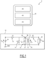
- the electronic electrical energy conversion system 5 is typically a system for converting into direct electrical energy, such as a direct-to-direct conversion system capable of converting a first direct electrical energy received at the input into a second direct electrical energy delivered at the output, or even an alternating-to-direct conversion system capable of converting alternating electrical energy received at the input into direct electrical energy delivered at the output of the conversion system 5.
- the electrical energy conversion system 5 preferably further comprises a voltage rectifier, not shown, connected to the input of the electrical energy converter 10 and capable of rectifying the AC electrical voltage received at the input of the conversion system 5 to deliver a rectified electrical voltage at the input of the converter 10, the electrical energy converter 10 preferably being a DC-DC converter capable of converting DC electrical energy into another DC electrical energy.
- the voltage rectifier is for example a rectifier bridge, such as a diode bridge.
- the voltage rectifier is formed in part by switches of the converter 10.
- the electrical energy converter 10 is preferably a DC-DC converter, and is also called a DC-DC converter.
- the DC-DC converter generally has the role of regulating a supply voltage V out of a load 22 to a stable value, by being powered by an energy source 24 providing a substantially DC voltage V in .
- the energy source 24 is for example a battery or a solar panel.
- the electrical energy converter 10 is then configured to raise the value of the direct voltage between its input and its output, and is then also called a step-up direct-direct converter, or even a high-step-up direct-direct converter; or is configured to lower the value of the direct voltage between its input and its output, and is then called a step-down DC-DC converter, with also a variant of a deep step-down DC-DC converter.
- the value of the input voltage typically corresponds to the voltage V in of the energy source 24, and the value of the output voltage corresponds to the voltage V out at the terminals of the load 22, the voltage V in then being greater than the voltage V out .
- the value of the input voltage also typically corresponds to the voltage V in of the energy source 24, and the value of the output voltage corresponds to the voltage V out at the terminals of the load 22, the voltage V in then being lower than the voltage V out .
- the value of the input voltage corresponds for example to the voltage difference (V in -V out ), and the value of the output voltage corresponds for example to the voltage V out , the voltage difference (V in -V out ) being significantly greater than the voltage V out .
- the value of the input voltage corresponds for example to the voltage difference (V in -V out ), and the value of the output voltage corresponds to the voltage V out at the terminals of the load 22, the voltage difference (V in -V out ) being greater than the voltage V out .
- the converter 10 comprises several switches 14 capable of being controlled to alternate phases at substantially constant voltage and phases at substantially constant load at the terminals of the resonator 12.
- This alternation of phases at substantially constant voltage and phases at substantially constant load is typically carried out within periods of substantially constant duration corresponding to the operating frequency of the converter 10, depending on an oscillation frequency, also called natural frequency or vibration frequency, of the resonator 12.
- the phases at substantially constant load make it possible, in steady state or permanent operation, to pass from one constant voltage to another and to close the switches which must be closed when the voltage at their terminals is preferably zero in order to have a so-called zero voltage switching, also called ZVS switching (from the English Zero Voltage Switching).
- Each switch 14 comprises, for example, a transistor and an antiparallel diode (not shown) intrinsic to the transistor.
- the transistor is, for example, an insulated gate field effect transistor, also called a MOSFET (from the English Metal Oxide Semiconductor Field Effect Transistor ) .
- the transistor is a bipolar transistor; an insulated gate bipolar transistor, also called IGBT (from the English Insulated Gate Bipolar Transistor ); a silicon (Si) based transistor, a GaN (from the English Gallium Nitride ) based transistor ; a silicon carbide (SiC) based transistor, or a diamond based transistor, or a thyristor, or a mechanical switch, such as a MEMS (from the English MicroElectroMechanical System) micro-switch.
- IGBT from the English Insulated Gate Bipolar Transistor
- Si silicon
- GaN from the English Gallium Nitride
- SiC silicon carbide
- Diamond thyristor or a mechanical switch, such as a MEMS (from the English MicroElectroMechanical System) micro-switch.
- substantially constant charge is meant an exchange of a charge with the outside which is less than 30% of the charge which would have been exchanged with the outside if the voltage had been kept constant.
- substantially constant charge is meant a variation in charge less than 30% of the charge which would have been exchanged with the outside of the resonator 12 if the voltage across the terminals of the resonator 12 had been kept constant over the time period considered.
- substantially open electrical circuit means a circuit in which a possible leakage current leads to a variation in charge of the resonator 12 of less than 30% of the charge which would have been exchanged with the exterior of the resonator 12 if the voltage across the terminals of the resonator 12 had been kept constant over the time period considered.
- substantially constant voltage is meant a voltage variation of less than 20%, preferably less than 10%, of the input or output voltage of the converter 10. For example, if the input voltage of the converter 10 is equal to 100V, then the voltage variation during each phase at substantially constant voltage, i.e. on each step at substantially constant voltage, is less than 20% of this voltage, i.e. less than 20V; preferably less than 10% of this voltage, i.e. less than 10V.
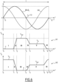
- control device 20 is configured to operate the piezoelectric material of the piezoelectric resonator 15 at its resonance in order to exploit charge transfer phases making it possible to dispense with the use of an inductive element, while regulating the output voltage by maintaining the resonance of the piezoelectric material, that is to say with repeated switching cycles at an operating frequency dependent on the oscillation frequency of the piezoelectric resonator 15, and by adjusting the durations of the respective switching phases within the resonance cycle.
- the oscillation frequency is the frequency at which the resonator 12, such as the piezoelectric resonator 15, oscillates and consequently its current I L on its motional branch (RLC branch) of its equivalent model around the selected resonance mode.
- the current I L can be deduced either by observing the evolution of the voltage V p when the resonator is isolated or by observing its output current I p during the constant voltage phases.
- the conversion cycle is synchronized with a mechanical movement of the piezoelectric resonator 15, and the driving frequency is then set to the mechanical oscillation frequency. In practice, this oscillation frequency depends on the operating point of the converter 10: values of the three voltage steps and the output current.
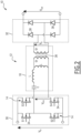
- the switching circuit 30, in its H-bridge form, comprises for example four transistors 34 forming the switches 14, also denoted S1, S2, S3, S4.
- the transistors 34 are for example MOSFET transistors, such as N-type depletion MOSFET transistors.
- the control device 20 is configured to control the electrical energy converter 10, and in particular the switching of the switches 14 of the energy converter.
- control device 20 comprises a measuring module 40, a generation module 42 and a control module 44 for a respective switch 14.
- the measurement module 40, the generation module 42, and the control module 44 are for example each produced in the form of an electronic circuit comprising one or more electronic components, and in particular comparators when comparisons are carried out.
- the measurement module 40, the generation module 42, and the control module 44 are each implemented in the form of a programmable logic component, such as an FPGA (Field Programmable Gate Array), or in the form of an integrated circuit, such as an ASIC (Application Specific Integrated Circuit) or in the form of a computer, such as a microcontroller, a processor.
- the measurement module 40, the generation module 42, and the control module 44 are implemented together within a single hardware component, such as a single programmable logic component, a single integrated circuit, or a single computer.
- the measurement module 40 is configured to measure a regulation quantity G reg .
- the regulation quantity G reg is for example the voltage V p across the terminals of the resonator 12.
- the regulation quantity G reg is another quantity representative of the resonator 12, such as the current I p .
- the control variable is preferably measured just before switching the switch 14.
- the control variable is measured less than 20 ns, preferably less than 2 ns before switching on the respective switch 14.
- the generation module 42 is configured to generate a reference triangular signal 45, for subsequent use in controlling the respective switch 14.
- the reference signal 45 is a periodic triangular voltage V ramp forming a ramp at each resonance cycle of the resonator 12.
- the ramp formed by the triangular voltage V ramp has a ramp period T ramp , the ramp period T ramp being preferably equal to the resonance period, the ramp period T ramp then being equal to the inverse of the oscillation frequency of the resonator 12.
- a time instant of the start of the reference signal period is typically determined as a function of the regulation quantity G reg .
- the time instant of the start of the period of the reference signal preferentially depends on a time instant at which the time derivative of the regulation quantity G reg is zero.
- the regulation quantity G reg is the voltage V p across the terminals of the resonator 12
- the time instant at which the time derivative of the regulation quantity G reg is zero then corresponds to the zero crossing of the current I L flowing in the resonator 12, the time derivative of the voltage V p being an image of said current I L .
- the period start time instant is anticipated with respect to a switching time instant t i of a corresponding switch, a time difference between the period start time instant and the switching time instant t i depending on a processing delay by a control unit 58 of the respective switch 14, described below, i.e. the processing delay from the transmission of a switching command until the switching of the switch 14.
- the ramp is advanced by the delay of the control of the switching of the respective switch 14.
- the ramp is ahead of the switching of the respective switch 14.
- the reference triangular signal 45 has a characteristic quantity G car depending on the oscillation frequency of the resonator 12, the characteristic quantity G car being chosen from the group consisting of: a slope ⁇ of the reference triangular signal 45 and an amplitude A mp of the reference triangular signal 45.
- the control module 44 is configured to control each switch 14 as a function of the reference triangular signal 45, in particular from a comparison with the reference triangular signal 45.
- the generation module 42 comprises a derivation unit 46, a sampling unit 48, a differential unit 50, a corrector 52 and a ramp generator 54.
- the generation module 42 is connected to the output of the measurement module 40, and capable of receiving as input the regulation quantity G reg , such as the voltage V p at the terminals of the resonator 12. In addition, the generation module 42 is capable of receiving a reset command and a value of a sampling instant t sa of the respective switch 14 which is controlled by the control device 20.
- the derivation unit 46 is typically configured to calculate the derivative of an input signal, namely the regulation quantity G reg , such as the voltage V p across the resonator 12, and by calculating its time derivative, to deliver a voltage V der representative of said time derivative.
- G reg the regulation quantity
- the voltage V der is typically an image of the current I L flowing in the resonator 12, being directly proportional to the value of the current I L when the regulation quantity G reg is the voltage V p and the voltage V der then corresponds to dV p /dt and considering that the resonator 12 is in open circuit during sampling.
- the sampling unit 48 is connected to the output of the derivation unit 46 and to the control module 44, and is then able to receive as input the voltage V der and the sampling instant t sa , advantageously less than 20 ns, advantageously substantially 1 ns to 2 ns, before the actual switching of the respective switch 14.
- the sampling unit 48 is typically configured to choose a sampling duration, for example substantially equal to 1% of the total duration of a cycle.
- the sampling time t sa is adjustable via a programmable time delay, for example integrated on the electronic circuit forming the generation module 42, the time reference typically being a rising or falling signal edge upstream or inside the control unit 58 of the respective switch 14.
- the sampling unit 48 is capable of delivering a voltage V sa corresponding to the voltage V der sampled at the sampling instant t sa .
- the differential unit 50 is connected to the output of the sampling unit 48, and is then able to receive as input the voltage V sa and a reference voltage V cons .
- the setpoint voltage V cons advantageously corresponds to the desired setpoint value of the current at the sampling instant t sa , such as the value 0 for the instant t 0 in the example described below with regard to figures 6 And 7 .
- the differential unit 50 is intended to deliver a voltage V sa ' resulting from the difference between the voltages V sa and V cons .
- the differential unit 50 is for example in the form of a subtractor, capable of subtracting the reference voltage V cons from the voltage V sa to deliver the resulting voltage V sa '.
- the corrector 52 is connected to the output of the differential unit 50, and is then able to receive the voltage V sa ' as input.
- the corrector 52 is typically configured to perform a regulation of the periodic switching control instant of the respective switch 14, by receiving as input the voltage V sa ' from the sampling unit 48, by calculating an error ⁇ between this voltage V sa ' and a target voltage, and then performing an integration of this error ⁇ . The corrector 52 is then able to deliver a voltage V M .
- the corrector 52 comprises for example an operational amplifier 52A, a resistor 52B and a feedback loop with a capacitor 52C.
- the feedback loop connects the output of the operational amplifier 52A to its negative input.
- the electrical resistor 52B is connected between the input of the corrector 52 receiving the voltage V sa ' and the negative input of the operational amplifier 52A.
- any other type of corrector can be used, for example proportional-integral or proportional-integral-derivative.
- the ramp generator 54 is connected to the output of the corrector 52, and is configured to generate the triangular voltage V ramp forming a ramp for controlling the respective switch 14, namely a control reference for all the switching times of the switches 14, the characteristic quantity G car , such as the slope ⁇ of the ramp, being adapted as a function of the value of the output voltage V M of the corrector 52.
- the ramp generator 54 is for example intended to adjust the value of the slope ⁇ of the triangular voltage V ramp in order to regulate all switching instants; and to reset the ramp of the triangular voltage V ramp to zero.
- the slope ⁇ is therefore modified according to the oscillation frequency of the resonator 12, while keeping the amplitude Amp of the triangular voltage V ramp constant.
- the ramp generator 54 is intended to adjust the value of the amplitude Amp of the triangular voltage V ramp in order to regulate all switching instants.
- the amplitude Amp is therefore modified as a function of the oscillation frequency of the resonator 12, while keeping the slope ⁇ of the triangular voltage V ramp constant.
- control module 44 comprises a comparator 56 and the control unit 58.
- the control module 44 is connected to the output of the generation module 42, and then able to receive the voltage V ramp as input.
- Comparator 56 is connected to the output of ramp generator 54, and is then able to receive voltage V ramp .
- control modules 44 there are as many control modules 44 as there are switches 14, i.e. half of the desired switching times during the resonance cycle, each switch 14 being switched once to closing and once to opening during the resonance cycle.
- switches 14 i.e. half of the desired switching times during the resonance cycle, each switch 14 being switched once to closing and once to opening during the resonance cycle.
- t i , i being between 0 and 6 in the example described.
- Each switching instant t i is associated with a respective control signal.
- each switching instant t i is associated with a respective control voltage V ti .
- each switch 14 is associated with two switching times t i , and then each switch 14 is associated with two respective control signals.
- Each control voltage V ti is advantageously between a minimum stop V ti_min and a maximum stop V ti_max , the minimum stops V ti_min and maximum V ti_max being predefined by the user and defining minimum values t i_min and maximum values t i_max of the control instants t i .
- the control unit 58 then comprises for example an RS flip-flop, with the S input connected to CompOn and the R input connected to CompOff, the Q output delivering the control signal of the switch in question; or a D flip-flop with Reset, with the D input in the high state, the Clock input connected to CompOn and the R input connected to CompOff, the Q output delivering the control signal of the switch in question; or a logic circuit performing the operation (CompOn and Not(CompOff)), the result forming the control signal of the switch in question.
- the control unit 58 is connected to the input of the respective switch 14, and is configured to apply the opening control signal, or respectively the closing control signal, to a control electrode of the switch 14, such as a gate electrode when the switch 14 comprises a transistor such as a MOSFET or an IGBT.
- the ramp generator 54 comprises an operational amplifier 60, a source follower 62, a current mirror 64 and a generation unit 66.
- the operational amplifier 60 is connected, by its positive input, to the output of the corrector 52, and is then able to receive the voltage V M .
- the negative input of the operational amplifier is connected to the output of the source follower 62.
- the source follower 62 comprises a transistor T1, a transistor T2 and a resistor R0 , the transistor T2 and the resistor R0 being connected in series and forming a resistance equivalent R tot .
- the control electrode of transistor T1 is connected to the output of operational amplifier 60.
- a first conduction electrode of the transistor T1 is connected to the negative terminal of the operational amplifier 60 and to the equivalent resistance R tot , a second conduction electrode of the transistor T1 delivering a current I 1 .
- the operational amplifier 60 is therefore intended to compensate the threshold voltage of the transistor T1, in order to reduce the variation of the current I 1 .
- the control of transistor T2 is for example connected to a high potential, such as a supply voltage V DD , to keep transistor T2 closed.
- the current mirror 64 comprises two transistors T3 and T4, the transistors T3 and T4 being, for example, PMOS type transistors.
- the current mirror 64 is connected to the output of the source follower 62, by its connection with the second conduction electrode of the transistor T1 and therefore receives the current I 1 .
- the current mirror 64 is intended to deliver at the output a current substantially identical to the current I 1 , typically to within 5%, whatever the load applied at the output of the current mirror 64.
- the current I1 is applied to the control electrodes of the transistors T3 and T4 and to a first conduction electrode of T3, second conduction electrodes of the transistors T3 and T4 being electrically connected to each other; and a replicated current I R being obtained at a first conduction electrode of T4.
- the generation unit 66 comprises a branch circuit 67 as well as a pulse module 68.
- the generation unit 66 is connected to the output of the current mirror 64, and is then able to receive the current I R as input.
- Branch circuit 67 is intended to deliver the voltage V ramp .
- the branch circuit 67 comprises 6 electrical branches 70, 72, 74, 76, 78 and 80 in branch, the voltage V ramp being at the terminals of each of the electrical branches 70, 72, 74, 76, 78 and 80.
- the voltage V ramp being at the terminals of each of the electrical branches 70, 72, 74, 76, 78 and 80.
- branch 80 it is possible to use any other number of branch(es) including at least branch 80, the higher the number of branches, the finer the frequency adjustment can be and/or over a wide frequency range.
- the first branch 70 comprises a capacitor C0.
- the value of the capacitor C0 is typically between 0.1 and 10 pF, notably approximately equal to 0.7 pF.
- the second branch 72 comprises a switch P0, the switch P0 being intended to be controlled by the pulsing module 68.
- the third branch 74 comprises a capacitor C1 and a switch P1, the capacitor C1 and the switch P1 being connected in series.
- capacitor C1 is typically between 0.04 and 10 pF, notably approximately equal to 0.4 pF.
- Switch P1 is intended to be controlled by a control bit b 1 predefined by the user, switch P1 being in the open position when bit b 1 is equal to 0 and in the closed position when bit b 1 is equal to 1.
- the fourth branch 76 comprises a capacitor C2 and a switch P2, the capacitor C2 and the switch P2 being connected in series.
- capacitor C2 is typically between 0.4 and 50 pF, notably approximately equal to 4 pF.
- Switch P2 is intended to be controlled by a control bit b 2 predefined by the user, switch P2 being in the open position when bit b 2 is equal to 0 and in the closed position when bit b 2 is equal to 1.
- the fifth branch 78 comprises a capacitor C3 and a switch P3, the capacitor C3 and the switch P3 being connected in series.
- capacitor C3 is typically between 1 and 150 pF, notably approximately equal to 12 pF.
- Switch P3 is intended to be controlled by a user-defined control bit b3 , with switch P3 being in the open position when bit b3 is 0 and in the closed position when bit b3 is 1.
- the sixth branch 80 comprises a switch P4, the switch P4 being intended to be controlled by the pulsing module 68.
- this capacitive configuration is used to preset a central frequency. Regulation via the voltage V M , also called the end of ramp voltage, then makes it possible to adjust the frequency around this central frequency. This is a presetting either in advance or at the start of the converter 10 to place itself on a frequency band consistent with the piezoelectric resonator 15 on the chosen resonance mode.
- the pulsation module 68 is connected to the output of the comparator 56 associated with the regulation of the duration of the resonance cycle, that is to say the regulation of the resonance period, and is then able to receive a voltage V reset as input.
- the V reset voltage is a square wave voltage, presenting a high logic level if the V ramp voltage exceeds the end of ramp voltage V M , and a low logic level otherwise.
- the pulse module 68 is intended to discharge the capacitors C0, C1, C2 and C3 when the voltage V reset has a high logic level, indicating that the ramp has enabled the switching of all switching instants and that it must therefore be reset.
- the pulsation module 68 is intended to control the switches P0 and/or P4 in their closed position, in order to discharge the capacitors C0, C1, C2 and C3; when the threshold voltage V M allowing the control of the last switching instant is desired.
- the pulsation module 68 is capable of delivering a voltage V pulse whose time width is predefined and makes it possible to choose a discharge duration D of the capacitors C0, C1, C2 and C3.
- the discharge time D of capacitors is typically less than 10ns, for example chosen between 2ns, 5ns and 10ns.
- the switch P0 is directly controlled by the voltage V pulse .
- Switch P4 is controlled via an AND logic gate 82.
- the AND logic gate 82 is connected to the output of the pulse module 68 and an OR logic gate 84, and then able to receive the voltage V pulse and a voltage V OR as input.
- the AND logic gate 82 is capable of delivering a voltage V AND as output, the voltage V AND typically also being in the form of a square wave voltage with a high logic level if the voltages V pulse and V OR have a high logic level, and with a low logic level otherwise.
- the switch P4 is controlled in the closed position if V AND has a high logic level, or is controlled in the open position if V AND has a low logic level.
- the OR logic gate 84 is capable of receiving as input the bit b 2 and the bit b 3 , previously defined by the user.
- the OR logic gate 84 is capable of delivering the voltage V OR as output, the voltage V OR being typically in the form of a square wave voltage with a high logic level if b 2 and/or b 3 have(s) a value equal to 1, and with a low logic level otherwise.
- switch P4 is placed closest to capacitors C2 and C3, because capacitors C2 and C3 have typically larger capacitances than capacitors C0 and C1 and require more time to discharge. Switch P4 is therefore only activated when capacitor C3 or C4 or both are used for ramp signal generation.
- f ramp V M C ramp . ⁇ V ramp . R tot where the parameters are identical to those of the previous equation [2].
- a first phase I begins at substantially constant voltage, at the zero value according to the first mode M1 via the closing of the second switch K2, or at the input voltage V in according to the second mode M2 via the closing of the first switch K1, and lasts until a time instant t 1 which forms an adjustment parameter of the converter 10, this time instant t 1 making it possible to define the voltage, the current or even the desired power at the output of the converter 10.
- the time instant t 1 then corresponds to the end of the first phase I and to the instant at which the second switch K2 according to the first mode M1, or respectively the first switch K1 according to the second mode M2, must then be open, the instant time t 1 forming a second switching time instant corresponding to the opening of the second switch K2 according to the first mode M1, or respectively of the first switch K1 according to the second mode M2.
- a second phase II begins, corresponding to a phase with substantially constant load, or else in a substantially open circuit, this second phase II lasting until a time instant t 2 defined by the transition to a new predefined value of the voltage V p at the terminals of the piezoelectric resonator 15.
- the time instant t 2 forming the end of the second phase II typically corresponds to the closing of the third switch K3 according to the first mode M1, or respectively of the second switch K2 according to the second mode M2, the time instant t 2 then forming a third switching time instant.
- this fourth phase IV corresponds to a phase with substantially constant charge, this fourth phase flowing between the time instant t 3 and the time instant t 4 .
- the end of this fourth phase VI corresponds to the moment when the voltage V p at the terminals of the piezoelectric resonator 15 reaches the input voltage V in according to the first mode M1, or the output voltage V out according to the second mode M2.
- a fifth switching time instant corresponds to the closing of the first switch K1 for the first mode M1, respectively of the third switch K3 for the second mode M2, and the voltage V p across the terminals of the piezoelectric resonator 15 is then substantially constant and equal to the input voltage V in according to the first mode M1, or to the output voltage V out according to the second mode M2.
- t 4 begins a fifth phase V lasting until the opening of the switch which was closed at the fifth switching time instant t 4 .
- a sixth switching time instant, noted t 5 corresponds to the opening of the first switch K1 for the first mode M1, respectively of the third switch K3 for the second mode M2, and the voltage V p across the terminals of the piezoelectric resonator 15 then goes from a previous voltage V in according to the first mode M1, or V out according to the second mode M2, to an open circuit position.
- At this sixth switching time instant t 5 then begins a sixth phase VI lasting until a time instant t 6 corresponding to a zero crossing of the current I L flowing in the piezoelectric resonator 15.
- the time instant t 5 has been defined so that at the time instant t 6 , the voltage V p at the terminals of the piezoelectric resonator 15 reaches a value corresponding to the value allowing zero voltage switching of the corresponding switch.
- time instant t 6 is equal to the sum of the time instant t 0 and the period T of the resonance cycle, and is also denoted (t 0 +T).
- the time instant t 6 corresponds to the end of a resonance cycle of the piezoelectric resonator 15.
- the measuring module 40 measures the regulation quantity G reg of the converter 10.
- the regulation quantity G reg is advantageously the voltage V p across the terminals of the resonator 12.
- the generation module 42 In a second step 110, the generation module 42 generates the reference triangular signal 45, then synchronizes it with the regulation quantity G reg measured by the measurement module 40, the regulation quantity G reg depending on the oscillation frequency of the resonator 12.
- the generation module 42 synchronizes the reference triangular signal 45 with the regulation quantity G reg at least once per resonance cycle, in particular once per resonance cycle.
- control module 44 receives the reference triangular signal 45 from the generation module 42, in particular via the ramp generator 54, and controls a switching of each of the switches 14, according to several successive phases during a resonance cycle of the resonator 12, each phase resulting from a switching of at least one respective switch.
- the switching times of the different switches 14 are determined by comparison with the reference triangular signal 45.
- each switching instant t 0 , t 1 , t 2 , t 3 , t 4 , t 5 or t 6 is connected to a respective control signal, here a respective control voltage V t0 , V t1 , V t2 , V t3 , V t4 , V t5 or V t6 .
- the switch associated with each instant t 0 , t 1 , t 2 , t 3 , t 4 , t 5 or t 6 is then switched when the voltage V ramp corresponding to the reference signal reaches the control voltage respective V t0 , V t1 , V t2 , V t3 , V t4 , V t5 , V t6 , or the respective minimum stop V t0_min , V t1_min , V t2_min , V t3_min , V t4_min , V t5_min , V t6_min when the respective control voltage V ti is lower than said respective minimum stop V ti_min ; or the respective maximum stop V t0_max , V ti_max , V t2_max , V t3_max , V t4_max , V t5_max , V t6_max when the respective control voltage V ti is higher
- the high precision of the switching instants makes it possible to minimize switching losses and maintain smooth switching conditions, in particular at zero voltage or ZVS (from the English Zero Voltage Switching ) , which allows the converter 10 to operate optimally at high frequencies.
Landscapes
- Engineering & Computer Science (AREA)
- Power Engineering (AREA)
- Dc-Dc Converters (AREA)
Applications Claiming Priority (1)
| Application Number | Priority Date | Filing Date | Title |
|---|---|---|---|
| FR2314516A FR3157030A1 (fr) | 2023-12-19 | 2023-12-19 | Dispositif électronique et procédé de pilotage, avec commande via signal triangulaire synchronisé, d’un convertisseur d’énergie électrique comportant un résonateur, système de conversion d’énergie électrique associé |
Publications (1)
| Publication Number | Publication Date |
|---|---|
| EP4576531A1 true EP4576531A1 (de) | 2025-06-25 |
Family
ID=90904499
Family Applications (1)
| Application Number | Title | Priority Date | Filing Date |
|---|---|---|---|
| EP24221235.5A Pending EP4576531A1 (de) | 2023-12-19 | 2024-12-18 | Elektronische vorrichtung und verfahren zur steuerung eines elektrischen energiewandlers mit synchronisiertem dreiecksignal und stromwandlersystem dafür |
Country Status (3)
| Country | Link |
|---|---|
| US (1) | US20250202369A1 (de) |
| EP (1) | EP4576531A1 (de) |
| FR (1) | FR3157030A1 (de) |
Citations (3)
| Publication number | Priority date | Publication date | Assignee | Title |
|---|---|---|---|---|
| US20150084607A1 (en) * | 2013-09-20 | 2015-03-26 | Fujitsu Limited | Power supply apparatus |
| EP3627688A1 (de) * | 2018-09-21 | 2020-03-25 | Commissariat à l'Energie Atomique et aux Energies Alternatives | Leistungswandler |
| FR3086471A1 (fr) | 2018-09-21 | 2020-03-27 | Commissariat A L'energie Atomique Et Aux Energies Alternatives | Convertisseur de puissance |
-
2023
- 2023-12-19 FR FR2314516A patent/FR3157030A1/fr active Pending
-
2024
- 2024-12-18 US US18/985,803 patent/US20250202369A1/en active Pending
- 2024-12-18 EP EP24221235.5A patent/EP4576531A1/de active Pending
Patent Citations (4)
| Publication number | Priority date | Publication date | Assignee | Title |
|---|---|---|---|---|
| US20150084607A1 (en) * | 2013-09-20 | 2015-03-26 | Fujitsu Limited | Power supply apparatus |
| EP3627688A1 (de) * | 2018-09-21 | 2020-03-25 | Commissariat à l'Energie Atomique et aux Energies Alternatives | Leistungswandler |
| FR3086471A1 (fr) | 2018-09-21 | 2020-03-27 | Commissariat A L'energie Atomique Et Aux Energies Alternatives | Convertisseur de puissance |
| FR3086472A1 (fr) | 2018-09-21 | 2020-03-27 | Commissariat A L'energie Atomique Et Aux Energies Alternatives | Convertisseur de puissance |
Non-Patent Citations (5)
| Title |
|---|
| B. POLLETG. DESPESSEF. COSTA: "A New Non-Isolated Low-Power Inductorless Piezoelectric DC-DC Converter", IEEE TRANSACTIONS ON POWER ELECTRONICS, vol. 34, no. 11, XP011744096, DOI: 10.1109/TPEL.2019.2900526 |
| FORRESTER JACK ET AL: "Resonant current estimation and phase-locked loop control system for inductorless step-up single piezo element-based (SUPRC) DC-DC converter", IECON 2022 - 48TH ANNUAL CONFERENCE OF THE IEEE INDUSTRIAL ELECTRONICS SOCIETY, IEEE, 17 October 2022 (2022-10-17), pages 1 - 6, XP034243772, DOI: 10.1109/IECON49645.2022.9969043 * |
| J. J. PIELJ. D. BOLESJ. H. LANGD. J. PERREAULT: "eedback Control for a Piezoelectric-Resonator-Based DC-DC Power Converter", IEEE 22ND WORKSHOP ON CONTROL AND MODELLING OF POWER ELECTRONICS (COMPEL, 2021 |
| M. TOUHAMIG. DESPESSEF. COSTAB. POLLET: "Implementation of Control Strategy for Step-down DC-DC Converter Based on Piezoelectric Resonato", 22ND EUROPEAN CONFERENCE ON POWER ELECTRONICS AND APPLICATIONS (EPE'20 ECCE EUROPE, 2020 |
| P. A. KYAWC. R. SULLIVAN: "Fundamental examination of multiple potential passive component technologies for future power electronics", IEEE 16TH WORKSHOP ON CONTROL AND MODELING FOR POWER ELECTRONICS (COMPEL, 2015 |
Also Published As
| Publication number | Publication date |
|---|---|
| US20250202369A1 (en) | 2025-06-19 |
| FR3157030A1 (fr) | 2025-06-20 |
Similar Documents
| Publication | Publication Date | Title |
|---|---|---|
| EP3627688B1 (de) | Leistungswandler | |
| EP4191854B1 (de) | Elektronische vorrichtung und verfahren zur gleichtaktfreien steuerung eines elektrischen energiewandlers mit zwei piezoelektrischen elementen, elektronisches stromwandlersystem dafür | |
| EP3627687A1 (de) | Leistungswandler | |
| EP3910775A1 (de) | Steuerung eines stromwandlers mit partitionierung | |
| EP3910774A1 (de) | Steuerung eines stromwandlers mit partitionierung | |
| WO2017064220A1 (fr) | Convertisseur dc/dc isole | |
| EP4068606B1 (de) | Spannungswandler | |
| EP4576531A1 (de) | Elektronische vorrichtung und verfahren zur steuerung eines elektrischen energiewandlers mit synchronisiertem dreiecksignal und stromwandlersystem dafür | |
| EP3843255B1 (de) | Schaltung zur steuerung der eingangsimpedanz einer rekuperator-schnittstelle | |
| EP4117161B1 (de) | Steuerung und steuerungsverfahren mit zusätzlichem freiheitsgrad für einen piezoelektrischen energiewandler | |
| EP1564876B1 (de) | Schweisseinrichtung mit sanfschaltendem Quasi-resonanzwechselrichter | |
| EP4080747A1 (de) | Elektronische vorrichtung und verfahren zur steuerung eines elektrischen energiewandlers mit einem piezoelektrischen element und entsprechendes elektronisches system zur umwandlung von elektrischer energie | |
| EP4576530A1 (de) | Elektronische vorrichtung und verfahren zur steuerung eines elektrischen energiewandlers mit resonator, zugehöriges stromwandlersystem | |
| WO2018220284A1 (fr) | Procédé d'optimisation de la durée d'un temps mort lors des commutations d'un bras d'interrupteur commande en fréquence | |
| EP4576532A1 (de) | Elektronische vorrichtung und verfahren zur ansteuerung mit unterdrückung mindestens einer energieerzeugenden phase eines elektrischen energiewandlers mit einem piezoelektrischen resonator, zugehöriges stromwandlersystem | |
| EP4191852B1 (de) | Stromwandler mit piezoelektrischem element und schalthilfsschaltung(en), elektronisches stromwandlersystem | |
| FR3131133A1 (fr) | Système de conversion d’énergie électrique avec ensemble(s) piézoélectrique(s) et transformateur électrique | |
| EP4191853B1 (de) | Elektrischer energiewandler mit mindestens einem paar piezoelektrischer anordnungen und mindestens einem komplementären direktverbindungsschalter, umwandlungssystem und steuerungsverfahren dafür | |
| EP1420466A2 (de) | Elektronische Steuervorrichtung für einen piezoelektrischen Ultraschallaktuator | |
| EP3910776A1 (de) | Steuerung eines stromwandlers mit partitionierung | |
| FR3161081A1 (fr) | Dispositif électronique et procédé de pilotage d’un convertisseur d’énergie électrique, système électronique de conversion d’énergie électrique associé | |
| WO2020016140A1 (fr) | Procede de gestion des commutations d'un bras d'interrupteur commande en frequence | |
| EP4447302A1 (de) | Doppelbrücken-schaltwandlersteuerung | |
| FR2793598A1 (fr) | Dispositif electronique permettant l'alimentation et le controle d'actionneurs piezoelectriques | |
| WO2025141122A1 (fr) | Dispositif électronique et procédé de pilotage d'un convertisseur d'énergie électrique comportant des élément(s) piézoélectrique(s), système électronique de conversion d'énergie électrique associé |
Legal Events
| Date | Code | Title | Description |
|---|---|---|---|
| PUAI | Public reference made under article 153(3) epc to a published international application that has entered the european phase |
Free format text: ORIGINAL CODE: 0009012 |
|
| STAA | Information on the status of an ep patent application or granted ep patent |
Free format text: STATUS: REQUEST FOR EXAMINATION WAS MADE |
|
| 17P | Request for examination filed |
Effective date: 20241218 |
|
| AK | Designated contracting states |
Kind code of ref document: A1 Designated state(s): AL AT BE BG CH CY CZ DE DK EE ES FI FR GB GR HR HU IE IS IT LI LT LU LV MC ME MK MT NL NO PL PT RO RS SE SI SK SM TR |