EP4576223A1 - Reverse conducting igbt power device and preparation method therefor, and electronic device - Google Patents
Reverse conducting igbt power device and preparation method therefor, and electronic device Download PDFInfo
- Publication number
- EP4576223A1 EP4576223A1 EP23854091.8A EP23854091A EP4576223A1 EP 4576223 A1 EP4576223 A1 EP 4576223A1 EP 23854091 A EP23854091 A EP 23854091A EP 4576223 A1 EP4576223 A1 EP 4576223A1
- Authority
- EP
- European Patent Office
- Prior art keywords
- collector
- layer
- power device
- reverse conducting
- conductivity type
- Prior art date
- Legal status (The legal status is an assumption and is not a legal conclusion. Google has not performed a legal analysis and makes no representation as to the accuracy of the status listed.)
- Pending
Links
Images




Classifications
-
- H—ELECTRICITY
- H10—SEMICONDUCTOR DEVICES; ELECTRIC SOLID-STATE DEVICES NOT OTHERWISE PROVIDED FOR
- H10D—INORGANIC ELECTRIC SEMICONDUCTOR DEVICES
- H10D12/00—Bipolar devices controlled by the field effect, e.g. insulated-gate bipolar transistors [IGBT]
- H10D12/411—Insulated-gate bipolar transistors [IGBT]
- H10D12/441—Vertical IGBTs
- H10D12/461—Vertical IGBTs having non-planar surfaces, e.g. having trenches, recesses or pillars in the surfaces of the emitter, base or collector regions
- H10D12/481—Vertical IGBTs having non-planar surfaces, e.g. having trenches, recesses or pillars in the surfaces of the emitter, base or collector regions having gate structures on slanted surfaces, on vertical surfaces, or in grooves, e.g. trench gate IGBTs
-
- H—ELECTRICITY
- H10—SEMICONDUCTOR DEVICES; ELECTRIC SOLID-STATE DEVICES NOT OTHERWISE PROVIDED FOR
- H10D—INORGANIC ELECTRIC SEMICONDUCTOR DEVICES
- H10D10/00—Bipolar junction transistors [BJT]
- H10D10/01—Manufacture or treatment
-
- H—ELECTRICITY
- H10—SEMICONDUCTOR DEVICES; ELECTRIC SOLID-STATE DEVICES NOT OTHERWISE PROVIDED FOR
- H10D—INORGANIC ELECTRIC SEMICONDUCTOR DEVICES
- H10D12/00—Bipolar devices controlled by the field effect, e.g. insulated-gate bipolar transistors [IGBT]
- H10D12/01—Manufacture or treatment
-
- H—ELECTRICITY
- H10—SEMICONDUCTOR DEVICES; ELECTRIC SOLID-STATE DEVICES NOT OTHERWISE PROVIDED FOR
- H10D—INORGANIC ELECTRIC SEMICONDUCTOR DEVICES
- H10D12/00—Bipolar devices controlled by the field effect, e.g. insulated-gate bipolar transistors [IGBT]
- H10D12/01—Manufacture or treatment
- H10D12/031—Manufacture or treatment of IGBTs
- H10D12/032—Manufacture or treatment of IGBTs of vertical IGBTs
- H10D12/038—Manufacture or treatment of IGBTs of vertical IGBTs having a recessed gate, e.g. trench-gate IGBTs
-
- H—ELECTRICITY
- H10—SEMICONDUCTOR DEVICES; ELECTRIC SOLID-STATE DEVICES NOT OTHERWISE PROVIDED FOR
- H10D—INORGANIC ELECTRIC SEMICONDUCTOR DEVICES
- H10D12/00—Bipolar devices controlled by the field effect, e.g. insulated-gate bipolar transistors [IGBT]
- H10D12/411—Insulated-gate bipolar transistors [IGBT]
-
- H—ELECTRICITY
- H10—SEMICONDUCTOR DEVICES; ELECTRIC SOLID-STATE DEVICES NOT OTHERWISE PROVIDED FOR
- H10D—INORGANIC ELECTRIC SEMICONDUCTOR DEVICES
- H10D12/00—Bipolar devices controlled by the field effect, e.g. insulated-gate bipolar transistors [IGBT]
- H10D12/411—Insulated-gate bipolar transistors [IGBT]
- H10D12/417—Insulated-gate bipolar transistors [IGBT] having a drift region having a doping concentration that is higher at the collector side relative to other parts of the drift region
-
- H—ELECTRICITY
- H10—SEMICONDUCTOR DEVICES; ELECTRIC SOLID-STATE DEVICES NOT OTHERWISE PROVIDED FOR
- H10D—INORGANIC ELECTRIC SEMICONDUCTOR DEVICES
- H10D62/00—Semiconductor bodies, or regions thereof, of devices having potential barriers
- H10D62/10—Shapes, relative sizes or dispositions of the regions of the semiconductor bodies; Shapes of the semiconductor bodies
- H10D62/124—Shapes, relative sizes or dispositions of the regions of semiconductor bodies or of junctions between the regions
- H10D62/126—Top-view geometrical layouts of the regions or the junctions
- H10D62/127—Top-view geometrical layouts of the regions or the junctions of cellular field-effect devices, e.g. multicellular DMOS transistors or IGBTs
-
- H—ELECTRICITY
- H10—SEMICONDUCTOR DEVICES; ELECTRIC SOLID-STATE DEVICES NOT OTHERWISE PROVIDED FOR
- H10D—INORGANIC ELECTRIC SEMICONDUCTOR DEVICES
- H10D62/00—Semiconductor bodies, or regions thereof, of devices having potential barriers
- H10D62/10—Shapes, relative sizes or dispositions of the regions of the semiconductor bodies; Shapes of the semiconductor bodies
- H10D62/13—Semiconductor regions connected to electrodes carrying current to be rectified, amplified or switched, e.g. source or drain regions
- H10D62/137—Collector regions of BJTs
-
- H—ELECTRICITY
- H10—SEMICONDUCTOR DEVICES; ELECTRIC SOLID-STATE DEVICES NOT OTHERWISE PROVIDED FOR
- H10D—INORGANIC ELECTRIC SEMICONDUCTOR DEVICES
- H10D62/00—Semiconductor bodies, or regions thereof, of devices having potential barriers
- H10D62/10—Shapes, relative sizes or dispositions of the regions of the semiconductor bodies; Shapes of the semiconductor bodies
- H10D62/13—Semiconductor regions connected to electrodes carrying current to be rectified, amplified or switched, e.g. source or drain regions
- H10D62/141—Anode or cathode regions of thyristors; Collector or emitter regions of gated bipolar-mode devices, e.g. of IGBTs
- H10D62/142—Anode regions of thyristors or collector regions of gated bipolar-mode devices
-
- H—ELECTRICITY
- H10—SEMICONDUCTOR DEVICES; ELECTRIC SOLID-STATE DEVICES NOT OTHERWISE PROVIDED FOR
- H10D—INORGANIC ELECTRIC SEMICONDUCTOR DEVICES
- H10D62/00—Semiconductor bodies, or regions thereof, of devices having potential barriers
- H10D62/10—Shapes, relative sizes or dispositions of the regions of the semiconductor bodies; Shapes of the semiconductor bodies
- H10D62/17—Semiconductor regions connected to electrodes not carrying current to be rectified, amplified or switched, e.g. channel regions
- H10D62/393—Body regions of DMOS transistors or IGBTs
-
- H—ELECTRICITY
- H10—SEMICONDUCTOR DEVICES; ELECTRIC SOLID-STATE DEVICES NOT OTHERWISE PROVIDED FOR
- H10D—INORGANIC ELECTRIC SEMICONDUCTOR DEVICES
- H10D64/00—Electrodes of devices having potential barriers
- H10D64/20—Electrodes characterised by their shapes, relative sizes or dispositions
- H10D64/23—Electrodes carrying the current to be rectified, amplified, oscillated or switched, e.g. sources, drains, anodes or cathodes
- H10D64/231—Emitter or collector electrodes for bipolar transistors
-
- H—ELECTRICITY
- H10—SEMICONDUCTOR DEVICES; ELECTRIC SOLID-STATE DEVICES NOT OTHERWISE PROVIDED FOR
- H10D—INORGANIC ELECTRIC SEMICONDUCTOR DEVICES
- H10D84/00—Integrated devices formed in or on semiconductor substrates that comprise only semiconducting layers, e.g. on Si wafers or on GaAs-on-Si wafers
- H10D84/01—Manufacture or treatment
- H10D84/0107—Integrating at least one component covered by H10D12/00 or H10D30/00 with at least one component covered by H10D8/00, H10D10/00 or H10D18/00, e.g. integrating IGFETs with BJTs
- H10D84/0109—Integrating at least one component covered by H10D12/00 or H10D30/00 with at least one component covered by H10D8/00, H10D10/00 or H10D18/00, e.g. integrating IGFETs with BJTs the at least one component covered by H10D12/00 or H10D30/00 being a MOS device
-
- H—ELECTRICITY
- H10—SEMICONDUCTOR DEVICES; ELECTRIC SOLID-STATE DEVICES NOT OTHERWISE PROVIDED FOR
- H10D—INORGANIC ELECTRIC SEMICONDUCTOR DEVICES
- H10D84/00—Integrated devices formed in or on semiconductor substrates that comprise only semiconducting layers, e.g. on Si wafers or on GaAs-on-Si wafers
- H10D84/101—Integrated devices comprising main components and built-in components, e.g. IGBT having built-in freewheel diode
- H10D84/161—IGBT having built-in components
-
- H—ELECTRICITY
- H10—SEMICONDUCTOR DEVICES; ELECTRIC SOLID-STATE DEVICES NOT OTHERWISE PROVIDED FOR
- H10D—INORGANIC ELECTRIC SEMICONDUCTOR DEVICES
- H10D84/00—Integrated devices formed in or on semiconductor substrates that comprise only semiconducting layers, e.g. on Si wafers or on GaAs-on-Si wafers
- H10D84/80—Integrated devices formed in or on semiconductor substrates that comprise only semiconducting layers, e.g. on Si wafers or on GaAs-on-Si wafers characterised by the integration of at least one component covered by groups H10D12/00 or H10D30/00, e.g. integration of IGFETs
- H10D84/811—Combinations of field-effect devices and one or more diodes, capacitors or resistors
-
- H—ELECTRICITY
- H10—SEMICONDUCTOR DEVICES; ELECTRIC SOLID-STATE DEVICES NOT OTHERWISE PROVIDED FOR
- H10D—INORGANIC ELECTRIC SEMICONDUCTOR DEVICES
- H10D12/00—Bipolar devices controlled by the field effect, e.g. insulated-gate bipolar transistors [IGBT]
-
- H—ELECTRICITY
- H10—SEMICONDUCTOR DEVICES; ELECTRIC SOLID-STATE DEVICES NOT OTHERWISE PROVIDED FOR
- H10D—INORGANIC ELECTRIC SEMICONDUCTOR DEVICES
- H10D12/00—Bipolar devices controlled by the field effect, e.g. insulated-gate bipolar transistors [IGBT]
- H10D12/01—Manufacture or treatment
- H10D12/031—Manufacture or treatment of IGBTs
- H10D12/032—Manufacture or treatment of IGBTs of vertical IGBTs
- H10D12/035—Etching a recess in the emitter region
-
- H—ELECTRICITY
- H10—SEMICONDUCTOR DEVICES; ELECTRIC SOLID-STATE DEVICES NOT OTHERWISE PROVIDED FOR
- H10D—INORGANIC ELECTRIC SEMICONDUCTOR DEVICES
- H10D64/00—Electrodes of devices having potential barriers
- H10D64/20—Electrodes characterised by their shapes, relative sizes or dispositions
- H10D64/23—Electrodes carrying the current to be rectified, amplified, oscillated or switched, e.g. sources, drains, anodes or cathodes
- H10D64/232—Emitter electrodes for IGBTs
-
- H—ELECTRICITY
- H10—SEMICONDUCTOR DEVICES; ELECTRIC SOLID-STATE DEVICES NOT OTHERWISE PROVIDED FOR
- H10D—INORGANIC ELECTRIC SEMICONDUCTOR DEVICES
- H10D8/00—Diodes
Definitions
- the present disclosure relates to the field of semiconductor device technologies, and in particular, to a reverse conducting IGBT power device, a method for preparing the reverse conducting IGBT power device, and an electronic device having the reverse conducting IGBT power device.
- an additional freewheeling diode is usually required to ensure safety and stability of the system.
- the additional FWD increases the quantity of devices and requires packaging.
- the additional packaging increases the quantity of solder joints, thereby increasing production costs and affecting reliability of the devices.
- the negative differential resistance effect is overcome by increasing the width of the P+ current collector region on the back side, and in some structures, a trench structure and a floating stop ring are arranged on the back side to reduce the voltage snapback phenomenon, thereby suppressing the negative differential resistance effect.
- a trench structure and a floating stop ring are arranged on the back side to reduce the voltage snapback phenomenon, thereby suppressing the negative differential resistance effect.
- other performance of the reverse conducting IGBT device is degraded. Therefore, to overcome the negative differential resistance phenomenon, the structure of the reverse conducting IGBT power device needs to be further improved.
- the present disclosure is intended to resolve at least one of the technical problems in the related art to some extent.
- an embodiment of a first aspect of the present disclosure provides a reverse conducting IGBT power device, which can suppress a negative differential resistance effect.
- An embodiment of a second aspect of the present disclosure further provides a method for preparing a reverse conducting IGBT power device.
- An embodiment of a third aspect of the present disclosure further provides an electronic device having a reverse conducting IGBT power device.
- the reverse conducting IGBT power device provided in this embodiment of the first aspect of the present disclosure includes at least one cell.
- the cell includes:
- a front structure is formed on a front side of the electric field region, and a collector structure is arranged on a back side of the electric field region.
- the collector structure includes a first collector layer of the first conductivity type, a second collector layer of a second conductivity type, a collector insertion layer, a collector interconnection portion, and a collector.
- the second collector layer and the first collector layer are located on a lower surface of the electric field region, the second collector layer is in contact with the first collector layer, both the second collector layer and the first collector layer are connected to the collector, the collector insertion layer is located in the electric field region, and the collector insertion layer is connected to the second collector layer by the collector interconnection portion.
- the collector insertion layer is arranged in the electric field region, and the collector insertion layer is connected to the second collector layer by the collector interconnection portion, so that a length of the second collector layer in a transverse direction of the reverse conducting IGBT power device is increased.
- the reverse conducting IGBT power device is conducted forward, a path for collecting electrons by the collector is extended, and a potential difference can be increased faster to meet a requirement for junction conduction between the second collector layer and the electric field region.
- a PN junction is conducted forward faster, and a voltage snapback is reduced, thereby suppressing a negative differential resistance effect. Other performance of the device is not degraded by the structure either.
- the method for preparing a reverse conducting IGBT power device includes: A substrate is provided, where the substrate has an electric field region.
- a front structure is prepared through photolithography, oxidation, ion injection, and deposition on a front side of the electric field region.
- a first collector layer of a first conductivity type and a second collector layer of a second conductivity type are prepared through photolithography, ion injection, or epitaxy on a back side of the electric field region, and a collector insertion layer and a collector interconnection portion that are of the second conductivity type are prepared in the electric field region, where the collector insertion layer is electrically connected to the second collector layer by the collector interconnection portion.
- a metal electrode is prepared on lower surfaces of the first collector layer and the second collector layer to form a collector.
- the collector insertion layer is prepared in the electric field region, and the collector insertion layer is electrically connected to the second collector layer by the collector interconnection portion, so that a length of the second collector layer in a transverse direction of the reverse conducting IGBT power device is increased.
- the reverse conducting IGBT power device is conducted forward, a path for collecting electrons by the collector is extended, and a potential difference can be increased faster to meet a requirement for junction conduction between the second collector layer and the electric field region.
- APN junction is conducted forward faster, and a voltage snapback is reduced, thereby suppressing a negative differential resistance effect. Other performance of the power device is not degraded.
- the electronic device provided in this embodiment of the third aspect of the present disclosure includes at least one reverse conducting IGBT power device according to any embodiment of the first aspect of the present disclosure.
- the reverse conducting IGBT power device in this embodiment of the present disclosure includes at least one cell.
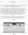
- FIG. 2 is a schematic diagram of a structure of a cell of a reverse conducting IGBT power device according to an embodiment of the present disclosure.
- a cell of the reverse conducting IGBT power device 100 includes an electric field region 101 of a first conductivity type.
- a front structure is formed on a front side 1011 of the electric field region 101.
- the front structure may include an emitter 7, an emitter region 6, an active region 2, and a gate structure (3 and 4).
- the emitter 7 is in ohmic contact with both the emitter region 6 and the active region 2, and the gate structure (3 and 4) is insulated from the emitter 7, the emitter region 6, the active region 2, and the electric field region 101 (for example, insulated by a dielectric layer 5).
- a collector structure is arranged on a back side of the electric field region 101.
- the electric field region 101 may be a drift region 1.
- the electric field region 101 includes a drift region 1 and a field-stop layer 8 (or referred to as a buffer layer), and the field-stop layer 8 is in contact with a lower surface of the drift region 1.
- the reverse conducting IGBT power device 100 in this embodiment of the present disclosure may be of a punch-through structure or a non-punch-through structure.
- the electric field region may be of a non-punch-through (NPT) structure, a punch-through (PT) structure, a soft punch-through (SPT) structure, or a field-stop (FS) structure, which is not specifically limited.
- the gate structure may be a trench gate structure, as shown in FIG. 2 .
- the trench gate structure includes a gate groove of the drift region 1.
- a polysilicon gate 4 and a gate oxide layer 3 are arranged in the gate groove, and the polysilicon gate 4 is insulated from other structures by the dielectric layer 5.
- a dielectric material of the dielectric layer 5 may be a high-k dielectric material such as SiO 2 , HfO 2 , Al 2 O 3 , or Si 3 N 4 .
- the gate structure may alternatively be a planar gate structure, which is not specifically limited herein.
- a collector structure of the reverse conducting IGBT power device 100 in this embodiment of the present disclosure includes a first collector layer 10 of a first conductivity type, a second collector layer 9-2 of a second conductivity type, a collector insertion layer 9-1 (only one layer is shown in FIG. 2 as an example), a collector interconnection portion 9-3, and a collector (not shown).
- the second collector layer 9-2 and the first collector layer 10 are located on a lower surface of the electric field region 101, for example, a lower surface of the drift region or the field-stop region.
- the second collector layer 9-2 is in contact with the first collector layer 10. Both the second collector layer 9-2 and the first collector layer 10 are connected to the collector.
- the collector insertion layer 9-1 is located in the electric field region 101, for example, in the drift region 1 or the field-stop layer 8.
- the collector insertion layer 9-1 is connected to the second collector layer 9-2 by the collector interconnection portion 9-3, that is, the collector is connected.
- the electric field region 101 is a drift region 1, and the collector insertion layer 9-1 is arranged in the drift region 1; and for the non-punch-through structure, the electric field region 101 includes the drift region 1 and the field-stop layer 8 (or referred to as a buffer layer), and the collector insertion layer 9-1 is arranged in the field-stop layer 8, as shown in FIG. 2 .
- the first conductivity type may be N-type, and the second conductivity type is P-type; or the first conductivity type may be P-type, and the second conductivity type is N-type.
- the collector structure in this embodiment of the present disclosure is applicable to an N-channel reverse conducting IGBT power device, and is also applicable to a P-channel reverse conducting IGBT power device.
- an N-channel reverse conducting IGBT power device is used as an example in the embodiments of the present disclosure
- the first conductivity type is N-type
- the second conductivity type is P-type.
- the electric field region 101 includes an N-drift region 1 and an N-type field-stop layer 8.
- the collector structure includes an N+ first collector layer 10 and a P+ collector layer.
- the P+ collector layer may be a double-layer or multi-layer interconnection structure.
- the P+ collector layer includes a P+ collector insertion layer 9-1.
- an electron path passes from the drift region 1 to the field-stop layer 8, and then reaches the first collector such as the N+ first collector layer 10 by transversely bypassing the collector insertion layer 9-1, which is equivalent to prolonging a path for collecting electrons by the collector.
- a potential difference can be increased faster to meet a requirement for junction conduction between the second collector layer 9-2 and the electric field region such as the drift region 1 or the field-stop layer 8, and switching to an IGBT mode faster can be made, thereby reducing a voltage snapback, and suppressing a negative differential resistance effect.
- the collector insertion layer 9-1 is arranged in the electric field region, and the collector insertion layer 9-1 is connected to the second collector layer 9-2 by the collector interconnection portion 9-3, so that a length of the second collector layer 9-2 in a transverse direction of the power device is extended.
- the reverse conducting IGBT power device 100 is conducted forward, an electron path needs to transversely bypass the collector insertion layer 9-1 to reach the first collector such as the N+ first collector layer 10, which is equivalent to prolonging a path for collecting electrons by the collector.
- a potential difference can be increased faster to meet a requirement for junction conduction between the second collector layer 9-2 and the electric field region, and the PN junction is conducted forward faster, thereby reducing a voltage snapback and suppressing a negative differential resistance effect.
- the structure does not degrade other performance of the device either.
- the semiconductor power device includes a plurality of cells arranged in a transverse direction of the power device, and collector insertion layers 9-1 and second collector layers 9-2 of two adjacent cells overlap in a longitudinal direction of the power device, as shown in FIG. 2 .
- collector insertion layers 9-1 and second collector layers 9-2 of two adjacent cells overlap in a longitudinal direction of the power device, as shown in FIG. 2 .
- the collector insertion layers and the second collector layers may alternatively not overlap.
- the second collector layer 9-2, the collector insertion layer 9-1, and the collector interconnection portion 9-3 of each cell form a collector interconnection structure, and collector interconnection structures of two adjacent cells are distributed in parallel in a transverse direction of the power device. That is, the collector insertion layers 9-1 and the second collector layers 9-2 do not overlap.
- the collector structure includes a plurality of collector insertion layers 9-1, that is, there may be a plurality of collector insertion layers 9-1.
- the plurality of collector insertion layers 9-1 are arranged in the longitudinal direction of the power device, and each collector insertion layer 9-1 is connected to the second collector layer 9-2 by the collector interconnection portion 9-3. Lengths of the plurality of collector insertion layers 9-1 in the transverse direction of the power device may vary, so that a length of the second collector layer 9-2 can be further increased, and the negative differential resistance effect can be effectively suppressed.
- the collector insertion layer 9-1 is connected to the second collector layer 9-2 by the collector interconnection portion 9-3.
- One end of the collector interconnection portion 9-3 is connected to an end portion or a middle portion of the collector insertion layer 9-1, and the other end of the collector interconnection portion 9-3 is connected to an end portion or a middle portion of the second collector layer 9-2.
- one end of the collector interconnection portion 9-3 is connected to the middle portion of the collector insertion layer 9-1 and the other end of the collector interconnection portion 9-3 is connected to the middle portion of the second collector layer 9-2, or one end of the collector interconnection portion 9-3 is connected to one end of the collector insertion layer 9-1 and the other end of the collector interconnection portion 9-3 is connected to the middle portion of the second collector layer 9-2, or one end of the collector interconnection portion 9-3 is connected to the middle portion of the collector insertion layer 9-1 and the other end of the collector interconnection portion 9-3 is connected to one end of the second collector layer 9-2.
- the collector interconnection portion 9-3 is connected to one end of the collector insertion layer 9-1, and the collector interconnection portion 9-3 is connected to one end of the second collector layer 9-2, so that a length of the P+ collector layer in the transverse direction of the power device can be increased, an electron path of the collector can be extended, and a negative differential resistance effect can be effectively suppressed.
- the collector interconnection structure of the collector insertion layer 9-1, the collector interconnection portion 9-3, and the second collector 9-2 is arranged, so that a length of the second collector in the transverse direction of the power device is increased, an electron path is extended, and a negative differential resistance effect can be effectively suppressed.
- the front structure and the back-side structure may be prepared through processes such as photolithography, epitaxy, oxidation, ion injection, and deposition on a substrate made of a semiconductor material such as Si, SiC, GaAs, or GaN.
- a method for preparing the reverse conducting IGBT power device in the embodiments of the present disclosure is described below.
- FIG. 3 is a flowchart of a method for preparing a reverse conducting IGBT power device according to an embodiment of the present disclosure. As shown in FIG. 3 , the method includes: S1: A substrate is provided.
- the substrate has an electric field region.
- the electric field region may be a drift region, that is, a punch-through structure is used.
- the electric field region may include a drift region and a field-stop region (or referred to as a buffer region), that is, a non-punch-through structure is used.
- an original substrate may be provided, and a drift region of the first conductivity type is formed on a front side of the original substrate, where the drift region is the electric field region. That is, the drift region is prepared on the front side of the original substrate before a front structure and a back side structure are prepared.
- the field-stop layer may also be prepared through ion injection in a subsequent preparation step.
- an original substrate is provided, a drift region of the first conductivity type is formed on a front side of the original substrate, and forming a field-stop layer of the first conductivity type on a back side of the original substrate, where the drift region and the field-stop layer are the electric field region. That is, the drift region is prepared on the front side of the original substrate and the field-stop region is prepared on the back side before a front structure and a back side structure are prepared.
- a substrate having a drift region of the first conductivity type and a field-stop layer of the first conductivity type are directly provided, where the drift region and the field-stop layer are the electric field region.
- a double-layer epitaxial material having an N-type field-stop layer and an N-drift region may be directly selected as a silicon wafer material for the start of a process, that is, an original substrate. Therefore, an FS field-stop layer formed through ion injection is not required in a subsequent process.
- the original substrate may be made of Si, SiC, GaAs, or GaN.
- a front structure is prepared through photolithography, oxidation, ion injection, and deposition on a front side of the electric field region.
- the front structure may include at least an emitter, an emitter region, an active region, and a gate structure.
- the emitter is in ohmic contact with both the emitter region and the active region, and the gate structure is insulated from the emitter, the emitter region, and the active region.
- a first collector layer of a first conductivity type and a second collector layer of a second conductivity type are prepared on a lower surface of the electric field region through photolithography, ion injection, and epitaxy on a back side of the electric field region, and a collector insertion layer and a collector interconnection portion that are of the second conductivity type are prepared in the electric field region, where the collector insertion layer is electrically connected to the second collector layer by the collector interconnection portion.
- the front structure is prepared above the drift region, the collector insertion layer is prepared in the drift region, and the collector interconnection portion and the second collector layer are prepared through ion injection, so that the collector insertion layer is connected to the second collector layer.
- a metal electrode is prepared on lower surfaces of the first collector layer and the second collector layer to form a collector, that is, a back electrode.
- the collector insertion layer is prepared in the electric field region, and the collector insertion layer is electrically connected to the second collector layer by the collector interconnection portion, so that a length of the second collector layer in a transverse direction of the power device is increased.
- the reverse conducting IGBT power device is conducted forward, a path for collecting electrons by the collector is extended, and a potential difference can be increased faster to meet a requirement for junction conduction between the second collector layer and the electric field region.
- a PN junction is conducted forward faster, and a voltage snapback is reduced, thereby suppressing a negative differential resistance effect. Other performance of the power device is not degraded.
- the collector structure may be prepared by using an epitaxial layer. Specifically, a mask of the collector insertion layer is prepared through photolithography on the back side of the electric field region, and the collector insertion layer of the second conductivity type is formed through ion injection; an epitaxial layer of a same doping type as that of the electric field region is formed through epitaxy on a lower surface of the substrate on which the collector insertion layer is prepared; the second collector layer of the second conductivity type is formed through ion injection on the epitaxial layer, and the collector interconnection portion of the second conductivity type is formed through ion injection to connect the second collector layer and the collector insertion layer; and photolithography, ion injection, and epitaxy are performed on the second collector layer to prepare the first collector layer of the first conductivity type in contact with the epitaxial layer and the second collector layer.
- the method for preparing a reverse conducting IGBT power device in this embodiment of the present disclosure is described below by using an N-channel non-punch-through structure such as an FS-type structure as an example.
- Embodiment 1 A trench-type FS reverse conducting IGBT power device with a voltage level of 750 V is used as an example, and a structure of a cell thereof is shown in FIG. 2 .
- a method for preparing the same includes the following steps:
- a trench-type FS reverse conducting IGBT power device having an overlapping P+ collector interconnection structure shown in FIG. 2 can be prepared through the foregoing preparing method. It may be understood that the process steps and the process conditions in the foregoing preparation method may be set according to an actual requirement, and a sequence of the process steps may also be adjusted or changed based on the actual requirement.
- the reverse conducting IGBT power device in this embodiment of the present disclosure may alternatively be prepared without forming an epitaxial layer through epitaxy, and may alternatively be prepared through deep ion injection.
- an injection layer of the second conductivity type is formed through photolithography and ion injection on the back side of the electric field region, and photolithography, masking, and ion injection are performed on the injection layer to form the collector insertion layer inside the electric field region and form the collector interconnection portion connected to the collector insertion layer;
- the second collector layer of the second conductivity type is prepared through ion injection on a surface of the back side of the electric field region in which the collector insertion layer and the collector interconnection portion are formed, where the second collector layer is connected to the collector interconnection portion;
- the first collector layer of the first conductivity type is formed through photolithography and ion injection on the second collector layer.
- Embodiment 2 Similarly, a FS reverse conducting IGBT power device with a voltage level of 750 V is used as an example, and a structure of a cell thereof is shown in FIG. 2 . A difference is that epitaxy is not performed on deposited silicon on a back side in this embodiment. Referring to FIG. 8 to FIG. 10 , a method for preparing the same includes the following steps:
- a trench-type FS reverse conducting IGBT power device having an overlapping P+ collector interconnection structure shown in FIG. 2 can be prepared through the foregoing preparing method. It may be understood that the process steps and the process conditions in the foregoing preparation method may be set according to an actual requirement, and a sequence of the process steps may also be adjusted or changed based on the actual requirement.
- a simulation test is performed based on Embodiment 1.
- two structures of the conventional reverse conducting IGBT power device and the reverse conducting IGBT power device in Embodiment 1 are designed through simulation.
- the two structures have identical front-side emitters, emitter regions, and gate structures.
- An N+ first collector layer and a P+ second collector layer in a back-side collector region that are in contact with a metal collector have a same width.
- a width of the N+ first collector layer is 3 micrometers
- a width of the P+ second collector layer is 19.2 micrometers.
- the P+ collector insertion layer 9-1 and the P+ second collector layer 9-2 in this embodiment of the present disclosure are spaced apart by 3 micrometers.
- FIG. 11 is a schematic diagram of forward conduction characteristic curves obtained through simulation of a conventional reverse conducting IGBT power device and a reverse conducting IGBT power device according to Embodiment 1.
- the accompanying drawing shows an enlarged view at the beginning of conduction of the power devices. It can be seen that the negative differential resistance phenomenon of the conventional reverse conducting IGBT power device reaches 48 V, while the negative differential resistance phenomenon of the reverse conducting IGBT power device obtained in Embodiment 1 of the present disclosure is 9 V, which reduces the negative differential resistance effect by more than 80%, and effectively suppresses the negative differential resistance effect.
- An embodiment of a third aspect of the present disclosure further provides an electronic device 1000.
- the electronic device 1000 includes at least one reverse conducting IGBT power device 100 according to any embodiment of the first aspect of the present disclosure.
- the electronic device 1000 may be a motor controller, an on-board charger, or the like.
- the reverse conducting IGBT power device 100 is configured to drive, convert an electrical signal, or the like.
- description of reference terms such as "one embodiment”, “some embodiments”, “example”, “specific example”, or “some examples” means including specific features, structures, materials, or features described in the embodiment or example in at least one embodiment or example of the present disclosure.
- exemplary description of the foregoing terms does not necessarily refer to a same embodiment or example.
- the specific feature, structure, material, or characteristic described may be combined in any one or more embodiments or examples in a suitable manner.
- a person skilled in the art may integrate or combine different embodiments or examples described in the specification and features of the different embodiments or examples.
Landscapes
- Electrodes Of Semiconductors (AREA)
- Bipolar Transistors (AREA)
Abstract
Description
- The present disclosure claims priority to
Chinese Patent Application No. 202210999420.X, entitled "REVERSE CONDUCTING IGBT POWER DEVICE AND METHOD FOR PREPARING SAME, AND ELECTRONIC DEVICE" and filed on August 19, 2022 - The present disclosure relates to the field of semiconductor device technologies, and in particular, to a reverse conducting IGBT power device, a method for preparing the reverse conducting IGBT power device, and an electronic device having the reverse conducting IGBT power device.
- An insulated gate bipolar transistor (IGBT) not only has advantages of easy driving and simple control of a MOSFET device, but also has the advantages of reduced conduction voltage, large on-state current, and low power loss of a power transistor. Therefore, the IGBT shows great advantages among power electronic devices, and has become the key component of power devices.
- When the power device IGBT is used in a power electronic system, an additional freewheeling diode (FWD) is usually required to ensure safety and stability of the system. The additional FWD increases the quantity of devices and requires packaging. In addition, the additional packaging increases the quantity of solder joints, thereby increasing production costs and affecting reliability of the devices.
- Currently, researchers have proposed an IGBT-diode integrated device, which is referred to as a reverse conducting IGBT (RC-IGBT). The device is implemented by introducing an N+ collector region on a collector region. A conventional reverse conducting IGBT power device, as shown in
FIG. 1 , is implemented by introducing an N+ collector region 8' on a collector region, where 9' is a P+ collector region. However, during forward conduction of the conventional reverse conducting IGBT structure, there is a voltage snapback, that is, a negative differential resistance effect. Currently, in some structures, the negative differential resistance effect is overcome by increasing the width of the P+ current collector region on the back side, and in some structures, a trench structure and a floating stop ring are arranged on the back side to reduce the voltage snapback phenomenon, thereby suppressing the negative differential resistance effect. However, in either case, other performance of the reverse conducting IGBT device is degraded. Therefore, to overcome the negative differential resistance phenomenon, the structure of the reverse conducting IGBT power device needs to be further improved. - The present disclosure is intended to resolve at least one of the technical problems in the related art to some extent.
- Therefore, an embodiment of a first aspect of the present disclosure provides a reverse conducting IGBT power device, which can suppress a negative differential resistance effect.
- An embodiment of a second aspect of the present disclosure further provides a method for preparing a reverse conducting IGBT power device.
- An embodiment of a third aspect of the present disclosure further provides an electronic device having a reverse conducting IGBT power device.
- To resolve the foregoing problem, the reverse conducting IGBT power device provided in this embodiment of the first aspect of the present disclosure includes at least one cell. The cell includes:
- an electric field region of a first conductivity type. A front structure is formed on a front side of the electric field region, and a collector structure is arranged on a back side of the electric field region. The collector structure includes a first collector layer of the first conductivity type, a second collector layer of a second conductivity type, a collector insertion layer, a collector interconnection portion, and a collector. The second collector layer and the first collector layer are located on a lower surface of the electric field region, the second collector layer is in contact with the first collector layer, both the second collector layer and the first collector layer are connected to the collector, the collector insertion layer is located in the electric field region, and the collector insertion layer is connected to the second collector layer by the collector interconnection portion.
- According to the reverse conducting IGBT power device in this embodiment of the present disclosure, the collector insertion layer is arranged in the electric field region, and the collector insertion layer is connected to the second collector layer by the collector interconnection portion, so that a length of the second collector layer in a transverse direction of the reverse conducting IGBT power device is increased. When the reverse conducting IGBT power device is conducted forward, a path for collecting electrons by the collector is extended, and a potential difference can be increased faster to meet a requirement for junction conduction between the second collector layer and the electric field region. A PN junction is conducted forward faster, and a voltage snapback is reduced, thereby suppressing a negative differential resistance effect. Other performance of the device is not degraded by the structure either.
- To resolve the foregoing problem, the method for preparing a reverse conducting IGBT power device according to this embodiment of the second aspect of the present disclosure includes: A substrate is provided, where the substrate has an electric field region. A front structure is prepared through photolithography, oxidation, ion injection, and deposition on a front side of the electric field region. A first collector layer of a first conductivity type and a second collector layer of a second conductivity type are prepared through photolithography, ion injection, or epitaxy on a back side of the electric field region, and a collector insertion layer and a collector interconnection portion that are of the second conductivity type are prepared in the electric field region, where the collector insertion layer is electrically connected to the second collector layer by the collector interconnection portion. A metal electrode is prepared on lower surfaces of the first collector layer and the second collector layer to form a collector.
- According to the method for preparing a reverse conducting IGBT power device in this embodiment of the present disclosure, the collector insertion layer is prepared in the electric field region, and the collector insertion layer is electrically connected to the second collector layer by the collector interconnection portion, so that a length of the second collector layer in a transverse direction of the reverse conducting IGBT power device is increased. When the reverse conducting IGBT power device is conducted forward, a path for collecting electrons by the collector is extended, and a potential difference can be increased faster to meet a requirement for junction conduction between the second collector layer and the electric field region. APN junction is conducted forward faster, and a voltage snapback is reduced, thereby suppressing a negative differential resistance effect. Other performance of the power device is not degraded.
- To resolve the foregoing problem, the electronic device provided in this embodiment of the third aspect of the present disclosure includes at least one reverse conducting IGBT power device according to any embodiment of the first aspect of the present disclosure.
- In the electronic device in this embodiment of the present disclosure, by using the reverse conducting IGBT power device in the foregoing embodiments, a voltage snapback phenomenon is reduced, a negative differential resistance effect can be effectively suppressed, and product performance is improved.
- Other aspects and advantages of the present disclosure will be given in the following description, some of which will become apparent from the following description or may be learned from practices of the present disclosure.
- The foregoing and/or additional aspects and advantages of the present disclosure will become apparent and comprehensible in the description made with reference to the following accompanying drawings, where:
-
FIG. 1 is a schematic diagram of a structure of a conventional reverse conducting IGBT power device; -
FIG. 2 is a schematic diagram of a structure of a cell of a reverse conducting IGBT power device according to an embodiment of the present disclosure; -
FIG. 3 is a flowchart of a method for preparing a reverse conducting IGBT power device according to an embodiment of the present disclosure; -
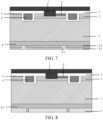
FIG. 4 to FIG. 7 are schematic diagrams of corresponding structures formed according to preparation steps ofEmbodiment 1 of the present disclosure; -
FIG. 8 to FIG. 10 are schematic diagrams of corresponding structures formed according to preparation steps ofEmbodiment 2 of the present disclosure; -
FIG. 11 is a schematic diagram of simulated forward conduction characteristic curves of a conventional reverse conducting IGBT power device according to an embodiment of the present disclosure and a reverse conducting IGBT power device according toEmbodiment 1; and -
FIG. 12 is a schematic block diagram of an electronic device according to an embodiment of the present disclosure. - N+ collector region 8' and P+ collector region 9'; and
The present disclosure: - reverse conducting
IGBT power device 100;electronic device 1000;front side 1011; -
drift region 1,active region 2,gate oxide layer 3,polysilicon gate 4,dielectric layer 5,emitter region 6,emitter 7, field-stop layer 8-1, field-stop layer 8-2, collector insertion layer 9-1, second collector layer 9-2, collector interconnection portion 9-3, andfirst collector layer 10. - The following describes embodiments of the present disclosure in detail. Examples of the embodiments are shown in the accompanying drawings, and same or similar reference signs in all the accompanying drawings indicate same or similar components or components having same or similar functions. The embodiments described below with reference to the accompanying drawings are exemplary, and are intended to explain the present disclosure and cannot be construed as a limitation to the present disclosure.
- The following describes a reverse conducting IGBT power device according to an embodiment of a first aspect of the present disclosure with reference to the accompanying drawings.
- The reverse conducting IGBT power device in this embodiment of the present disclosure includes at least one cell.
FIG. 2 is a schematic diagram of a structure of a cell of a reverse conducting IGBT power device according to an embodiment of the present disclosure. - In this embodiment of the present disclosure, a cell of the reverse conducting
IGBT power device 100 includes anelectric field region 101 of a first conductivity type. A front structure is formed on afront side 1011 of theelectric field region 101. As shown inFIG. 2 , the front structure may include anemitter 7, anemitter region 6, anactive region 2, and a gate structure (3 and 4). Theemitter 7 is in ohmic contact with both theemitter region 6 and theactive region 2, and the gate structure (3 and 4) is insulated from theemitter 7, theemitter region 6, theactive region 2, and the electric field region 101 (for example, insulated by a dielectric layer 5). A collector structure is arranged on a back side of theelectric field region 101. - In some embodiments, the
electric field region 101 may be adrift region 1. Alternatively, as shown inFIG. 2 , theelectric field region 101 includes adrift region 1 and a field-stop layer 8 (or referred to as a buffer layer), and the field-stop layer 8 is in contact with a lower surface of thedrift region 1. That is, the reverse conductingIGBT power device 100 in this embodiment of the present disclosure may be of a punch-through structure or a non-punch-through structure. The electric field region may be of a non-punch-through (NPT) structure, a punch-through (PT) structure, a soft punch-through (SPT) structure, or a field-stop (FS) structure, which is not specifically limited. - In this embodiment, the gate structure may be a trench gate structure, as shown in
FIG. 2 . The trench gate structure includes a gate groove of thedrift region 1. Apolysilicon gate 4 and agate oxide layer 3 are arranged in the gate groove, and thepolysilicon gate 4 is insulated from other structures by thedielectric layer 5. In some embodiments, a dielectric material of thedielectric layer 5 may be a high-k dielectric material such as SiO2, HfO2, Al2O3, or Si3N4. The gate structure may alternatively be a planar gate structure, which is not specifically limited herein. - As shown in
FIG. 2 , different from a structure of the existing reverse conducting IGBT power device, a collector structure of the reverse conductingIGBT power device 100 in this embodiment of the present disclosure includes afirst collector layer 10 of a first conductivity type, a second collector layer 9-2 of a second conductivity type, a collector insertion layer 9-1 (only one layer is shown inFIG. 2 as an example), a collector interconnection portion 9-3, and a collector (not shown). The second collector layer 9-2 and thefirst collector layer 10 are located on a lower surface of theelectric field region 101, for example, a lower surface of the drift region or the field-stop region. The second collector layer 9-2 is in contact with thefirst collector layer 10. Both the second collector layer 9-2 and thefirst collector layer 10 are connected to the collector. The collector insertion layer 9-1 is located in theelectric field region 101, for example, in thedrift region 1 or the field-stop layer 8. The collector insertion layer 9-1 is connected to the second collector layer 9-2 by the collector interconnection portion 9-3, that is, the collector is connected. - In some embodiments of the present disclosure, For the punch-through structure, the
electric field region 101 is adrift region 1, and the collector insertion layer 9-1 is arranged in thedrift region 1; and for the non-punch-through structure, theelectric field region 101 includes thedrift region 1 and the field-stop layer 8 (or referred to as a buffer layer), and the collector insertion layer 9-1 is arranged in the field-stop layer 8, as shown inFIG. 2 . - In this embodiment, the first conductivity type may be N-type, and the second conductivity type is P-type; or the first conductivity type may be P-type, and the second conductivity type is N-type. The collector structure in this embodiment of the present disclosure is applicable to an N-channel reverse conducting IGBT power device, and is also applicable to a P-channel reverse conducting IGBT power device. For ease of description, an N-channel reverse conducting IGBT power device is used as an example in the embodiments of the present disclosure, the first conductivity type is N-type, and the second conductivity type is P-type.
- As shown in
FIG. 2 , theelectric field region 101 includes an N-drift region 1 and an N-type field-stop layer 8. The collector structure includes an N+first collector layer 10 and a P+ collector layer. The P+ collector layer may be a double-layer or multi-layer interconnection structure. The P+ collector layer includes a P+ collector insertion layer 9-1. There may be one or more collector insertion layers 9-1 (one layer is shown inFIG. 2 ), and the collector insertion layer 9-1 is connected to the second collector layer 9-2 by the P+ collector interconnection portion 9-3, which is equivalent to extending a length of the P+ collector layer in a transverse direction of the power device. - When the power device is conducted forward, an electron path passes from the
drift region 1 to the field-stop layer 8, and then reaches the first collector such as the N+first collector layer 10 by transversely bypassing the collector insertion layer 9-1, which is equivalent to prolonging a path for collecting electrons by the collector. A potential difference can be increased faster to meet a requirement for junction conduction between the second collector layer 9-2 and the electric field region such as thedrift region 1 or the field-stop layer 8, and switching to an IGBT mode faster can be made, thereby reducing a voltage snapback, and suppressing a negative differential resistance effect. - In the reverse conducting
IGBT power device 100 in this embodiment of the present disclosure, the collector insertion layer 9-1 is arranged in the electric field region, and the collector insertion layer 9-1 is connected to the second collector layer 9-2 by the collector interconnection portion 9-3, so that a length of the second collector layer 9-2 in a transverse direction of the power device is extended. When the reverse conductingIGBT power device 100 is conducted forward, an electron path needs to transversely bypass the collector insertion layer 9-1 to reach the first collector such as the N+first collector layer 10, which is equivalent to prolonging a path for collecting electrons by the collector. A potential difference can be increased faster to meet a requirement for junction conduction between the second collector layer 9-2 and the electric field region, and the PN junction is conducted forward faster, thereby reducing a voltage snapback and suppressing a negative differential resistance effect. The structure does not degrade other performance of the device either. - In some embodiments of the present disclosure, the semiconductor power device includes a plurality of cells arranged in a transverse direction of the power device, and collector insertion layers 9-1 and second collector layers 9-2 of two adjacent cells overlap in a longitudinal direction of the power device, as shown in
FIG. 2 . In this way, a length of the P+ collector layer in the transverse direction of the power device can be increased, a negative differential resistance effect is effectively suppressed, and overall distribution of the second collector layers 9-2 is not affected. Certainly, the collector insertion layers and the second collector layers may alternatively not overlap. To be specific, the second collector layer 9-2, the collector insertion layer 9-1, and the collector interconnection portion 9-3 of each cell form a collector interconnection structure, and collector interconnection structures of two adjacent cells are distributed in parallel in a transverse direction of the power device. That is, the collector insertion layers 9-1 and the second collector layers 9-2 do not overlap. - In some embodiments, the collector structure includes a plurality of collector insertion layers 9-1, that is, there may be a plurality of collector insertion layers 9-1. The plurality of collector insertion layers 9-1 are arranged in the longitudinal direction of the power device, and each collector insertion layer 9-1 is connected to the second collector layer 9-2 by the collector interconnection portion 9-3. Lengths of the plurality of collector insertion layers 9-1 in the transverse direction of the power device may vary, so that a length of the second collector layer 9-2 can be further increased, and the negative differential resistance effect can be effectively suppressed.
- In some embodiments, there may alternatively be one collector insertion layer 9-1, and there is a preset distance between the collector insertion layer 9-1 and the second collector layer 9-2, for example, 2.5 micrometers to 3.5 micrometers. The collector insertion layer 9-1 is connected to the second collector layer 9-2 by the collector interconnection portion 9-3. One end of the collector interconnection portion 9-3 is connected to an end portion or a middle portion of the collector insertion layer 9-1, and the other end of the collector interconnection portion 9-3 is connected to an end portion or a middle portion of the second collector layer 9-2. For example, one end of the collector interconnection portion 9-3 is connected to the middle portion of the collector insertion layer 9-1 and the other end of the collector interconnection portion 9-3 is connected to the middle portion of the second collector layer 9-2, or one end of the collector interconnection portion 9-3 is connected to one end of the collector insertion layer 9-1 and the other end of the collector interconnection portion 9-3 is connected to the middle portion of the second collector layer 9-2, or one end of the collector interconnection portion 9-3 is connected to the middle portion of the collector insertion layer 9-1 and the other end of the collector interconnection portion 9-3 is connected to one end of the second collector layer 9-2. As shown in
FIG. 2 , the collector interconnection portion 9-3 is connected to one end of the collector insertion layer 9-1, and the collector interconnection portion 9-3 is connected to one end of the second collector layer 9-2, so that a length of the P+ collector layer in the transverse direction of the power device can be increased, an electron path of the collector can be extended, and a negative differential resistance effect can be effectively suppressed. - The structure of the reverse conducting
IGBT power device 100 in this embodiment of the present disclosure is described above. In the reverse conductingIGBT power device 100 in this embodiment of the present disclosure, the collector interconnection structure of the collector insertion layer 9-1, the collector interconnection portion 9-3, and the second collector 9-2 is arranged, so that a length of the second collector in the transverse direction of the power device is increased, an electron path is extended, and a negative differential resistance effect can be effectively suppressed. - In some examples of the present disclosure, the front structure and the back-side structure may be prepared through processes such as photolithography, epitaxy, oxidation, ion injection, and deposition on a substrate made of a semiconductor material such as Si, SiC, GaAs, or GaN. A method for preparing the reverse conducting IGBT power device in the embodiments of the present disclosure is described below.
-
FIG. 3 is a flowchart of a method for preparing a reverse conducting IGBT power device according to an embodiment of the present disclosure. As shown inFIG. 3 , the method includes:
S1: A substrate is provided. - The substrate has an electric field region. In some embodiments, the electric field region may be a drift region, that is, a punch-through structure is used. Alternatively, the electric field region may include a drift region and a field-stop region (or referred to as a buffer region), that is, a non-punch-through structure is used.
- In this embodiment, an original substrate may be provided, and a drift region of the first conductivity type is formed on a front side of the original substrate, where the drift region is the electric field region. That is, the drift region is prepared on the front side of the original substrate before a front structure and a back side structure are prepared. Certainly, for a non-punch-through structure, the field-stop layer may also be prepared through ion injection in a subsequent preparation step.
- Alternatively, an original substrate is provided, a drift region of the first conductivity type is formed on a front side of the original substrate, and forming a field-stop layer of the first conductivity type on a back side of the original substrate, where the drift region and the field-stop layer are the electric field region. That is, the drift region is prepared on the front side of the original substrate and the field-stop region is prepared on the back side before a front structure and a back side structure are prepared.
- Alternatively, a substrate having a drift region of the first conductivity type and a field-stop layer of the first conductivity type are directly provided, where the drift region and the field-stop layer are the electric field region. For example, a double-layer epitaxial material having an N-type field-stop layer and an N-drift region may be directly selected as a silicon wafer material for the start of a process, that is, an original substrate. Therefore, an FS field-stop layer formed through ion injection is not required in a subsequent process.
- In some embodiments, the original substrate may be made of Si, SiC, GaAs, or GaN.
- S2: A front structure is prepared through photolithography, oxidation, ion injection, and deposition on a front side of the electric field region.
- In some embodiments, the front structure may include at least an emitter, an emitter region, an active region, and a gate structure. The emitter is in ohmic contact with both the emitter region and the active region, and the gate structure is insulated from the emitter, the emitter region, and the active region.
- S3: A first collector layer of a first conductivity type and a second collector layer of a second conductivity type are prepared on a lower surface of the electric field region through photolithography, ion injection, and epitaxy on a back side of the electric field region, and a collector insertion layer and a collector interconnection portion that are of the second conductivity type are prepared in the electric field region, where the collector insertion layer is electrically connected to the second collector layer by the collector interconnection portion.
- In this embodiment, For the punch-through structure, the front structure is prepared above the drift region, the collector insertion layer is prepared in the drift region, and the collector interconnection portion and the second collector layer are prepared through ion injection, so that the collector insertion layer is connected to the second collector layer.
- S4: A metal electrode is prepared on lower surfaces of the first collector layer and the second collector layer to form a collector, that is, a back electrode.
- According to the method for preparing a reverse conducting IGBT power device in this embodiment of the present disclosure, the collector insertion layer is prepared in the electric field region, and the collector insertion layer is electrically connected to the second collector layer by the collector interconnection portion, so that a length of the second collector layer in a transverse direction of the power device is increased. When the reverse conducting IGBT power device is conducted forward, a path for collecting electrons by the collector is extended, and a potential difference can be increased faster to meet a requirement for junction conduction between the second collector layer and the electric field region. A PN junction is conducted forward faster, and a voltage snapback is reduced, thereby suppressing a negative differential resistance effect. Other performance of the power device is not degraded.
- In some embodiments, the collector structure may be prepared by using an epitaxial layer. Specifically, a mask of the collector insertion layer is prepared through photolithography on the back side of the electric field region, and the collector insertion layer of the second conductivity type is formed through ion injection; an epitaxial layer of a same doping type as that of the electric field region is formed through epitaxy on a lower surface of the substrate on which the collector insertion layer is prepared; the second collector layer of the second conductivity type is formed through ion injection on the epitaxial layer, and the collector interconnection portion of the second conductivity type is formed through ion injection to connect the second collector layer and the collector insertion layer; and photolithography, ion injection, and epitaxy are performed on the second collector layer to prepare the first collector layer of the first conductivity type in contact with the epitaxial layer and the second collector layer.
- The method for preparing a reverse conducting IGBT power device in this embodiment of the present disclosure is described below by using an N-channel non-punch-through structure such as an FS-type structure as an example.
- Embodiment 1: A trench-type FS reverse conducting IGBT power device with a voltage level of 750 V is used as an example, and a structure of a cell thereof is shown in
FIG. 2 . Referring toFIG. 4 to FIG. 7 , a method for preparing the same includes the following steps: - First step: As shown in
FIG. 4 , an N-type silicon substrate with a thickness ranging from 300 micrometers to 500 micrometers is selected, and the substrate is lightly doped to form an N-drift region 1; and anemitter 7, anemitter region 6, anactive region 2, and a gate structure (3 and 4) in a cell of the reverse conducting IGBT power device are prepared on a front side of the silicon substrate through a plurality of photolithography, oxidation, ion injection, annealing, and deposition processes above thedrift region 1, and insulation treatment is performed through adielectric layer 5. A specific process for the gate structure being a trench gate structure is a trench gate structure process. - Second step: The silicon substrate is flipped, and a back side of a silicon wafer is thinned, to cause a thickness of the silicon wafer to range from 70 micrometers to 80 micrometers, for example, 77 micrometers.
- Third step: As shown in
FIG. 4 , photolithography is performed, a P+ mask is prepared in a partial region of the back side of the substrate, and a P+ collector insertion layer 9-1 is prepared on the back side through ion injection. A thickness of the formed collector insertion layer 9-1 may be 0.2 micrometers, an ion injection energy is 40 KeV, and an injection dose is 2 × 10¹³/cm2. - Fourth step: As shown in
FIG. 5 ,3 micrometers of N-type silicon 8-2 with the same dopant as that of the substrate is deposited on the back side. - Fifth step: As shown in
FIG. 6 , a P+ second collector layer 9-2 connected to a metal electrode, that is, a collector, is prepared on the back side through ion injection. A thickness of the formed second collector layer 9-2 is 0.2 micrometers. An ion injection energy may be 40 KeV, and an injection dose may be 2 × 10¹³/cm2. - Sixth step: As shown in
FIG. 7 , photolithography is performed, a mask of a P+ collector interconnection portion 9-3 is prepared on the back side, and the P+ collector insertion layer 9-1 and the P+ second collector layer 9-2 are connected through ion injection, to form an interconnected P+ collector region. - Seventh step: As shown in
FIG. 2 , photolithography is performed, a mask of an N+first collector layer 10 is prepared on the back side, and the N+first collector layer 10 is prepared on the back side through ion injection. A thickness of the formed N+first collector layer 10 is 0.2 micrometers, an ion injection energy is 40 KeV, and an injection dose is 2 × 10¹³/cm2. - Eighth step: Field-stop layers including a field-stop layer 8-1 and a field-stop layer 8-2 are formed on the back side of the cell through ion injection.
- Ninth step: Metal is deposited on the back side to form a metal collector, that is, a back electrode.
- A trench-type FS reverse conducting IGBT power device having an overlapping P+ collector interconnection structure shown in
FIG. 2 can be prepared through the foregoing preparing method. It may be understood that the process steps and the process conditions in the foregoing preparation method may be set according to an actual requirement, and a sequence of the process steps may also be adjusted or changed based on the actual requirement. - In some other embodiments of the present disclosure, the reverse conducting IGBT power device in this embodiment of the present disclosure may alternatively be prepared without forming an epitaxial layer through epitaxy, and may alternatively be prepared through deep ion injection.
- Specifically, an injection layer of the second conductivity type is formed through photolithography and ion injection on the back side of the electric field region, and photolithography, masking, and ion injection are performed on the injection layer to form the collector insertion layer inside the electric field region and form the collector interconnection portion connected to the collector insertion layer; the second collector layer of the second conductivity type is prepared through ion injection on a surface of the back side of the electric field region in which the collector insertion layer and the collector interconnection portion are formed, where the second collector layer is connected to the collector interconnection portion; and the first collector layer of the first conductivity type is formed through photolithography and ion injection on the second collector layer.
- The method for preparing a reverse conducting IGBT power device in this embodiment of the present disclosure is described below by still using an N-channel non-punch-through structure such as an FS-type structure as an example.
- Embodiment 2: Similarly, a FS reverse conducting IGBT power device with a voltage level of 750 V is used as an example, and a structure of a cell thereof is shown in
FIG. 2 . A difference is that epitaxy is not performed on deposited silicon on a back side in this embodiment. Referring toFIG. 8 to FIG. 10 , a method for preparing the same includes the following steps: - First step: As shown in
FIG. 8 , an N-type silicon substrate with a thickness ranging from 300 micrometers to 500 micrometers is selected, and the substrate is lightly doped to form an N-drift region 1; and anemitter 7, anemitter region 6, anactive region 2, and a gate structure (3 and 4) in a cell of the reverse conducting IGBT power device are prepared on a front side of the silicon wafer through a plurality of photolithography, oxidation, ion injection, annealing, and deposition processes above thedrift region 1, and insulation treatment is performed through adielectric layer 5. A specific process for the gate structure being a trench gate structure is a trench gate structure process. - Second step: The silicon substrate is flipped, a back side of a silicon wafer is thinned, to cause a thickness of the silicon wafer to range, for example, from 70 micrometers to 80 micrometers, and an N-field-stop layer 8-1 is formed on the back side of the substrate through hydrogen injection.
- Third step: As shown in
FIG. 8 , photolithography is performed, a mask of a P+ collector insertion layer is prepared, and aninjection layer 9 is prepared through ion injection. - Fourth step: As shown in
FIG. 9 , photolithography is performed on theinjection layer 9, a mask of an N-field-stop layer 8-2 is prepared, the N-field-stop layer 8-2 with the same dopant as that of the N-field-stop layer 8-1 is prepared through ion injection, and a P+ collector insertion layer 9-1 and a P+ collector interconnection portion 9-3 connected to the P+ collector insertion layer 9-1 are formed. The P+ collector insertion layer 9-1 is deep. - Fifth step: As shown in
FIG. 10 , a P+ second collector layer 9-2 connected to a metal collector is prepared through ion injection. - Sixth step: As shown in
FIG. 2 , a mask of an N+first collector layer 10 is prepared through photolithography, and the N+second collector 10 is prepared through ion injection. - Seventh step: Metal is deposited on the back side to form a metal collector, that is, a back electrode.
- A trench-type FS reverse conducting IGBT power device having an overlapping P+ collector interconnection structure shown in
FIG. 2 can be prepared through the foregoing preparing method. It may be understood that the process steps and the process conditions in the foregoing preparation method may be set according to an actual requirement, and a sequence of the process steps may also be adjusted or changed based on the actual requirement. - A simulation test is performed based on
Embodiment 1. Specifically, two structures of the conventional reverse conducting IGBT power device and the reverse conducting IGBT power device inEmbodiment 1 are designed through simulation. The two structures have identical front-side emitters, emitter regions, and gate structures. An N+ first collector layer and a P+ second collector layer in a back-side collector region that are in contact with a metal collector have a same width. A width of the N+ first collector layer is 3 micrometers, and a width of the P+ second collector layer is 19.2 micrometers. The P+ collector insertion layer 9-1 and the P+ second collector layer 9-2 in this embodiment of the present disclosure are spaced apart by 3 micrometers. -
FIG. 11 is a schematic diagram of forward conduction characteristic curves obtained through simulation of a conventional reverse conducting IGBT power device and a reverse conducting IGBT power device according toEmbodiment 1. The accompanying drawing shows an enlarged view at the beginning of conduction of the power devices. It can be seen that the negative differential resistance phenomenon of the conventional reverse conducting IGBT power device reaches 48 V, while the negative differential resistance phenomenon of the reverse conducting IGBT power device obtained inEmbodiment 1 of the present disclosure is 9 V, which reduces the negative differential resistance effect by more than 80%, and effectively suppresses the negative differential resistance effect. - An embodiment of a third aspect of the present disclosure further provides an
electronic device 1000. As shown inFIG. 12 , theelectronic device 1000 includes at least one reverse conductingIGBT power device 100 according to any embodiment of the first aspect of the present disclosure. Theelectronic device 1000 may be a motor controller, an on-board charger, or the like. The reverse conductingIGBT power device 100 is configured to drive, convert an electrical signal, or the like. - In the
electronic device 1000 in this embodiment of the present disclosure, by using the reverse conducting IGBT power device in the foregoing embodiments, a voltage snapback phenomenon is reduced, a negative differential resistance effect can be effectively suppressed, and product performance is improved. - The foregoing descriptions are merely two specific implementations of the present disclosure, and any feature disclosed in this specification may be replaced with another equivalent or replaceable feature having a similar purpose. All disclosed features, or steps in all disclosed methods or processes can be combined in any mode except for the mutually exclusive features or steps.
- In description of the present disclosure, description of reference terms such as "one embodiment", "some embodiments", "example", "specific example", or "some examples" means including specific features, structures, materials, or features described in the embodiment or example in at least one embodiment or example of the present disclosure. In this specification, exemplary description of the foregoing terms does not necessarily refer to a same embodiment or example. Moreover, the specific feature, structure, material, or characteristic described may be combined in any one or more embodiments or examples in a suitable manner. In addition, with no conflict, a person skilled in the art may integrate or combine different embodiments or examples described in the specification and features of the different embodiments or examples.
- Although the embodiments of the present disclosure are shown and described above, it can be understood that, the foregoing embodiments are exemplary, and cannot be construed as a limitation to the present disclosure. Within the scope of the present disclosure, a person of ordinary skill in the art may make changes, modifications, replacement, and variations to the foregoing embodiments.
Claims (15)
- A reverse conducting IGBT power device (100), the reverse conducting IGBT power device (100) comprising at least one cell, and the cell comprising:an electric field region (101) of a first conductivity type, a front structure being formed on a front side (1011) of the electric field region (101), and a collector structure being arranged on a back side of the electric field region (101);wherein the collector structure comprises:a first collector layer (10) of the first conductivity type;a second collector layer (9-2) of a second conductivity type;a collector insertion layer (9-1);a collector interconnection portion (9-3); anda collector, the second collector layer (9-2) and the first collector layer (10) being located on a lower surface of the electric field region (101), the second collector layer (9-2) being in contact with the first collector layer (10), both the second collector layer (9-2) and the first collector layer (10) being connected to the collector, the collector insertion layer (9-1) being located in the electric field region (101), and the collector insertion layer (9-1) being connected to the second collector layer (9-2) by the collector interconnection portion (9-3).
- The reverse conducting IGBT power device (100) according to claim 1, wherein the electric field region (101) is a drift region (1), and the collector insertion layer (9-1) is arranged in the drift region (1).
- The reverse conducting IGBT power device (100) according to claim 1, wherein the electric field region (101) comprises:a drift region (1); anda field-stop layer (8), wherein the field-stop layer (8) is in contact with a lower surface of the drift region (1), and the collector insertion layer (9-1) is arranged in the field-stop layer (8).
- The reverse conducting IGBT power device (100) according to any one of claims 1 to 3, the reverse conducting IGBT power device (100) comprising a plurality of cells arranged in a transverse direction of the reverse conducting IGBT power device (100), and collector insertion layers (9-1) and second collector layers (9-2) of two adjacent cells overlap in the transverse direction of the reverse conducting IGBT power device (100).
- The reverse conducting IGBT power device (100) according to any one of claims 1 to 3, the reverse conducting IGBT power device (100) comprising a plurality of cells arranged in a transverse direction of the reverse conducting IGBT power device (100); and
the second collector layer (9-2), the collector insertion layer (9-1), and the collector interconnection portion (9-3) of each of the cells form a collector interconnection structure, and collector interconnection structures of two adjacent cells are distributed in parallel in a transverse direction of the reverse conducting IGBT power device (100). - The reverse conducting IGBT power device (100) according to any one of claims 1 to 5, wherein the collector structure comprises a plurality of collector insertion layers (9-1), the plurality of collector insertion layers (9-1) are arranged in a longitudinal direction of the reverse conducting IGBT power device (100), and each of the collector insertion layers (9-1) is connected to the second collector layer (9-2) by the collector interconnection portion (9-3).
- The reverse conducting IGBT power device (100) according to any one of claims 1 to 6, wherein a preset distance is provided between the collector insertion layer (9-1) and the second collector layer (9-2), one end of the collector interconnection portion (9-3) is connected to an end portion or a middle portion of the collector insertion layer (9-1), and the other end of the collector interconnection portion (9-3) is connected to an end portion or a middle portion of the second collector layer (9-2).
- The reverse conducting IGBT power device (100) according to claim 7, wherein the preset distance is in a range of 2.5 micrometers to 3.5 micrometers.
- The reverse conducting IGBT power device (100) according to any one of claims 1 to 8, whereinthe first conductivity type is N-type, and the second conductivity type is P-type; orthe first conductivity type is P-type, and the second conductivity type is N-type.
- A method for preparing a reverse conducting IGBT power device, comprising:providing a substrate, wherein the substrate has an electric field region;preparing a front structure through photolithography, oxidation, ion injection, and deposition on a front side of the electric field region;preparing a first collector layer of a first conductivity type and a second collector layer of a second conductivity type on a lower surface of the electric field region through photolithography, ion injection, and epitaxy on a back side of the electric field region, and preparing a collector insertion layer and a collector interconnection portion that are of the second conductivity type in the electric field region, wherein the collector insertion layer is electrically connected to the second collector layer by the collector interconnection portion; andpreparing a metal electrode on lower surfaces of the first collector layer and the second collector layer to form a collector.
- The method for preparing a reverse conducting IGBT power device according to claim 10, wherein providing the substrate comprises:providing an original substrate, and forming a drift region of the first conductivity type on a front side of the original substrate, wherein the drift region is the electric field region; orproviding an original substrate, forming a drift region of the first conductivity type on a front side of the original substrate, and forming a field-stop layer of the first conductivity type on a back side of the original substrate, wherein the drift region and the field-stop layer are the electric field region; orproviding a substrate having a drift region of the first conductivity type and a field-stop layer of the first conductivity type, wherein the drift region and the field-stop layer are the electric field region.
- The method for preparing a reverse conducting IGBT power device according to claim 11, wherein preparing the first collector layer of the first conductivity type, and the second collector layer, the collector insertion layer, and the collector interconnection portion that are of the second conductivity type through photolithography, ion injection, and epitaxy on the back side of the electric field region comprises:preparing a mask of the collector insertion layer through photolithography on the back side of the electric field region, and forming the collector insertion layer of the second conductivity type through ion injection;forming, through epitaxy, an epitaxial layer of a same doping type as that of the electric field region on a lower surface of the substrate on which the collector insertion layer is prepared;forming the second collector layer of the second conductivity type through ion injection on the epitaxial layer, and forming the collector interconnection portion of the second conductivity type through ion injection to connect the second collector layer and the collector insertion layer; andperforming photolithography, ion injection, and epitaxy on the second collector layer to prepare the first collector layer of the first conductivity type that is in contact with the epitaxial layer and the second collector layer.
- The method for preparing a reverse conducting IGBT power device according to claim 11, wherein preparing the first collector layer of the first conductivity type, and the second collector layer, the collector insertion layer, and the collector interconnection portion that are of the second conductivity type through photolithography and ion injection on the back side of the electric field region comprises:forming an injection layer of the second conductivity type through photolithography and ion injection on the back side of the electric field region, and performing photolithography, masking, and ion injection on the injection layer to form the collector insertion layer inside the electric field region and form the collector interconnection portion connected to the collector insertion layer;preparing the second collector layer of the second conductivity type through ion injection on a surface of the back side of the electric field region in which the collector insertion layer and the collector interconnection portion are formed, wherein the second collector layer is connected to the collector interconnection portion; andforming the first collector layer of the first conductivity type through photolithography and ion injection on the second collector layer.
- The method for preparing a reverse conducting IGBT power device according to any one of claims 11 to 13, wherein the original substrate is made of Si, SiC, GaAs, or GaN.
- An electronic device (1000), comprising at least one reverse conducting IGBT power device (100) according to any one of claims 1 to 9.
Applications Claiming Priority (2)
| Application Number | Priority Date | Filing Date | Title |
|---|---|---|---|
| CN202210999420.XA CN117637820A (en) | 2022-08-19 | 2022-08-19 | Reverse conduction IGBT power device and preparation method and electronic equipment thereof |
| PCT/CN2023/102381 WO2024037186A1 (en) | 2022-08-19 | 2023-06-26 | Reverse conducting igbt power device and preparation method therefor, and electronic device |
Publications (2)
| Publication Number | Publication Date |
|---|---|
| EP4576223A1 true EP4576223A1 (en) | 2025-06-25 |
| EP4576223A4 EP4576223A4 (en) | 2025-11-26 |
Family
ID=89940602
Family Applications (1)
| Application Number | Title | Priority Date | Filing Date |
|---|---|---|---|
| EP23854091.8A Pending EP4576223A4 (en) | 2022-08-19 | 2023-06-26 | Backward-facing IGBT power device and manufacturing method therefor and electronic device |
Country Status (4)
| Country | Link |
|---|---|
| US (1) | US20250185351A1 (en) |
| EP (1) | EP4576223A4 (en) |
| CN (1) | CN117637820A (en) |
| WO (1) | WO2024037186A1 (en) |
Family Cites Families (8)
| Publication number | Priority date | Publication date | Assignee | Title |
|---|---|---|---|---|
| GB2150753B (en) * | 1983-11-30 | 1987-04-01 | Toshiba Kk | Semiconductor device |
| US9018674B2 (en) * | 2012-04-06 | 2015-04-28 | Infineon Technologies Ag | Reverse conducting insulated gate bipolar transistor |
| JP6119577B2 (en) * | 2013-11-26 | 2017-04-26 | 三菱電機株式会社 | Semiconductor device |
| JP5920383B2 (en) * | 2014-03-03 | 2016-05-18 | トヨタ自動車株式会社 | Method for manufacturing semiconductor device and semiconductor device |
| JP2016058428A (en) * | 2014-09-05 | 2016-04-21 | 株式会社東芝 | Semiconductor device |
| CN109979935B (en) * | 2017-12-28 | 2025-04-22 | 富士电机株式会社 | Semiconductor device and method for manufacturing semiconductor device |
| CN108649068B (en) * | 2018-06-29 | 2021-07-09 | 中国科学院微电子研究所 | RC-IGBT device and preparation method thereof |
| CN112466935B (en) * | 2020-12-15 | 2023-03-14 | 重庆邮电大学 | RC-IGBT device with polycrystalline silicon electronic channel of collector electrode |
-
2022
- 2022-08-19 CN CN202210999420.XA patent/CN117637820A/en active Pending
-
2023
- 2023-06-26 WO PCT/CN2023/102381 patent/WO2024037186A1/en not_active Ceased
- 2023-06-26 EP EP23854091.8A patent/EP4576223A4/en active Pending
-
2025
- 2025-02-12 US US19/051,984 patent/US20250185351A1/en active Pending
Also Published As
| Publication number | Publication date |
|---|---|
| WO2024037186A1 (en) | 2024-02-22 |
| CN117637820A (en) | 2024-03-01 |
| EP4576223A4 (en) | 2025-11-26 |
| US20250185351A1 (en) | 2025-06-05 |
Similar Documents
| Publication | Publication Date | Title |
|---|---|---|
| US7157785B2 (en) | Semiconductor device, the method of manufacturing the same, and two-way switching device using the semiconductor devices | |
| KR100214207B1 (en) | Semiconductor device and manufacturing method thereof | |
| US20230307529A1 (en) | Support shield structures for trenched semiconductor devices | |
| CN110600537B (en) | A split gate CSTBT with PMOS current clamping and its fabrication method | |
| US20120049270A1 (en) | Method for Forming a Semiconductor Device, and a Semiconductor with an Integrated Poly-Diode | |
| CN107731898B (en) | CSTBT device and manufacturing method thereof | |
| CN106997899B (en) | A kind of IGBT device and preparation method thereof | |
| CN112201690B (en) | MOSFET Transistor | |
| CN107808899A (en) | Lateral power with hybrid conductive pattern and preparation method thereof | |
| CN110518058A (en) | A kind of lateral trench type insulated gate bipolar transistor and preparation method thereof | |
| WO2023112547A1 (en) | Semiconductor device | |
| JP2003303965A (en) | Semiconductor device and manufacturing method thereof | |
| CN110504260B (en) | Transverse groove type IGBT with self-bias PMOS and preparation method thereof | |
| EP4708353A1 (en) | Igbt device and cellular structure thereof, and manufacturing method for cellular structure | |
| CN109065608B (en) | A kind of lateral bipolar power semiconductor device and preparation method thereof | |
| CN110504313B (en) | A lateral trench type insulated gate bipolar transistor and its preparation method | |
| JPH1140808A (en) | Semiconductor device and manufacturing method thereof | |
| CN108155230B (en) | Transverse RC-IGBT device and preparation method thereof | |
| CN115064584A (en) | A trench gate IGBT device with carrier storage layer | |
| CN110459596B (en) | Transverse insulated gate bipolar transistor and preparation method thereof | |
| EP4576223A1 (en) | Reverse conducting igbt power device and preparation method therefor, and electronic device | |
| Zhang et al. | 41% Reduction In Power Stage Area On Silicon-On-Insulator Bipolar-CMOS-DMOS-IGBT Platform With Newly Developed Multiple Deep-Oxide Trench Technology | |
| CN213459746U (en) | MOSFET transistor | |
| CN113838915B (en) | Trench gate charge storage type IGBT and manufacturing method thereof | |
| CN114651335B (en) | Insulated Gate Bipolar Transistor |
Legal Events
| Date | Code | Title | Description |
|---|---|---|---|
| STAA | Information on the status of an ep patent application or granted ep patent |
Free format text: STATUS: THE INTERNATIONAL PUBLICATION HAS BEEN MADE |
|
| PUAI | Public reference made under article 153(3) epc to a published international application that has entered the european phase |
Free format text: ORIGINAL CODE: 0009012 |
|
| STAA | Information on the status of an ep patent application or granted ep patent |
Free format text: STATUS: REQUEST FOR EXAMINATION WAS MADE |
|
| 17P | Request for examination filed |
Effective date: 20250318 |
|
| AK | Designated contracting states |
Kind code of ref document: A1 Designated state(s): AL AT BE BG CH CY CZ DE DK EE ES FI FR GB GR HR HU IE IS IT LI LT LU LV MC ME MK MT NL NO PL PT RO RS SE SI SK SM TR |
|
| REG | Reference to a national code |
Ref country code: DE Ref legal event code: R079 Free format text: PREVIOUS MAIN CLASS: H01L0029417000 Ipc: H10D0010010000 |
|
| A4 | Supplementary search report drawn up and despatched |
Effective date: 20251027 |
|
| DAV | Request for validation of the european patent (deleted) | ||
| DAX | Request for extension of the european patent (deleted) | ||
| RIC1 | Information provided on ipc code assigned before grant |
Ipc: H10D 10/01 20250101AFI20251021BHEP Ipc: H10D 12/00 20250101ALI20251021BHEP Ipc: H10D 12/01 20250101ALI20251021BHEP Ipc: H10D 62/13 20250101ALI20251021BHEP Ipc: H10D 62/17 20250101ALI20251021BHEP Ipc: H10D 84/00 20250101ALI20251021BHEP Ipc: H10D 84/80 20250101ALI20251021BHEP |