EP4576149A2 - Elektrisches verbindungssystem - Google Patents
Elektrisches verbindungssystem Download PDFInfo
- Publication number
- EP4576149A2 EP4576149A2 EP25174125.2A EP25174125A EP4576149A2 EP 4576149 A2 EP4576149 A2 EP 4576149A2 EP 25174125 A EP25174125 A EP 25174125A EP 4576149 A2 EP4576149 A2 EP 4576149A2
- Authority
- EP
- European Patent Office
- Prior art keywords
- array
- electron
- pneumatic actuator
- electrical contact
- lever
- Prior art date
- Legal status (The legal status is an assumption and is not a legal conclusion. Google has not performed a legal analysis and makes no representation as to the accuracy of the status listed.)
- Pending
Links
Images


Classifications
-
- H—ELECTRICITY
- H01—ELECTRIC ELEMENTS
- H01H—ELECTRIC SWITCHES; RELAYS; SELECTORS; EMERGENCY PROTECTIVE DEVICES
- H01H35/00—Switches operated by change of a physical condition
- H01H35/24—Switches operated by change of fluid pressure, by fluid pressure waves, or by change of fluid flow
- H01H35/32—Switches operated by change of fluid pressure, by fluid pressure waves, or by change of fluid flow actuated by bellows
-
- H—ELECTRICITY
- H01—ELECTRIC ELEMENTS
- H01H—ELECTRIC SWITCHES; RELAYS; SELECTORS; EMERGENCY PROTECTIVE DEVICES
- H01H1/00—Contacts
- H01H1/12—Contacts characterised by the manner in which co-operating contacts engage
- H01H1/14—Contacts characterised by the manner in which co-operating contacts engage by abutting
- H01H1/32—Self-aligning contacts
-
- H—ELECTRICITY
- H01—ELECTRIC ELEMENTS
- H01J—ELECTRIC DISCHARGE TUBES OR DISCHARGE LAMPS
- H01J37/00—Discharge tubes with provision for introducing objects or material to be exposed to the discharge, e.g. for the purpose of examination or processing thereof
- H01J37/02—Details
- H01J37/04—Arrangements of electrodes and associated parts for generating or controlling the discharge, e.g. electron-optical arrangement or ion-optical arrangement
- H01J37/09—Diaphragms; Shields associated with electron or ion-optical arrangements; Compensation of disturbing fields
Definitions
- the collected data for example as a generated image representation allows for measuring structures on the part of the substrate, or allows for identifying defective structures by comparing the image representation with a reference. Such measurement may be referred to as metrology; the identification of defective structures may be referred to as (defect) inspection.
- the interaction products may contain charged particles which may be referred to as signal particles (e.g. signal electrons), such as secondary electrons and backscattered electrons, and may contain other interaction products, such as X-ray radiation and even light.
- a straightforward implementation may be to connect the inner and outer parts of the voltage shield using a flexible electric cable.
- the cable may be difficult to access before the electron-optical device has been extracted, and, before disconnecting the cable, it may be difficult to extract the electron-optical device.
- An object of the invention is to facilitate separation of electrically connected components, e.g. during maintenance.
- Another object of the invention is to facilitate establishing an electrical connection between components, e.g. after maintenance.
- Another object of the invention is to automate the electrical connection and/or disconnection of components.
- a further object is to improve the reliability of this automation.
- each individual step must have a yield greater than 99.4%. If an individual step has a yield of 95%, the overall yield of the manufacturing process would be as low as 7-8%. It is desirable to determine defects quickly so as to maintain a high substrate throughput, defined as the number of substrates processed per hour.
- Figure 1 is a schematic diagram illustrating an exemplary assessment apparatus 100, e.g. a metrology apparatus or an inspection apparatus.
- the assessment apparatus 100 may be configured to scan a sample with one or more beams of electrons.
- the sample may be a semiconductor substrate, a substrate made of other material, or a mask, for example.
- the electrons interact with the sample and generate interaction products.
- the interaction products comprise signal electrons, e.g. secondary electrons and/or backscattered electrons, and possibly X-ray radiation.
- the assessment apparatus 100 may be configured to detect the interaction products from the sample so that a data set may be generated which may be processable into an image or any other data representation of the scanned area of the sample.
- Each detector element may comprise a plurality of detection segments or may constitute a single sensitive surface for each beam.
- the detection signal generated by a detector element may be transmitted to a processor for generation of an image.
- the detection signal may represent a grey value or an intensity value of a pixel of an image.
- the collimator array 271 is configured to collimate the primary beams 211, 212, 213 along respective beam paths towards and substantially orthogonal to a surface of the sample 208.
- the collimator array 271 may be located at or near the intermediate focus plane 273.
- the collimator array 271 may comprise a plurality of deflectors configured to deflect respective primary beams 211, 212, 213. Additionally or alternatively the collimator array 271 may comprise a lens array that operates on the different beams to deflect the relative paths of the beams.
- the collimator array 271 may be electrostatic.
- a layer of strip electrode deflectors may consist of a plate.
- the collimator array 271 is replaced by a macro collimator configured to collimate the primary beams 211, 212, 213.
- the macro collimator may be a magnetic lens, or an electrostatic lens, or a combination of magnetic and electrostatic lens.
- the electron-optical device 230 comprises a macro collimator in addition to the collimator array 271.
- the deflectors of the scan deflector array 260 may be formed at apertures of the scan deflector array 260.
- the deflectors may comprise respective sets of individually controllable electrodes. Such a deflector may be referred to as a multipole deflector.
- the individually controllable electrodes extend partially along the beam path of the respective beam.
- the individually controllable electrodes may be controlled to generate, in use, a scan movement of the respective beam across the sample 208.
- the sets of individually controllable electrodes operate to scan all of the primary beams 211, 212, 213 simultaneously in parallel across the individual fields of view of the respective objective lenses of the objective lens array 241.
- the objective lens array 241 is configured to focus the primary beams 211, 212, 213 onto the sample 208.
- the objective lens array 241 may comprise a stack of plates 261. Different potentials are applied to respective plates 261 so as to generate electrostatic fields between adjacent plates 261. The electrostatic fields generate electrostatic lenses that may be configured to focus the primary beams 211, 212, 213.
- the objective lens array 241 may be proximate the sample 208.
- the stack of plates 261 of the objective lens array 241 may be referred to as, or as part of, an objective lens assembly.
- the objective lens assembly may comprise one or more of the scan deflector array 260, a corrector array (not shown) and the detector array 240 in addition to the objective lens array 241.
- the objective lens assembly may comprise additional plates having lens functionality providing additional degrees of electron-optical freedom.
- a control lens array may be comprised by such an additional plate.
- the detector array 240 may be integrated into the objective lens array 241. Alternatively (or additionally) the detector array 240 may be upbeam of the bottom surface of the electron-optical device 230. For example, the detector array 240 may be within the objective lens assembly or even upbeam of the objective lens assembly. For example, the detector array 240 may be in or upbeam of the objective lens array 241.
- EP 3869535 A1 and WO 2021165136 A1 of a source, a condenser lens array, a collimator array, an objective lens array and a detector array are hereby incorporated by reference.
- the electron-optical device 230 may comprise one or more corrector arrays configured to at least partly correct one or more types of aberration of the beams.
- Such corrector arrays may be associated with or integrated into the condenser lens array 231, the collimator array 271 and/or the objective lens array 241, or between two of these arrays, e.g. between the condenser lens array and the collimator array.
- Figure 4 schematically depicts an electron-optical apparatus 140 of an assessment apparatus, e.g. the assessment apparatus 100 of Figure 1 .
- the electron-optical apparatus 140 of Figure 4 may be the electron-optical apparatus 140 of Figure 2 in which the electron-optical device 230 comprises a macro condenser lens 274, a macro scan deflector 275, a beam limiting aperture array 252 (which may be referred to as an upper beam limiter), a control lens array 250, a collimator array 271, an objective lens array 241, a beam shaper array 242 (which may be referred to as a lower beam limiter) and the detector array 240.
- the electron-optical device 230 comprises a macro condenser lens 274, a macro scan deflector 275, a beam limiting aperture array 252 (which may be referred to as an upper beam limiter), a control lens array 250, a collimator array 271, an objective lens array 241, a beam shaper array 242 (which may be referred to as a
- the source 201 generates a diverging source beam 202.
- the macro condenser lens 274 is located between the source 201 and the objective lens array 241.
- the macro condenser lens 274 is configured to at least partly collimate the source beam 202.
- the macro scan deflector 275 is located between the macro condenser lens 274 and the objective lens array 241.
- the macro scan deflector 275 is configured to operate on the source beam 202 so that the primary beams 211, 212, 213 scan the surface of the sample 208.
- the electron-optical device 230 may comprise a scan deflector array (not shown) downbeam of the control lens array 250.
- the macro condenser lens 274 and/or the macro scan deflector 275 may at least in part be magnetic.
- the beam limiting aperture array 252 defines a plurality of primary beams 211, 212, 213 from the source beam 202.
- the beam shaper array 242 and the beam limiting aperture array 252 are plates 261 in which the beam apertures 266 are smaller in dimension than other plates of the electron-optical device 230.
- the beam apertures 266 of the beam limiting aperture array 252 define the primary beams 211, 212, 213.
- the beam apertures 266 of the beam shaper array 242 shape the primary beams 211, 212, 213 to at least partially correct for types of aberration in the beams.
- the collimator array 271 is configured to collimate the primary beams 211, 212, 213 along respective beam paths towards and substantially orthogonal to a surface of the sample 208.
- the collimator array 271 may be located between the beam limiting aperture array 252 and the objective lens array 241.
- the collimator array 271 may be omitted.
- the macro condenser lens 274 may be omitted.
- the collimator array 271 may comprise a plurality of deflectors configured to deflect respective primary beams 211, 212, 213.
- the collimator array 271 may be electrostatic.
- the collimator array 271 may consist of a single plate 261 comprising the deflectors around the beam apertures 266, for example on the surface around the beam apertures 266 and/or on the inside of the beam apertures 266.
- the collimator array 271 may comprise a stack of plates 261. In use a potential difference is applied between the plates 261 so as to generate a lensing effect at the beam apertures 266.
- One or more of the plates may be curved across the path of the beam grid.
- the collimator array 271 may comprise a plurality of layers of strip electrode deflectors. A layer of strip electrode deflectors may be a plate.
- the objective lens array 241 is configured to focus the primary beams 211, 212, 213 onto the sample 208.
- the objective lens array 241 may comprise a stack of plates 261. In use, different potentials may be applied to respective plates 261 so as to generate electrostatic fields between adjacent plates 261. The electrostatic fields generate electrostatic lenses that may be configured to focus the primary beams 211, 212, 213.
- the objective lens array 241 may be proximate the sample 208.
- the control lens array 250 may be upbeam of the objective lens array 241.
- the control lens array 250 may comprise a stack of plates 261, for example at least three plates 261.
- the control lens array 250 may be configured to control electron-optical parameters of the primary beams 211, 212, 213.
- the most downbeam plate of the control lens array 250 is the most upbeam plate of the objective lens array 241.
- the control lens array 250 may be considered to be part of the objective lens array 241.
- the control lens array may provide one or more additional degrees in electron-optical freedom such as in pre-focusing, magnification and beam current setting.
- the stack of plates 261 of the objective lens array 241 may be referred to as an objective lens assembly.
- the objective lens assembly may comprise one or more of the beam limiting aperture array 252, the control lens array 250, a corrector array (not shown), the collimator array 271, the beam shaper array 242 and the detector array 240 in addition to the objective lens array 241.
- the objective lens assembly may comprise additional plates having lens functionality providing additional degrees of electron-optical freedom.
- a control lens array may be comprised by such an additional plate.
- the detector array 240 may be integrated into the objective lens array 241. Alternatively (or additionally) the detector array 240 may be upbeam of the bottom surface of the electron-optical device 230. For example, the detector array 240 may be within the objective lens assembly or even upbeam of the objective lens assembly. For example, the detector array 240 may be in or upbeam of the objective lens array 241.
- EP 3869535 A1 and WO 2021165136 A1 of a source, an objective lens array and a detector array are hereby incorporated by reference.
- the disclosure in WO2022058252 A1 of the collimator array, the macro condenser lens, the macro scan deflector, and the need for a beam limiting aperture array and a beam shaper array is incorporated by reference.
- the electron-optical device 230 may comprise one or more corrector arrays (not shown) configured to at least partly correct one or more types of aberration of the beams.
- corrector arrays may be associated with or integrated into the control lens array 250, the collimator array 271 and/or the objective lens array 241, for example as part of the objective lens assembly.
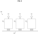
- Figure 5 schematically depicts an electron-optical device array 299.
- the assessment apparatus 100 of Figure 1 comprises the electron-optical device array 299 instead of the electron-optical apparatus 140.
- Such an electron-optical device array 299 is also referred to as a multi-column array.
- the different columns (or electron-optical devices 230) may comprise in use a plurality of beams such as a beam grid.
- the electron-optical device array 299 comprises a plurality of electron-optical devices 230 of the type shown in Figure 2 .
- one or more electron-optical elements may be shared between more than one of the electron-optical devices 230 of the electron-optical device array 299.
- the electron-optical elements may comprise one or more plates 261 in which a plurality of beam apertures 266 are defined for respective beam paths.
- one or more sources 201 may be shared between more than one of the electron-optical devices 230 of the electron-optical device array 299.
- the sources may be comprised in a source array having different sources generating a source beam for different respective electron-optical device 230.
- Each electron-optical device 230 of the electron-optical device array 299 may be configured in any of the ways described herein.
- the disclosure in WO 2022008286 A1 of how the objective lens is incorporated and adapted for use in the multi-device arrangement is hereby incorporated by reference.
- the disclosure in WO 2021165135 A1 of a multi-device arrangement of a multi-beam device comprising a collimator at, or proximate to, an intermediate focus is hereby incorporated by reference.
- FIG. 6 schematically depicts an electron-optical apparatus 140 of an assessment apparatus, e.g. the assessment apparatus 100 of Figure 1 .
- the electron-optical apparatus 140 comprises an electron-optical device 230.
- the field of view of the electron-optical device 230 may be, for example, of the order of 100s of microns across the primary beams 211, 212, 213 at the sample 208.
- the electron-optical apparatus 140 of Figure 6 may be the electron-optical apparatus 140 of Figure 2 in which the electron-optical device 230 comprises a Coulomb aperture array 272, a macro condenser lens 274, a source converter (or micro-optical array) 220 and an objective lens 243.
- the electron-optical apparatus 140 defines an electron-optical axis 204.
- the Coulomb aperture array 272 may be referred to as a beam former array.
- the source 201 generates a source beam 202.
- the Coulomb aperture array 272 defines a plurality of primary beams 211, 212, 213 from the source beam 202.
- the Coulomb aperture array 272, in operation, is configured to block off peripheral electrons to reduce electron-electron interactions (also referred to as Coulomb interactions) that may generate aberrations.
- the macro condenser lens 274 is configured to at least partly collimate the primary beams 211, 212, 213. In an embodiment the macro condenser lens 274 is magnetic. The macro condenser lens 274 may be a non-rotational condenser lens. In an embodiment the macro condenser lens 274 is configured to operate on a plurality of, optionally all of, the primary beams 211, 212, 213.
- the source converter 220 is configured to convert the primary beams 211, 212, 213 transmitted by the Coulomb aperture array 272 into the beams that are directed towards the sample 208.
- the source converter 220 is a module.
- the source converter 220 may comprise a plurality of separate electron-optical elements.
- the source converter 220 comprises a beam limiting aperture array 252 with an aperture pattern (i.e. apertures arranged in a formation) configured to define the outer dimensions of the primary beams 211, 212, 213 directed towards the sample 208.
- the beam limiting aperture array 252 may be a plate 261.
- the beam limiting aperture array 252 defines a plurality of beams from each of the primary beams 211, 212, 213 directed to the beam limiting aperture array 252.
- the beam limiting aperture array 252 maintains the number of the primary beams 211, 212, 213 incident on the beam limiting aperture array 252.
- the source converter 220 may comprise a corrector array such as an aberration reduction array 224 configured to reduce aberrations of the primary beams 211, 212, 213.
- the aberration reduction array 224 comprises a plurality of lenses configured to operate on respective primary beams 211, 212, 213.
- the aberration reduction array 224 may, for example, comprise a field curvature compensator array (not shown) comprising lenses.
- the aberration reduction array 224 may comprise an astigmatism compensator array (not shown) comprising stigmators.
- the stigmators may, for example, be controlled to operate on the primary beams 211, 212, 213 to reduce astigmatism aberrations.
- the source converter 220 may comprise a deflector array 295 comprising deflectors 295_1, 295_2, 295_3 for the beam paths of respective primary beams 211, 212, 213.
- the deflectors 295_1, 295_2, 295_3 are configured to deflect the beam paths of the primary beams 211, 212, 213 towards the front focal plane of the objective lens 243 to ensure that the individual primary beams 211, 212, 213 will impinge on the sample 208 substantially perpendicular.
- the objective lens 243 is magnetic. In an embodiment the objective lens 243 is a macroscopic lens configured to manipulate a plurality of, optionally all of, the primary beams 211, 212, 213 simultaneously. The objective lens 243 focuses the primary beams 211, 212, 213 onto the surface of the sample 208. The primary beams 211, 212, 213 form respective probe spots 281, 282, 283 on the surface of the sample 208.
- the deflectors 295_1, 295_2, 295_3 of the deflector array 295 deflect the individual primary beams 211, 212, 213 to the front focal plane of the objective lens to ensure that the individual primary beams 211, 212, 213, in use, impinge on the substrate 208 substantially perpendicular.
- the objective lens 243 is a macroscopic lens containing both magnetic and electrostatic lenses. In such an embodiment the macroscopic electrostatic lenses manipulate the plurality of the primary beams 211, 212, 213 simultaneously.
- the objective lens 243 comprises one or more scan deflectors (electrostatic and/or magnetic) to scan the plurality of primary beams 211, 212, 213 over the substrate 208.
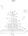
- Figure 7 schematically depicts an electron-optical apparatus 140 of an assessment apparatus, e.g. the assessment apparatus 100 of Figure 1 .
- the electron-optical apparatus 140 comprises an electron-optical device 230 that comprises a beam limit aperture 125 (the image actually shows an array of selectable beam limiting apertures), a condenser lens 126, a column aperture 135 (again indicated as an array of selectable column apertures 135), an objective lens 243 and a detector array 240.
- the source 201 is configured to generate a source beam 202.
- a gun aperture 124 blocks peripheral electrons of the source beam 202.
- the source beam 202 passes through the beam limit aperture 125, the condenser lens 126 and the column aperture 135.
- the condenser lens 126 may be magnetic, electrostatic or a combination of magnetic and electrostatic.
- the electron-optical device 230 comprises electromagnetic multipole, e.g. quadrupole, electron lenses.
- the electron-optical device 230 may comprise a first multipole lens 148 and a second multipole lens 158.
- the first multipole lens 148 and the second multipole lens 158 are used for controlling the source beam 202.
- the first multipole lens 148 may be configured to adjust the beam current of the source beam 202.
- the second multipole lens 158 may be configured to adjust the size of the probe spot 281 and/or the shape of the source beam 202.
- the objective lens 243 focuses the source beam 202 onto the sample 208.
- the objective lens 243 comprises a pole piece 132a, a control electrode 132b, a deflector 132c and an exciting coil 132d.
- a deflector such as the deflector 132c or other deflectors in the objective lens 243 are configured to scan the source beam 202 across the surface of the sample 208.
- the detector array 240 is configured to detect signal electrons from the sample 208.
- FIG 8 schematically depicts an electron-optical apparatus 140 of an assessment apparatus, e.g. the assessment apparatus 100 of Figure 1 .
- the electron-optical apparatus 140 may be the electron-optical apparatus 140 of Figure 2 in which the electron-optical device 230 comprises a condenser lens array 231, a macro collimator 270, the detector array 240, a deflector array 295 and an objective lens array 241.
- the source 201, the condenser lens array 231, the objective lens array 241 and the sample 208 may be as described above.
- the source is configured to generate a source beam 202.
- the condenser lens array 231 is configured to define a plurality of primary beams 211, 212, 213 from the source beam 202.
- the disclosure in EP1602121A1 of a lens array to split a beam into a plurality of beams, with the lens array providing a lens for each beam, is hereby incorporated by reference as a possible implementation of the condenser lens array 231.
- the condenser lens array 231 comprises three plates 261 configured as an Einzel lens.
- An Einzel lens is configured to substantially ensure that the energy of an electron leaving the lens is the same as when the electron arrived at the lens.
- Such a lens maintains the energy of an electron between arriving and leaving the lens, for example the condenser lenses of the condenser lens array 231.
- dispersion only occurs within the condenser lens array 231 itself, thereby limiting chromatic aberrations.
- the chromatic aberrations caused by this condenser lens array 231 is limited, e.g. having a negligible effect.
- the detector array 240 is configured to detect signal electrons by reference to the energy of the signal electron.
- scintillators e.g. YAG do not directly detect electrons but generate light which is then detected.
- the signal electrons emitted from the sample 208 gain energy from the electromagnetic fields between the detector array 240 and the sample 208.
- the objective lens array 241 is located between the detector array 240 and the sample 208.
- the photon transport unit comprises an array of optical fibers 298.
- Each optical fiber 298 comprises an end which is arranged adjacent or attached to one of the fluorescent strips 292 for coupling photons from the fluorescent strip 292 into the optical fiber 298, and another end which is arranged to project photons from the optical fiber 298 onto the photo detector.
- the optical to electrical converter or photo diode is located immediately adjacent the electron to light converter, avoiding the need for optical fibers.
- Figure 10 is a bottom view of the detector array 240 which comprises a detector substrate 264 on which are provided a plurality of detector elements 265 each surrounding a beam aperture 266.
- the detector array 240 may be provided at a downbeam surface of a plate 261 comprising beam apertures 266.
- the detector elements 265 are charge capture electrodes, for example metal plates.
- the beam apertures 266 may be formed by etching through the detector substrate 264. In the arrangement shown in Figure 10 , the beam apertures 266 are in a hexagonal close packed array.
- the beam apertures 266 can also be differently arranged, e.g. in a rectangular array.
- the controller 150 is configured to control the electron-optical device 230.
- the controller 150 may be configured to control potentials applied to electrodes of lenses of the electron-optical device 230.
- the controller 150 is configured to control the actuatable stage 209 to move the sample 208 during inspection of the sample 208.
- the controller 150 may enable the actuatable stage 209 to move the sample 208 in a direction, for example continuously, such as at a constant speed, at least during sample inspection, which may be referred to as a type of scanning.
- the speed of the actuatable stage 209 may be referred to as the moving rate.
- the controller 150 may control movement of the actuatable stage 209 so as to change the speed of movement of the sample 208 relative to the beam paths dependent on one or more parameters.
- the controller 150 may control deflection of scan deflectors so that the beam paths move relative to the actuatable stage 209 and thus over the surface of the sample 208.
- the controller 150 may change a beam deflection of a scan deflector and thus the scanning of the primary beams 211, 212, 213 over the sample 208 dependent on one or more parameters.
- the controller 150 may control a scan deflector and/or the speed of the actuatable stage 209 and/or the direction of movement of the actuatable stage 209 depending on characteristics of the assessment process.
- the disclosure in EP4086933 A1 of a combined stepping and scanning strategy of the stage and scanning deflectors is hereby incorporated by reference.
- the moving rate may at different times comprise a stepping frequency and/or a stage scanning rate.
- the primary beams 211, 212, 213 may be susceptible to interference by nearby voltage sources, particularly high-voltage sources.
- Example sources of interference include interferometers and various sensors.
- components of the electron-optical device 230 are maintained at a large negative voltage.
- external components that are at (absolute) ground potential may also be sources of interference.
- the electron-optical device 230 may comprise a voltage shield (not shown) configured to shield the primary beams 211, 212, 213 from such interferences.
- the voltage shield may generally be in the form of a plate.
- the voltage shield may comprise an electrically conductive material, such as a metallic material.
- the voltage shield may extend laterally from the electron-optical device 230, and may extend far enough to provide voltage shielding over the full extent and the full movable range of the actuatable stage 209. As such, the lateral extent of the voltage shield may be substantially greater than the lateral footprint of the electron-optical device 230.
- the voltage shield may be divided into an inner part and an outer part (not shown).
- the inner part may be rigidly attached to the electron-optical device 230.
- the outer part surrounding the inner part and attached to the casing of the electron-optical apparatus 140, such as via flexible supports.
- the inner part may have a lateral extent not much larger than the electron-optical device 230, so that it can be extracted together with the electron-optical device 230 relatively easily.
- a gap may exist between the inner and outer parts of the voltage shield.
- the gap may surround the inner part.
- the gap may be shaped so as to maintain continuity of the voltage shield. That is, notwithstanding the existence of the gap, the voltage shield may be shaped to prevent external electric fields from leaking through the gap.
- the inner and outer parts of the voltage shield may be shaped to maintain a lateral overlap along the gap. There may be enough lateral overlap to accommodate relative movements between the inner and outer parts of the voltage shield resulting from mechanical vibrations. That is, the lateral overlap may be large enough so that the continuity of the voltage shield is maintained even when the relative movements between the inner and outer parts of the voltage shield are at a maximum amplitude.
- a straightforward implementation may be to connect the inner and outer parts of the voltage shield using a flexible electric cable (not shown).
- a flexible electric cable may be difficult to access. Without disconnecting the cable, it may not be possible to extract the electron-optical device 230 from the electron-optical apparatus 140. Therefore, using a flexible electric cable has disadvantages.
- an electrical connection system that operates automatically.
- the term "passively" may mean that the electrical connection system is able operate without requiring an electrical supply, or without relying on electrical sensors or electro-mechanical actuators.
- Such an electrical connection system may be useful for implementing the voltage shield.
- the electrical connection system may be used in various other technical applications, including those unrelated to lithography, where a passive and automatic electrical connection is beneficial.
- the electrical connection system may take advantage of changes in a fluid pressure in the environment surrounding the electrical connection system.
- the term "fluid” encompasses liquids, gasses and/or plasmas.
- the voltage shield may be in a relative vacuum (i.e. below atmospheric pressure) environment during normal operation of the electron-optical apparatus 140, and may be in an atmospheric-pressure environment during maintenance of the electron-optical apparatus 140.
- the electrical connection system may operate in response to this change in pressure.
- the pressure change may be between atmospheric pressure and a positive pressure greater than atmospheric pressure.
- the electrical connection system may accordingly operate in response to changes between atmospheric and positive pressures. More generally, the electrical connection system may operate in response to pressure changes, irrespective of whether the pressures are positive, negative, or close to atmospheric.
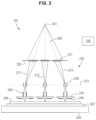
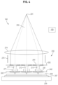
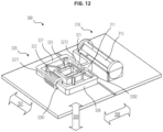
- the electrical connection system 300 may comprise: a first body 310; a first electrical contact member 311 attached to the first body 310; a second body 320 movable relative to the first body 310; and a second electrical contact member 321 attached to the second body 320.
- the first and second bodies 310, 320 may be separated by a gap, so that they are not in rigid mechanical contact.
- the first and second bodies 310, 320 may move relative to each other due to mechanical vibrations. Such movements may typically be about 1 mm in amplitude in most directions, but may be as much as 4 mm in some applications.
- the electrical connection system 300 may further comprise a pneumatic actuator 322.
- the pneumatic actuator 322 may be a passive component.
- the pneumatic actuator 322 may be configured to change length in a first direction 307.
- the pneumatic actuator 322 may change length in response to changes in the fluid pressure surrounding the pneumatic actuator 322.
- the electrical connection system 300 may have a disconnected state and a connected state.
- the pneumatic actuator 322 in the disconnected state, may have a first length whereby the first and second electrical contact members 311, 321 are not in electrical contact.
- the pneumatic actuator 322 in a connected state, may have a second length whereby the first and second electrical contact members 311, 321 are in electrical contact.
- the electrical connection system 300 may further comprise a first compliant member 315 through which the first electrical contact member 311 is attached to the first body 310.
- the first compliant member 315 may configured to accommodate relative movements between the first and second bodies 310, 320 in one or more directions. For example, as shown in Figures 14B and 14C , the first compliant member 315 may accommodate relative movements between the first and second bodies 310, 320 in a second direction 308, 309 different from the first direction 307 (note that the relative movement in the direction 309 as shown in Figure 14C is visually small, but clearly observable by comparison with Figure 12 ). It should be understood that the first compliant member 315 may also accommodate relative movements in the first direction 307, i.e. the direction in which the pneumatic actuator 322 is configured to change length.
- the electrical connection system 300 may transition between the connected state and the disconnected state passively and automatically.
- the electrical connection system 300 may be configured to shift from the connected state to the disconnected state when the fluid pressure rises above a threshold. Additionally or alternatively, the electrical connection system 300 may be configured to shift from the disconnected state to the connected state when the fluid pressure falls below a threshold. It should be noted that the threshold for shifting from the connected state to the disconnected state may be the same or different from the threshold for shifting from the disconnected state to the connected state. That is, an amount of hysteresis may exist, which may be by design or due to material properties, friction, and the like.
- the threshold When the electrical connection system 300 is configured for a vacuum enclosure, such as in the electron-optical apparatus 140, the threshold may be set at a value somewhere between atmospheric pressure and the vacuum pressure used during normal operation. In particular, as may be the case for the electron-optical apparatus 140, an electrical connection may always be required during normal operation, and a disconnection may always be required during maintenance. Therefore, by configuring the pressure threshold accordingly, the electrical connection system 300 may always be in the required state (i.e. disconnected or connected).
- the first and second electrical contact members 311, 321 can sometimes become welded together, for example due to large transient currents and arcing.
- the pneumatic actuator 322 may be sized to generate enough force to break any welded spots, so as to shift the electrical connection system 300 from the connected state to the disconnected state.
- the pneumatic actuator 322 may be configured to increase in length in response to a decreasing fluid pressure. That is, as the fluid pressure decreases, the gas or gas mixture inside the pneumatic actuator 322 may expand and cause the increase in length. Conversely, the pneumatic actuator 322 may be configured to decrease in length in response to an increasing fluid pressure.
- the pneumatic actuator 322 may be configured to decrease in length in response to a decreasing fluid pressure, and/or the pneumatic actuator 322 may be configured to increase in length in response to an increasing fluid pressure.
- This configuration may be useful, for example, for when a disconnection is required when the apparatus is under vacuum and a connection is required when the apparatus is at atmospheric pressure.
- This configuration may also be useful for apparatuses that normally operate at a positive pressure, and which return to atmospheric pressure for maintenance.
- first direction 307 and the second direction 308, 309 may be orthogonal to each other. It should be understood, however, that the first direction 307 and the second direction 308, 309 need not necessarily be orthogonal to each other; they may generally be non-parallel to each other.
- the first compliant member 315 may serve to accommodate relative movements in more than one direction.
- the first compliant member 315 may be further configured to accommodate relative movements between the first and second bodies 310, 320 in a third direction 309 different from each of the first direction 307 and the second direction 308.
- the third direction 309 may be orthogonal to each of the first and second directions 307, 308.
- the first, second and third directions 307, 308, 309 need not necessarily be orthogonal to one another; they may generally be mutually non-parallel to one another. More particularly, the first, second and third directions 307, 308, 309 may not be on the same plane.
- the electrical connection system 300 may further comprise a second compliant member 325. As shown in Figure 14A , the second compliant member 325 may be configured to accommodate relative movements between the first and second bodies 310, 320 in the first direction 307.
- the electrical connection system 300 may accommodate relative movements between the first body 310 and the second body 320 with three linear degrees of freedom, all the while maintaining the connected state when required, and automatically and passively shifting to the disconnected state in response to an appropriate pressure change.
- the first and/or second compliant members 315, 325 may be variously implemented. For example, as shown in Figures 12 to 14C , they may be implemented using one or more leaf springs. Alternatively, they may be implemented using one or more helical or torsional springs. As yet another alternative, they may be implemented using a resilient material such as rubber or foam. A mixture or combination of the aforesaid may also be used.
- the electrical connection system 300 may additionally accommodate relative rotational movements between the first body 310 and the second body 320 with one, two or three degrees of rotational freedom. Therefore, in sum, the electrical connection system 300 may accommodate relative movements with up to six degrees of freedom as required.
- the first and/or second compliant members 315, 325 may be configured especially to accommodate rotational relative movements. Alternatively, the inherent flexibility in the material from which the first and/or second compliant members 315, 325 are constructed may provide the requisite amount of accommodation of rotational relative movements.
- first and/or second compliant members 315, 325 may be useful for accommodating relative movements between the first and second bodies 310, 320, it may be desirable to ensure that there are no unconstrained internal degrees of freedom.
- an unconstrained degree of freedom may arise when both the first and second compliant members 315, 325 have significant compliance in a common direction.
- the existence of an unconstrained degree of freedom may allow certain parts to vibrate, or even resonate. Therefore, it may be desirable for relative movements in each of the first, second and third directions 307, 308, 309 to be accommodated substantially exclusively by one, and not both, of the first and second compliant members 315, 325.
- the second compliant member 325 may be more rigid than the first compliant member 315 in the third direction 309, the third direction 309 being different from (but not necessarily orthogonal to) each of the first direction 307 and the second direction 308. Therefore, relative movements in the third direction 309 may be accommodated substantially exclusively by the second compliant member 325.
- the first and second compliant members 315, 325 may be provided anywhere within the electrical connection system 300 as long as they are capable of performing their respective functions.
- the second compliant member 325 may be attached to the second body 320.
- the first compliant member 315 may be attached to the first body 310.
- the second compliant member 325 may be provided to accommodate relative movements between the first and second bodies 310, 320 in the first direction 307.
- the pneumatic actuator 322 it is possible exploit the compliance of the pneumatic actuator 322, so that it additionally serves as the second compliant member 325. That is, in Figure 15 , for example, the item shown as the second compliant member 325 may be replaced by a rigid attachment, and the pneumatic actuator 322, by virtue of its compliance, may perform the same function as the second compliant member 325 as shown.
- the pneumatic actuator 322 may be variously implemented.
- the pneumatic actuator 322 may comprise a sealed internal volume, wherein a change in the volume causes the pneumatic actuator 322 to change length.
- the pneumatic actuator 322 may comprise a bellows, and the sealed internal volume is the internal volume of the bellows.
- the bellows may be constructed out of metal, for example stainless steel. Compared with other implementations, the use of a bellows may avoid creating a sliding electrical contact. Sliding contacts may be undesirable because they may cause abrasion and generate contaminant particles.
- a bellows refers to a single item.
- the amount of gas present in the pneumatic actuator 322 can be varied as required, as long as the pneumatic actuator 322 is capable of changing length in response to fluid pressure changes relevant for the particular technical application.
- the sealed internal volume may be filled with a gas or gas mixture at atmospheric pressure.
- the term "unstressed state” refers to a state in which the mechanical forces in the pneumatic actuator 322 in isolation are in equilibrium, and the pressures inside and outside of the pneumatic actuator 322 are equal. While in the unstressed state, internal mechanical stresses may nevertheless exist in the construction material of the pneumatic actuator 322. It should also be noted that substantially no gas (i.e. substantially perfect vacuum) is present in the internal volume of the pneumatic actuator 322 (the pneumatic actuator 322 would still be able to change length given appropriate surrounding fluid pressures).
- the pneumatic actuator 322 may be provided anywhere within the electrical connection system 300 as long as it is capable of performing its intended function. For example, as shown in Figures 12 to 15 , the pneumatic actuator 322 may be attached to the second body 320.
- the pneumatic actuator 322 by changing length, may cause the transition between the connected state and the disconnected state through various means.
- the pneumatic actuator 322 may act indirectly.
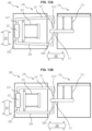
- the electrical connection system 300 may further comprise a lever 327, wherein the pneumatic actuator 322 is configured to act through a first end 3271 of the lever 327.
- the lever 327 may be rotatably attached to the second body 320.
- the lever 327 may be attached to the second body 320 through the second compliant member 325.
- the lever 327 may be integrally formed with the second compliant member 325, and may be able to rotate due to the compliance of the second compliant member 325.
- the lever 327 may be rotatable about a virtual pivot point.
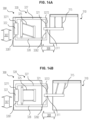
- an increase in length of the pneumatic actuator 322 may result in a decrease in distance between the second end 3272 of the first lever 327 and the second end 3272 of the second lever 328.
- the first and second levers 327, 328 may form a clamp configured to clamp onto the first electrical contact member 311 in the connected state.
- the clamping force may be sufficient to maintain a reliable electrical connection.
- the bellows may have a cross-sectional area of about 1 cm 2 , and the contact force may be about 5 N to 9 N.
- a decrease in length of the pneumatic actuator 322 may result in an increase in distance between the second end 3272 of the first lever 327 and the second end 3272 of the second lever 328. This may provide a force sufficient to break any weld that may have formed between the first electrical contact member 311 and the second electrical contact member 321.
- the forces acting on the first electrical contact member 311 may be symmetrical (that is, equal and opposite), so that the first electrical contact member 311 is not biased towards one side.
- a single pneumatic actuator 322 may be required for implement the actuation.
- first and second levers 327, 328 may be electrically conductive. Therefore, one or both of the first and second levers 327, 328 may serve as part of the electrically conductive path.
- first and second levers 327, 328 may be non-conductive, and a separate electrical conductor (e.g. a cable) may be provided to complete the conductive path from the second electrical contact member 321.
- an additional electrical contact member may be provided on the second end 3282 of the second lever 328.
- the pneumatic actuator 322 may have a stationary end 3221 which is rigidly attached to the second body 320.
- the pneumatic actuator 322 may have an actuation end which is movable relative to the stationary end 3221, thereby allowing the pneumatic actuator 322 to change length.
- the pneumatic actuator 322 may act directly.
- the second electrical contact member 321 may be provided on, or integrally formed with, the actuation end 3222 of the pneumatic actuator 322.
- the electrical connection system 300 may further comprise a second pneumatic actuator 323 attached to the second body 320.
- the first and second pneumatic actuators 322, 323 may be positioned to actuate in opposite directions.
- the first electrical contact member 311 may be positionable between the first and second pneumatic actuators 322, 323.
- the first and second pneumatic actuators 322, 323 may exert substantially equal and opposite forces on the first electrical contact member 311 when in the connected state. This may prevent biasing the 311 towards one side.
- One or both of the first and second pneumatic actuators 322, 323 may be electrically conductive. As a result, the one or both of the first and second pneumatic actuators 322, 323 may form part of the electrically conductive path. Alternatively, one or both of the first and second pneumatic actuators 322, 323 may be non-conductive, and a separate electrical conductor may be provided to complete the conductive path from the second electrical contact member 321.
- the first and second bodies 310, 320 may be the voltage shielding plates mentioned above.
- the first and second bodies 310, 320 may be laterally overlapped so as to form a voltage shield.
- the voltage shield may be continuous.
- the first and second bodies 310, 320 may be separated by a gap so as to allow relative movement.
- the charged particle-optical apparatus may comprise the electrical connection system 300.
- Embodiments of the invention may form part of a mask inspection apparatus, a metrology apparatus, or any apparatus that measures or processes an object such as a wafer (or other substrate) or mask (or other patterning device).
- embodiments of the invention may be implemented in hardware, firmware, software, or any combination thereof. Embodiments of the invention may also be implemented as instructions stored on a machine-readable medium, which may be read and executed by one or more processors.
- a machine-readable medium may include any mechanism for storing or transmitting information in a form readable by a machine (e.g., a computing device).
- a machine-readable medium may include read only memory (ROM); random access memory (RAM); magnetic storage media; optical storage media; flash memory devices; electrical, optical, acoustical or other forms of propagated signals (e.g. carrier waves, infrared signals, digital signals, etc.), and others.
- firmware, software, routines, instructions may be described herein as performing certain actions.
Landscapes
- Physics & Mathematics (AREA)
- Fluid Mechanics (AREA)
- Coupling Device And Connection With Printed Circuit (AREA)
- Analysing Materials By The Use Of Radiation (AREA)
Priority Applications (1)
| Application Number | Priority Date | Filing Date | Title |
|---|---|---|---|
| EP25174125.2A EP4576149A3 (de) | 2025-05-02 | 2025-05-02 | Elektrisches verbindungssystem |
Applications Claiming Priority (1)
| Application Number | Priority Date | Filing Date | Title |
|---|---|---|---|
| EP25174125.2A EP4576149A3 (de) | 2025-05-02 | 2025-05-02 | Elektrisches verbindungssystem |
Publications (2)
| Publication Number | Publication Date |
|---|---|
| EP4576149A2 true EP4576149A2 (de) | 2025-06-25 |
| EP4576149A3 EP4576149A3 (de) | 2025-11-19 |
Family
ID=95519276
Family Applications (1)
| Application Number | Title | Priority Date | Filing Date |
|---|---|---|---|
| EP25174125.2A Pending EP4576149A3 (de) | 2025-05-02 | 2025-05-02 | Elektrisches verbindungssystem |
Country Status (1)
| Country | Link |
|---|---|
| EP (1) | EP4576149A3 (de) |
Citations (11)
| Publication number | Priority date | Publication date | Assignee | Title |
|---|---|---|---|---|
| WO2004081910A2 (en) | 2003-03-10 | 2004-09-23 | Mapper Lithography Ip B.V. | Apparatus for generating a plurality of beamlets |
| WO2012165955A2 (en) | 2011-05-30 | 2012-12-06 | Mapper Lithography Ip B.V. | Charged particle multi-beamlet apparatus |
| WO2021156121A1 (en) | 2020-02-07 | 2021-08-12 | Asml Netherlands B.V. | Charged particle manipulator device |
| EP3869535A1 (de) | 2020-02-21 | 2021-08-25 | ASML Netherlands B.V. | Beurteilungswerkzeug für geladene partikel, inspektionsverfahren |
| WO2021165135A1 (en) | 2020-02-21 | 2021-08-26 | Asml Netherlands B.V. | Inspection apparatus |
| WO2021165136A1 (en) | 2020-02-21 | 2021-08-26 | Asml Netherlands B.V. | Charged particle inspection tool, inspection method |
| WO2021204734A1 (en) | 2020-04-06 | 2021-10-14 | Asml Netherlands B.V. | Charged particle assessment tool, inspection method |
| WO2022008286A1 (en) | 2020-07-06 | 2022-01-13 | Asml Netherlands B.V. | Charged-particle multi-beam column, charged-particle multi-beam column array, inspection method |
| WO2022058252A1 (en) | 2020-09-17 | 2022-03-24 | Asml Netherlands B.V. | Objective lens array assembly, electron-optical system, electron-optical system array, method of focusing, objective lens arrangement |
| WO2022101072A1 (en) | 2020-11-12 | 2022-05-19 | Asml Netherlands B.V. | Objective lens array assembly, electron-optical system, electron-optical system array, method of focusing |
| EP4086933A1 (de) | 2021-05-03 | 2022-11-09 | ASML Netherlands B.V. | System für geladene teilchen, verfahren zur bearbeitung einer probe unter verwendung eines mehrfachstrahls von geladenen teilchen |
Family Cites Families (3)
| Publication number | Priority date | Publication date | Assignee | Title |
|---|---|---|---|---|
| GB1373680A (en) * | 1973-02-16 | 1974-11-13 | Atomic Energy Authority Uk | Electrical apparatus |
| DE3714007A1 (de) * | 1987-04-27 | 1988-11-10 | Vdo Schindling | Druckfuehler und verfahren zur herstellung |
| EP4290550A1 (de) * | 2022-06-10 | 2023-12-13 | ASML Netherlands B.V. | Elektronenoptische vorrichtung |
-
2025
- 2025-05-02 EP EP25174125.2A patent/EP4576149A3/de active Pending
Patent Citations (12)
| Publication number | Priority date | Publication date | Assignee | Title |
|---|---|---|---|---|
| WO2004081910A2 (en) | 2003-03-10 | 2004-09-23 | Mapper Lithography Ip B.V. | Apparatus for generating a plurality of beamlets |
| EP1602121A2 (de) | 2003-03-10 | 2005-12-07 | Mapper Lithography Ip B.V. | Vorrichtung zur erzeugung einer vielzahl von teilstrahlen |
| WO2012165955A2 (en) | 2011-05-30 | 2012-12-06 | Mapper Lithography Ip B.V. | Charged particle multi-beamlet apparatus |
| WO2021156121A1 (en) | 2020-02-07 | 2021-08-12 | Asml Netherlands B.V. | Charged particle manipulator device |
| EP3869535A1 (de) | 2020-02-21 | 2021-08-25 | ASML Netherlands B.V. | Beurteilungswerkzeug für geladene partikel, inspektionsverfahren |
| WO2021165135A1 (en) | 2020-02-21 | 2021-08-26 | Asml Netherlands B.V. | Inspection apparatus |
| WO2021165136A1 (en) | 2020-02-21 | 2021-08-26 | Asml Netherlands B.V. | Charged particle inspection tool, inspection method |
| WO2021204734A1 (en) | 2020-04-06 | 2021-10-14 | Asml Netherlands B.V. | Charged particle assessment tool, inspection method |
| WO2022008286A1 (en) | 2020-07-06 | 2022-01-13 | Asml Netherlands B.V. | Charged-particle multi-beam column, charged-particle multi-beam column array, inspection method |
| WO2022058252A1 (en) | 2020-09-17 | 2022-03-24 | Asml Netherlands B.V. | Objective lens array assembly, electron-optical system, electron-optical system array, method of focusing, objective lens arrangement |
| WO2022101072A1 (en) | 2020-11-12 | 2022-05-19 | Asml Netherlands B.V. | Objective lens array assembly, electron-optical system, electron-optical system array, method of focusing |
| EP4086933A1 (de) | 2021-05-03 | 2022-11-09 | ASML Netherlands B.V. | System für geladene teilchen, verfahren zur bearbeitung einer probe unter verwendung eines mehrfachstrahls von geladenen teilchen |
Also Published As
| Publication number | Publication date |
|---|---|
| EP4576149A3 (de) | 2025-11-19 |
Similar Documents
| Publication | Publication Date | Title |
|---|---|---|
| US11961697B2 (en) | Apparatus using charged particle beams | |
| US12030772B2 (en) | MEMS image forming element with built-in voltage generator | |
| US20240242921A1 (en) | Charged particle apparatus and method | |
| US20230352266A1 (en) | Electron-optical device | |
| US20240128043A1 (en) | Charged particle apparatus and method | |
| US20240136147A1 (en) | Charged particle-optical device, charged particle apparatus and method | |
| US20250014855A1 (en) | Charged particle apparatus and method | |
| US20250095950A1 (en) | Electron-optical device | |
| WO2022238137A1 (en) | Assessment system, method of assessing | |
| EP4576149A2 (de) | Elektrisches verbindungssystem | |
| US20240038485A1 (en) | Electron-optical device | |
| WO2022058253A2 (en) | Charged particle assessment tool, inspection method | |
| EP4354486A1 (de) | Elektronenoptisches element | |
| EP4439621A1 (de) | Abschirmanordnung für ein elektronenoptisches modul | |
| US20250357070A1 (en) | Electron-optical assembly | |
| EP4391006A1 (de) | Vorrichtung für geladene teilchen, verfahren zur projektion geladener teilchen, verfahren zur beurteilung einer probe | |
| EP4020517A1 (de) | Elektronenoptische vorrichtung | |
| EP4418302A1 (de) | Optisches element für geladene teilchen, optisches modul für geladene teilchen, beurteilungsvorrichtung, chipanordnung, verfahren zur herstellung | |
| EP4307335A1 (de) | Isolierender abstandshalter für elektronenoptische anordnung | |
| WO2024133468A1 (en) | Charged particle apparatus, method of projecting charged particles, method of assessing a sample | |
| EP4352774A1 (de) | Verfahren zur kompensation eines effekts einer elektrodenverzerrung, bewertungssystem |
Legal Events
| Date | Code | Title | Description |
|---|---|---|---|
| PUAI | Public reference made under article 153(3) epc to a published international application that has entered the european phase |
Free format text: ORIGINAL CODE: 0009012 |
|
| STAA | Information on the status of an ep patent application or granted ep patent |
Free format text: STATUS: THE APPLICATION HAS BEEN PUBLISHED |
|
| AK | Designated contracting states |
Kind code of ref document: A2 Designated state(s): AL AT BE BG CH CY CZ DE DK EE ES FI FR GB GR HR HU IE IS IT LI LT LU LV MC ME MK MT NL NO PL PT RO RS SE SI SK SM TR |
|
| PUAL | Search report despatched |
Free format text: ORIGINAL CODE: 0009013 |
|
| AK | Designated contracting states |
Kind code of ref document: A3 Designated state(s): AL AT BE BG CH CY CZ DE DK EE ES FI FR GB GR HR HU IE IS IT LI LT LU LV MC ME MK MT NL NO PL PT RO RS SE SI SK SM TR |
|
| RIC1 | Information provided on ipc code assigned before grant |
Ipc: H01H 35/32 20060101AFI20251013BHEP Ipc: H01J 37/04 20060101ALI20251013BHEP Ipc: H01H 1/32 20060101ALN20251013BHEP |