EP4575772A1 - Elektronische vorrichtung mit neuronaler verarbeitungseinheit und betriebsverfahren dafür - Google Patents
Elektronische vorrichtung mit neuronaler verarbeitungseinheit und betriebsverfahren dafür Download PDFInfo
- Publication number
- EP4575772A1 EP4575772A1 EP23865910.6A EP23865910A EP4575772A1 EP 4575772 A1 EP4575772 A1 EP 4575772A1 EP 23865910 A EP23865910 A EP 23865910A EP 4575772 A1 EP4575772 A1 EP 4575772A1
- Authority
- EP
- European Patent Office
- Prior art keywords
- processing unit
- neural network
- computation
- electronic device
- central processing
- Prior art date
- Legal status (The legal status is an assumption and is not a legal conclusion. Google has not performed a legal analysis and makes no representation as to the accuracy of the status listed.)
- Pending
Links
Images


Classifications
-
- G—PHYSICS
- G06—COMPUTING OR CALCULATING; COUNTING
- G06F—ELECTRIC DIGITAL DATA PROCESSING
- G06F8/00—Arrangements for software engineering
- G06F8/40—Transformation of program code
- G06F8/41—Compilation
- G06F8/44—Encoding
-
- G—PHYSICS
- G06—COMPUTING OR CALCULATING; COUNTING
- G06F—ELECTRIC DIGITAL DATA PROCESSING
- G06F13/00—Interconnection of, or transfer of information or other signals between, memories, input/output devices or central processing units
- G06F13/38—Information transfer, e.g. on bus
- G06F13/40—Bus structure
- G06F13/4004—Coupling between buses
- G06F13/4027—Coupling between buses using bus bridges
- G06F13/4031—Coupling between buses using bus bridges with arbitration
-
- G—PHYSICS
- G06—COMPUTING OR CALCULATING; COUNTING
- G06F—ELECTRIC DIGITAL DATA PROCESSING
- G06F9/00—Arrangements for program control, e.g. control units
- G06F9/06—Arrangements for program control, e.g. control units using stored programs, i.e. using an internal store of processing equipment to receive or retain programs
- G06F9/30—Arrangements for executing machine instructions, e.g. instruction decode
- G06F9/38—Concurrent instruction execution, e.g. pipeline or look ahead
- G06F9/3877—Concurrent instruction execution, e.g. pipeline or look ahead using a slave processor, e.g. coprocessor
-
- G—PHYSICS
- G06—COMPUTING OR CALCULATING; COUNTING
- G06F—ELECTRIC DIGITAL DATA PROCESSING
- G06F9/00—Arrangements for program control, e.g. control units
- G06F9/06—Arrangements for program control, e.g. control units using stored programs, i.e. using an internal store of processing equipment to receive or retain programs
- G06F9/44—Arrangements for executing specific programs
- G06F9/445—Program loading or initiating
- G06F9/44505—Configuring for program initiating, e.g. using registry, configuration files
-
- G—PHYSICS
- G06—COMPUTING OR CALCULATING; COUNTING
- G06F—ELECTRIC DIGITAL DATA PROCESSING
- G06F9/00—Arrangements for program control, e.g. control units
- G06F9/06—Arrangements for program control, e.g. control units using stored programs, i.e. using an internal store of processing equipment to receive or retain programs
- G06F9/46—Multiprogramming arrangements
- G06F9/48—Program initiating; Program switching, e.g. by interrupt
- G06F9/4806—Task transfer initiation or dispatching
- G06F9/4812—Task transfer initiation or dispatching by interrupt, e.g. masked
-
- G—PHYSICS
- G06—COMPUTING OR CALCULATING; COUNTING
- G06F—ELECTRIC DIGITAL DATA PROCESSING
- G06F9/00—Arrangements for program control, e.g. control units
- G06F9/06—Arrangements for program control, e.g. control units using stored programs, i.e. using an internal store of processing equipment to receive or retain programs
- G06F9/46—Multiprogramming arrangements
- G06F9/50—Allocation of resources, e.g. of the central processing unit [CPU]
-
- G—PHYSICS
- G06—COMPUTING OR CALCULATING; COUNTING
- G06F—ELECTRIC DIGITAL DATA PROCESSING
- G06F9/00—Arrangements for program control, e.g. control units
- G06F9/06—Arrangements for program control, e.g. control units using stored programs, i.e. using an internal store of processing equipment to receive or retain programs
- G06F9/46—Multiprogramming arrangements
- G06F9/54—Interprogram communication
- G06F9/544—Buffers; Shared memory; Pipes
-
- G—PHYSICS
- G06—COMPUTING OR CALCULATING; COUNTING
- G06N—COMPUTING ARRANGEMENTS BASED ON SPECIFIC COMPUTATIONAL MODELS
- G06N3/00—Computing arrangements based on biological models
- G06N3/02—Neural networks
- G06N3/04—Architecture, e.g. interconnection topology
- G06N3/045—Combinations of networks
-
- G—PHYSICS
- G06—COMPUTING OR CALCULATING; COUNTING
- G06N—COMPUTING ARRANGEMENTS BASED ON SPECIFIC COMPUTATIONAL MODELS
- G06N3/00—Computing arrangements based on biological models
- G06N3/02—Neural networks
- G06N3/06—Physical realisation, i.e. hardware implementation of neural networks, neurons or parts of neurons
- G06N3/063—Physical realisation, i.e. hardware implementation of neural networks, neurons or parts of neurons using electronic means
-
- G—PHYSICS
- G06—COMPUTING OR CALCULATING; COUNTING
- G06N—COMPUTING ARRANGEMENTS BASED ON SPECIFIC COMPUTATIONAL MODELS
- G06N3/00—Computing arrangements based on biological models
- G06N3/02—Neural networks
- G06N3/08—Learning methods
-
- G—PHYSICS
- G06—COMPUTING OR CALCULATING; COUNTING
- G06F—ELECTRIC DIGITAL DATA PROCESSING
- G06F13/00—Interconnection of, or transfer of information or other signals between, memories, input/output devices or central processing units
- G06F13/14—Handling requests for interconnection or transfer
- G06F13/16—Handling requests for interconnection or transfer for access to memory bus
- G06F13/1605—Handling requests for interconnection or transfer for access to memory bus based on arbitration
- G06F13/161—Handling requests for interconnection or transfer for access to memory bus based on arbitration with latency improvement
-
- G—PHYSICS
- G06—COMPUTING OR CALCULATING; COUNTING
- G06N—COMPUTING ARRANGEMENTS BASED ON SPECIFIC COMPUTATIONAL MODELS
- G06N3/00—Computing arrangements based on biological models
- G06N3/02—Neural networks
- G06N3/10—Interfaces, programming languages or software development kits, e.g. for simulating neural networks
Definitions
- the disclosure relates to an electronic device including a neural processing unit, and an operating method therefor.
- the artificial intelligence technology can be applied to various fields.
- deep learning related to the artificial intelligence technology requires high computing performance, more memory occupancy, and high power consumption for hardware devices and therefore, when the deep learning is applied to mobile terminal applications or data sensor services, a large load can be applied.
- Neural network model technology can reduce energy consumption and inference delay by using a neural network chip (e.g., neural network processing unit (NPU), tensor processing unit (TPU), and field programmable gate array (FPGA)).
- a neural network chip e.g., neural network processing unit (NPU), tensor processing unit (TPU), and field programmable gate array (FPGA)
- NPU neural network processing unit
- TPU tensor processing unit
- FPGA field programmable gate array
- An electronic device can include an application processor (AP).
- An AP chip can have built-in subsystems (e.g., CPU, GPU and NPU) connected by a bus.
- the AP chip or the subsystems inside the AP chip can connect to and communicate with a memory (e.g., dynamic random access memory) outside the AP chip.
- a memory e.g., dynamic random access memory
- a central processing unit and a neural network chip can perform communication with each other.
- automatic speech recognition needs to rapidly process speech recognition from voice streaming.
- the central processing unit can perform a first half of a process for performing the automatic speech recognition during the time taken to initialize the NPU.
- the central processing unit can transfer the result of processing the first half of the automatic speech recognition process, to the NPU.
- the NPU can process a second half of the automatic speech recognition process, based on the transferred result.
- An electronic device of an embodiment may include a memory, and a processor operatively connected to the memory.
- the processor may include a central processing unit including a cache memory, a neural network processing unit, and an interconnect connected to the neural network processing unit.
- the central processing unit may include an arbiter for connecting the cache memory to any one of a processing circuit of the central processing unit or the interconnect.
- the neural network processing unit may be configured to exchange data with the cache memory through the arbiter
- An operating method of an electronic device of an embodiment may include executing neural network computation by a neural network processing unit of the electronic device.
- the method may include controlling an arbiter included in a central processing unit of the electronic device to connect a cache memory of the central processing unit to an interconnect connected to the neural network processing unit.
- the method may include receiving data for performing the executed neural network computation by the neural network processing unit, from the cache memory through the arbiter, or transmitting the data to the cache memory through the arbiter.
- a processor of an embodiment may include a central processing unit including a cache memory, a neural network processing unit, and an interconnect connected to the neural network processing unit.
- the central processing unit may include an arbiter for connecting the cache memory to any one of a processing circuit of the central processing unit or the interconnect.
- the neural network processing unit may be configured to exchange data with the cache memory through the arbiter.
- some computation layers in a neural network include an operation that may not be performed by a neural network processing unit configured to process a neural network model
- some computation layers may be performed by a central processing unit.
- an interrupt operation should be performed by an interrupt controller. Therefore, overhead for the interrupt controller may occur.
- Overhead for memory access may occur in a procedure of writing data to a memory (e.g., dynamic random access memory) and reading data stored in the memory in a procedure of communication between the central processing unit and the neural network processing unit.
- a memory e.g., dynamic random access memory
- the overhead for the memory access may take tens to hundreds of cycles due to at least one of overhead due to an L1 cache, an L2 cache, an L3 cache, a bus, and a last level cache (LLC), a delay due to a dynamic random access memory (DRAM) controller that collects and schedules a DRAM access request, off-chip access, a delay due to a decoder inside DRAM, and a delay due to internal DRAM scheduling.
- DRAM dynamic random access memory
- the central processing unit may need to switch a process that is being performed by the central processing unit to a process for processing the computation layer.
- time for example, about 100 cycles
- time for writing register values of the central processing unit to a memory and retrieving register values of another process written to the memory may be required.
- the operation of switching the process that is being performed to another process may be referred to as context switching.
- a delay may occur in a procedure in which the central processing unit and the neural network processing unit process a neural network model in conjunction with each other.
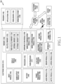
- FIG. 1 is a block diagram illustrating an electronic device 101 in a network environment 100 according to various embodiments.
- the electronic device 101 in the network environment 100 may communicate with an electronic device 102 via a first network 198 (e.g., a short-range wireless communication network), or at least one of an electronic device 104 or a server 108 via a second network 199 (e.g., a long-range wireless communication network).
- the electronic device 101 may communicate with the electronic device 104 via the server 108.
- the electronic device 101 may include a processor 120, memory 130, an input module 150, a sound output module 155, a display module 160, an audio module 170, a sensor module 176, an interface 177, a connecting terminal 178, a haptic module 179, a camera module 180, a power management module 188, a battery 189, a communication module 190, a subscriber identification module(SIM) 196, or an antenna module 197.
- at least one of the components e.g., the connecting terminal 178) may be omitted from the electronic device 101, or one or more other components may be added in the electronic device 101.
- some of the components e.g., the sensor module 176, the camera module 180, or the antenna module 197) may be implemented as a single component (e.g., the display module 160).
- the processor 120 may execute, for example, software (e.g., a program 140) to control at least one other component (e.g., a hardware or software component) of the electronic device 101 coupled with the processor 120, and may perform various data processing or computation. According to one embodiment, as at least part of the data processing or computation, the processor 120 may store a command or data received from another component (e.g., the sensor module 176 or the communication module 190) in volatile memory 132, process the command or the data stored in the volatile memory 132, and store resulting data in non-volatile memory 134.
- software e.g., a program 140
- the processor 120 may store a command or data received from another component (e.g., the sensor module 176 or the communication module 190) in volatile memory 132, process the command or the data stored in the volatile memory 132, and store resulting data in non-volatile memory 134.
- the processor 120 may include a main processor 121 (e.g., a central processing unit (CPU) or an application processor (AP)), or an auxiliary processor 123 (e.g., a graphics processing unit (GPU), a neural processing unit (NPU), an image signal processor (ISP), a sensor hub processor, or a communication processor (CP)) that is operable independently from, or in conjunction with, the main processor 121.
- a main processor 121 e.g., a central processing unit (CPU) or an application processor (AP)
- auxiliary processor 123 e.g., a graphics processing unit (GPU), a neural processing unit (NPU), an image signal processor (ISP), a sensor hub processor, or a communication processor (CP)
- the main processor 121 may be adapted to consume less power than the main processor 121, or to be specific to a specified function.
- the auxiliary processor 123 may be implemented as separate from, or as part of the main processor 121.
- the auxiliary processor 123 may control at least some of functions or states related to at least one component (e.g., the display module 160, the sensor module 176, or the communication module 190) among the components of the electronic device 101, instead of the main processor 121 while the main processor 121 is in an inactive (e.g., sleep) state, or together with the main processor 121 while the main processor 121 is in an active state (e.g., executing an application).
- the auxiliary processor 123 e.g., an image signal processor or a communication processor
- the auxiliary processor 123 may include a hardware structure specified for artificial intelligence model processing.
- An artificial intelligence model may be generated by machine learning. Such learning may be performed, e.g., by the electronic device 101 where the artificial intelligence is performed or via a separate server (e.g., the server 108). Learning algorithms may include, but are not limited to, e.g., supervised learning, unsupervised learning, semi-supervised learning, or reinforcement learning.
- the artificial intelligence model may include a plurality of artificial neural network layers.
- the artificial neural network may be a deep neural network (DNN), a convolutional neural network (CNN), a recurrent neural network (RNN), a restricted boltzmann machine (RBM), a deep belief network (DBN), a bidirectional recurrent deep neural network (BRDNN), deep Q-network or a combination of two or more thereof but is not limited thereto.
- the artificial intelligence model may, additionally or alternatively, include a software structure other than the hardware structure.
- the memory 130 may store various data used by at least one component (e.g., the processor 120 or the sensor module 176) of the electronic device 101.
- the various data may include, for example, software (e.g., the program 140) and input data or output data for a command related thererto.
- the memory 130 may include the volatile memory 132 or the non-volatile memory 134.
- the program 140 may be stored in the memory 130 as software, and may include, for example, an operating system (OS) 142, middleware 144, or an application 146.
- OS operating system
- middleware middleware
- application application
- the input module 150 may receive a command or data to be used by another component (e.g., the processor 120) of the electronic device 101, from the outside (e.g., a user) of the electronic device 101.
- the input module 150 may include, for example, a microphone, a mouse, a keyboard, a key (e.g., a button), or a digital pen (e.g., a stylus pen).
- the sound output module 155 may output sound signals to the outside of the electronic device 101.
- the sound output module 155 may include, for example, a speaker or a receiver.
- the speaker may be used for general purposes, such as playing multimedia or playing record.
- the receiver may be used for receiving incoming calls. According to an embodiment, the receiver may be implemented as separate from, or as part of the speaker.
- the audio module 170 may convert a sound into an electrical signal and vice versa. According to an embodiment, the audio module 170 may obtain the sound via the input module 150, or output the sound via the sound output module 155 or a headphone of an external electronic device (e.g., an electronic device 102) directly (e.g., wiredly) or wirelessly coupled with the electronic device 101.
- an external electronic device e.g., an electronic device 102
- directly e.g., wiredly
- wirelessly e.g., wirelessly
- the interface 177 may support one or more specified protocols to be used for the electronic device 101 to be coupled with the external electronic device (e.g., the electronic device 102) directly (e.g., wiredly) or wirelessly.
- the interface 177 may include, for example, a high definition multimedia interface (HDMI), a universal serial bus (USB) interface, a secure digital (SD) card interface, or an audio interface.
- HDMI high definition multimedia interface
- USB universal serial bus
- SD secure digital
- a connecting terminal 178 may include a connector via which the electronic device 101 may be physically connected with the external electronic device (e.g., the electronic device 102).
- the connecting terminal 178 may include, for example, a HDMI connector, a USB connector, a SD card connector, or an audio connector (e.g., a headphone connector).
- the haptic module 179 may convert an electrical signal into a mechanical stimulus (e.g., a vibration or a movement) or electrical stimulus which may be recognized by a user via his tactile sensation or kinesthetic sensation.
- the haptic module 179 may include, for example, a motor, a piezoelectric element, or an electric stimulator.
- the camera module 180 may capture a still image or moving images.
- the camera module 180 may include one or more lenses, image sensors, image signal processors, or flashes.
- the power management module 188 may manage power supplied to the electronic device 101.
- the power management module 188 may be implemented as at least part of, for example, a power management integrated circuit (PMIC).
- PMIC power management integrated circuit
- the communication module 190 may support establishing a direct (e.g., wired) communication channel or a wireless communication channel between the electronic device 101 and the external electronic device (e.g., the electronic device 102, the electronic device 104, or the server 108) and performing communication via the established communication channel.
- the communication module 190 may include one or more communication processors that are operable independently from the processor 120 (e.g., the application processor (AP)) and supports a direct (e.g., wired) communication or a wireless communication.
- AP application processor
- the communication module 190 may include a wireless communication module 192 (e.g., a cellular communication module, a short-range wireless communication module, or a global navigation satellite system (GNSS) communication module) or a wired communication module 194 (e.g., a local area network (LAN) communication module or a power line communication (PLC) module).
- a wireless communication module 192 e.g., a cellular communication module, a short-range wireless communication module, or a global navigation satellite system (GNSS) communication module
- GNSS global navigation satellite system
- wired communication module 194 e.g., a local area network (LAN) communication module or a power line communication (PLC) module.
- LAN local area network
- PLC power line communication
- a corresponding one of these communication modules may communicate with the external electronic device via the first network 198 (e.g., a short-range communication network, such as Bluetooth TM , wireless-fidelity (Wi-Fi) direct, or infrared data association (IrDA)) or the second network 199 (e.g., a long-range communication network, such as a legacy cellular network, a 5G network, a next-generation communication network, the Internet, or a computer network (e.g., LAN or wide area network (WAN)).
- first network 198 e.g., a short-range communication network, such as Bluetooth TM , wireless-fidelity (Wi-Fi) direct, or infrared data association (IrDA)
- the second network 199 e.g., a long-range communication network, such as a legacy cellular network, a 5G network, a next-generation communication network, the Internet, or a computer network (e.g., LAN or wide area network (WAN)).
- the wireless communication module 192 may identify and authenticate the electronic device 101 in a communication network, such as the first network 198 or the second network 199, using subscriber information (e.g., international mobile subscriber identity (IMSI)) stored in the subscriber identification module 196.
- subscriber information e.g., international mobile subscriber identity (IMSI)
- the wireless communication module 192 may support various technologies for securing performance on a high-frequency band, such as, e.g., beamforming, massive multiple-input and multiple-output (massive MIMO), full dimensional MIMO (FD-MIMO), array antenna, analog beam-forming, or large scale antenna.
- the wireless communication module 192 may support various requirements specified in the electronic device 101, an external electronic device (e.g., the electronic device 104), or a network system (e.g., the second network 199).
- the antenna module 197 may transmit or receive a signal or power to or from the outside (e.g., the external electronic device) of the electronic device 101.
- the antenna module 197 may include an antenna including a radiating element composed of a conductive material or a conductive pattern formed in or on a substrate (e.g., a printed circuit board (PCB)).
- the antenna module 197 may include a plurality of antennas (e.g., array antennas). In such a case, at least one antenna appropriate for a communication scheme used in the communication network, such as the first network 198 or the second network 199, may be selected, for example, by the communication module 190 (e.g., the wireless communication module 192) from the plurality of antennas.
- At least some of the above-described components may be coupled mutually and communicate signals (e.g., commands or data) therebetween via an inter-peripheral communication scheme (e.g., a bus, general purpose input and output (GPIO), serial peripheral interface (SPI), or mobile industry processor interface (MIPI)).
- an inter-peripheral communication scheme e.g., a bus, general purpose input and output (GPIO), serial peripheral interface (SPI), or mobile industry processor interface (MIPI)
- commands or data may be transmitted or received between the electronic device 101 and the external electronic device 104 via the server 108 coupled with the second network 199.
- Each of the electronic devices 102 or 104 may be a device of a same type as, or a different type, from the electronic device 101.
- all or some of operations to be executed at the electronic device 101 may be executed at one or more of the external electronic devices 102, 104, or 108. For example, if the electronic device 101 should perform a function or a service automatically, or in response to a request from a user or another device, the electronic device 101, instead of, or in addition to, executing the function or the service, may request the one or more external electronic devices to perform at least part of the function or the service.
- the external electronic device 104 or the server 108 may be included in the second network 199.
- the electronic device 101 may be applied to intelligent services (e.g., smart home, smart city, smart car, or healthcare) based on 5G communication technology or IoT-related technology.
- the electronic device may be one of various types of electronic devices.
- the electronic devices may include, for example, a portable communication device (e.g., a smartphone), a computer device, a portable multimedia device, a portable medical device, a camera, a wearable device, or a home appliance. According to an embodiment of the disclosure, the electronic devices are not limited to those described above.
- each of such phrases as “A or B,” “at least one of A and B,” “at least one of A or B,” “A, B, or C,” “at least one of A, B, and C,” and “at least one of A, B, or C,” may include any one of, or all possible combinations of the items enumerated together in a corresponding one of the phrases.
- such terms as “1st” and “2nd,” or “first” and “second” may be used to simply distinguish a corresponding component from another, and does not limit the components in other aspect (e.g., importance or order).
- an element e.g., a first element
- the element may be coupled with the other element directly (e.g., wiredly), wirelessly, or via a third element.
- Various embodiments as set forth herein may be implemented as software (e.g., the program 140) including one or more instructions that are stored in a storage medium (e.g., internal memory 136 or external memory 138) that is readable by a machine (e.g., the electronic device 101).
- a processor e.g., the processor 120
- the machine e.g., the electronic device 101
- the one or more instructions may include a code generated by a complier or a code executable by an interpreter.
- the machine-readable storage medium may be provided in the form of a non-transitory storage medium.
- non-transitory simply means that the storage medium is a tangible device, and does not include a signal (e.g., an electromagnetic wave), but this term does not differentiate between where data is semi-permanently stored in the storage medium and where the data is temporarily stored in the storage medium.
- each component e.g., a module or a program of the above-described components may include a single entity or multiple entities, and some of the multiple entities may be separately disposed in different components. According to various embodiments, one or more of the above-described components may be omitted, or one or more other components may be added. Alternatively or additionally, a plurality of components (e.g., modules or programs) may be integrated into a single component. In such a case, according to various embodiments, the integrated component may still perform one or more functions of each of the plurality of components in the same or similar manner as they are performed by a corresponding one of the plurality of components before the integration.
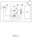
- FIG. 2 is a block diagram illustrating a construction of an electronic device 101 according to an embodiment.
- An electronic device 101 of an embodiment may include a memory 130 and a processor 200 (e.g., processor 120 of FIG. 1 and main processor 121 of FIG. 1 ).
- the processor 200 may include, for example, an application processor, which is a system semiconductor that performs the driving of various application programs, graphic processing, etc. in the electronic device 101.
- the processor 200 may include a neural network processing unit 210 and a central processing unit 220.
- the neural network processing unit 210 may include a device configured to efficiently process parallel computations and process a neural network model.
- the neural network processing unit 210 may be configured to perform a plurality of simple computations in parallel compared to the central processing unit 220.
- the central processing unit 220 may be configured to perform complex computations in series compared to the neural network processing unit 210.
- the neural network processing unit 210 and the central processing unit 220 of an embodiment may be integrated into the processor 200.
- the processor 200 of an embodiment may be configured to communicate the neural network processing unit 210 with the central processing unit 220.
- the processor 200 may be configured wherein the neural network processing unit 210 transmits or receives data to or from the central processing unit 220 without going through the memory 130.
- the neural network processing unit 210 may be connected to an interconnect 230.
- the interconnect 230 may be configured to connect the neural network processing unit 210 to an arbiter 221 of the central processing unit 220.
- the interconnect 230 may be connected to the neural network processing unit 210 and the central processing unit 220 through a physical interface (e.g., bus).
- the central processing unit 220 may include the arbiter 221 and a cache memory 223.
- the arbiter 221 may be configured to selectively connect the cache memory 223 to either a processing circuit for allowing the central processing unit 220 to process data or the interconnect 230.
- the arbiter 221 may include a circuit configured to perform a function presented in the disclosure, or a functional block implemented by the central processing unit 220.
- FIG. 3 is a block diagram illustrating a construction of a processor 200 including a plurality of core processors 320 according to an embodiment.
- a processor 200 of an embodiment may include a neural network processing unit 210, a central processing unit 220, an interconnect 230, a dynamic shared unit (DSU) 330, a cache coherent interconnect (CCI) 340, a system cache / bus 350, and a memory controller 360.
- FIG. 3 is for explaining an example of a construction of the processor 200 of an embodiment, and some components may be replaced with other components or be omitted.
- the names (e.g., dynamic shared unit, cache coherent interconnect) used in FIG. 3 are for explaining the components separately, and the names themselves do not limit the characteristics of the components.
- the central processing unit 220 of the electronic device 101 may include a plurality of core processors 320.
- the plurality of core processors 320 at least one core processor 321 may be configured to perform neural network computation for performing a neural network model in conjunction with the neural network processing unit 210.
- the at least one core processor 321 may include an arbiter 221, a cache memory 223, and a processing circuit 323.
- the cache memory 223 may include a memory temporarily storing data for fast data access.
- the cache memory 223 may include an L1 cache memory and an L2 cache memory.
- the processing circuit 323 may be configured to perform computation, based on input data.
- the arbiter 221 may connect the cache memory 223 to the processing circuit 323 or the interconnect 230.
- the neural network processing unit 210 may include an interrupt controller 311, a computing circuit 313, or static random access memory 315.
- the interrupt controller 311 may control an interrupt occurring in a computation procedure of the neural network processing unit 210.
- the interrupt controller 311 may be connected to the at least one core processor 321 of the central processing unit 220 and transfer an interrupt signal to the at least one core processor 321.
- the interrupt controller 311 may be physically directly connected to the central processing unit 220.
- the computing circuit 313 may perform computation of the neural network processing unit 210.
- the static random access memory 315 may store data that is used for computation performed by the neural network processing unit 210.
- the static random access memory 315 may store information that is input to a computation layer included in a neural network model.
- the neural network processing unit 210 may include a direct memory access (DMA) 317.
- the direct memory access 317 may be configured to transmit or receive data to or from the arbiter 221 via the interconnect 230.
- Data transferred between the neural network processing unit 210 and the central processing unit 220 may include feature information (e.g., feature map) that is input to or output from the neural network model.
- the direct memory access 317 may perform conversion between a first data format (e.g., INT8) used in the neural network processing unit 210 and a second data format (e.g., FP32) used in the central processing unit 220.
- the dynamic shared unit 330 may be connected to the central processing unit 220.
- the dynamic shared unit 330 may include a cache coherency control circuit that maintains cache coherency between the plurality of core processors 320.
- the dynamic shared unit 330 may further include an L3 cache memory presented to the central processing unit 220.
- the dynamic shared unit 330 may allocate a core processor for executing a process among the plurality of core processors 320.
- the dynamic shared unit 330 may allocate another process to another core processor except for the at least one core processor 321. According to an embodiment, even when the at least one core processor 321 is not exclusively used by the process performed in conjunction with the neural network processing unit 210, the at least one core processor 321 may be allocated a process at a low priority.
- the cache coherency interconnect 340 may be connected to a plurality subsystems.
- the cache coherency interconnect 340 may be connected to the interconnect 230 and the dynamic shared unit 330.
- the cache coherency interconnect 340 may include a bus that maintains cache coherency between the plurality of subsystems connected.
- the cache coherency interconnect 340 may be connected to the memory controller 360 via the system cache / bus 350.
- the memory controller 360 may access dynamic random access memory 370 (e.g., memory 130 of FIG. 2 ) and store data in or retrieve data from the dynamic random access memory 370.
- the arbiter 221 connects the cache memory 223 to the interconnect 230, and the direct memory access 317 transmits data to be stored in the shared memory area of the DRAM 370, the data may remain in the cache memory 223 (e.g., L1 cache) while going through the cache memory 223 in a procedure of transferring the data to the DRAM 370.
- the arbiter 221 connects the cache memory 223 to the processing circuit 323, and the processing circuit 323 loads data stored in the shared memory area of the DRAM 370, data stored in the cache memory 223 may be loaded. Accordingly, the data may be transferred from the neural network processing unit 210 to the central processing unit 220 without performing an operation of accessing the DRAM 370.
- the central processing unit 220 may write data to the DRAM 370 via the DSU 330, the CCI 340, the system cache / bus 350, and the memory controller 360.
- the neural network processing unit 210 may need to receive data from the central processing unit 220 by reading the data from the DRAM 370 via the CCI 340, the system cache / bus 350, and the memory controller 360.
- a delay may occur by sending and receiving data through the DRAM 370.
- a delay occurring in a procedure of switching a subject that computes a computation layer included in a neural network model may be reduced.
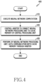
- FIG. 4 is a flowchart 400 illustrating a process in which an electronic device (e.g., electronic device 101 of FIGS. 1 and 2 ) operates according to an embodiment.
- an electronic device e.g., electronic device 101 of FIGS. 1 and 2 .
- an electronic device may execute neural network computation, based on a neural network model.
- a central processing unit e.g., central processing unit 220 of FIGS. 2 and 3
- the electronic device e.g., electronic device 101 of FIGS. 1 and 2
- the electronic device may control an arbiter (e.g., arbiter 221 of FIGS. 2 and 3 ) to connect the neural network processing unit (e.g., neural network processing unit 210 of FIGS. 2 and 3 ) to a cache memory (e.g., cache memory 223 of FIGS. 2 and 3 ) of the central processing unit (e.g., central processing unit 220 of FIGS. 2 and 3 ).
- an arbiter e.g., arbiter 221 of FIGS. 2 and 3
- the neural network processing unit e.g., neural network processing unit 210 of FIGS. 2 and 3
- a cache memory e.g., cache memory 223 of FIGS. 2 and 3
- the central processing unit e.g., central processing unit 220 of FIGS. 2 and 3
- the electronic device may allow the neural network processing unit (e.g., neural network processing unit 210 of FIGS. 2 and 3 ) to perform communication with the cache memory (e.g., cache memory 223 of FIGS. 2 and 3 ) of the central processing unit through the arbiter (e.g., arbiter 221 of FIGS. 2 and 3 ).
- the neural network processing unit e.g., neural network processing unit 210 of FIGS. 2 and 3
- the neural network processing unit e.g., neural network processing unit 210 of FIGS.
- the central processing unit e.g., central processing unit 220 of FIGS. 2 and 3
- the central processing unit e.g., central processing unit 220 of FIGS. 2 and 3
- the neural network processing unit e.g., neural network processing unit 210 of FIGS. 2 and 3
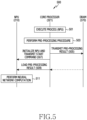
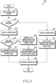
- FIG. 5 is a flowchart 500 illustrating a process for performing an operation including pre-processing for performing neural network computation by an electronic device (e.g., electronic device 101 of FIGS. 1 and 2 ) according to an embodiment.
- an electronic device e.g., electronic device 101 of FIGS. 1 and 2
- At least one core processor 321 may execute a process (NPU) for performing neural network computation in conjunction with a neural network processing unit 210.
- the at least one core processor 321 may be exclusively used by the process for performing in conjunction with the neural network processing unit 210.
- An electronic device e.g., electronic device 101 of FIGS. 1 and 2 ) may determine whether the process for performing in conjunction with the neural network processing unit 210 will exclusively use the at least one core processor 321, based on a parameter defining whether to exclusively use the at least one core processor 321.
- the parameter may be configured as a value included in a file for executing a neural network model.
- the process for performing in conjunction with the neural network processing unit 210 may exclusively use the at least one core processor 321.
- the process for performing in conjunction with the neural network processing unit 210 may exclusively use the at least one core processor 321.
- the at least one core processor 321 may further perform another process.
- the at least one core processor 321 may further perform another process.
- the at least one core processor 321 may perform a pre-processing operation on input data to be input to the neural network model. For example, when sentences composed of natural language are to be processed using a neural network model for performing natural language processing, since the sentences may not be directly input to the neural network model, the core processor 321 may perform at least one of an operation of tokenizing the sentences by the unit of sentence, an operation of tokenizing the sentences by the unit of word, or an operation of tokenizing the sentences by the unit of character.
- the pre-processing operation may be configured in various ways depending on the neural network model.
- the at least one core processor 321 may initialize the neural network processing unit 210 and transfer a start command for neural network computation to the neural network processing unit 210. After transferring the start command to the neural network processing unit 210, the at least one core processor 321 may wait until an interrupt signal is received from the neural network processing unit 210. When the at least one core processor 321 is exclusively used by the process for performing in conjunction with the neural network processing unit 210, the at least one core processor 321 may not perform context switching.
- the neural network processing unit 210 may perform neural network computation, based on the loaded pre-processing result. For example, the neural network processing unit 210 may input the pre-processing result to a first computation layer of the neural network model and perform computation on the first computation layer.
- a neural network processing unit 210 may perform computation on a second computation layer.
- the second computation layer is a layer before a first computation layer being an N+1th computation layer among a plurality of computation layers included in a neural network model, and is an Nth computation layer in the neural network model.
- the neural network processing unit 210 may input the pre-processing result loaded in operation 509 of FIG. 5 to the second computation layer, and perform computation on the second computation layer.
- the neural network processing unit 210 may input a value output from an N-1th computation layer, to the second computation layer, and perform computation on the second computation layer.
- the neural network processing unit 210 may obtain first feature information (e.g., feature map) that is output by performing the computation on the second computation layer.
- the neural network processing unit 210 may transmit, to the DRAM 370, the first feature information that is obtained by performing the computation on the second computation layer.
- a direct memory access (e.g., direct memory access 317 of FIG. 3 ) may transmit the first feature information to the DRAM 370 via a path (e.g., DSU 330, CCI 340, system cache / bus 350, and memory controller 360 of FIG. 3 ) going from an interconnect (e.g., interconnect 230 of FIGS. 2 and 3 ), an arbiter (e.g., arbiter 221 of FIGS. 2 and 3 ), a cache memory
- an interconnect e.g., interconnect 230 of FIGS. 2 and 3
- an arbiter e.g., arbiter 221 of FIGS. 2 and 3
- the first feature information may be written to the cache memory (e.g., cache memory 223 of FIGS. 2 and 3 ).
- the core processor 321 may read the first feature information.
- the core processor 321 since the first feature information is written to the cache memory (e.g., cache memory 223 of FIGS. 2 and 3 ) of the core processor 321, the core processor 321 may obtain the first feature information from the cache memory (e.g., cache memory 223 of FIGS. 2 and 3 ). Therefore, the core processor 321 may obtain the first feature information without overhead occurring for accessing the DRAM 370.
- the core processor 321 may input the obtained first feature information to the first computation layer and perform the computation on the first computation layer.
- FIG. 7 is a flowchart 700 illustrating a process for performing computation on a next computation layer by a neural network processing unit, based on the result of computation on a computation layer performed by a core processor (e.g., at least one core processor 321 of FIG. 3 ) of a central processing unit (e.g., central processing unit 220 of FIGS. 2 and 3 ) of an electronic device (e.g., electronic device 101 of FIGS. 1 and 2 ) according to an embodiment.
- a core processor e.g., at least one core processor 321 of FIG. 3
- a central processing unit e.g., central processing unit 220 of FIGS. 2 and 3
- an electronic device e.g., electronic device 101 of FIGS. 1 and 2
- the core processor 321 may perform computation on a first computation layer being an N+1th computation layer in a neural network model. For example, the core processor 321 may obtain second feature information that is output by inputting first feature information to the first computation layer.
- arbiter e.g., arbiter 221 of FIGS. 2 and 3
- cache memory e.g., cache memory 223 of FIGS. 2 and 3
- central processing unit e.g., central processing unit 220 of FIGS. 2 and 3
- the arbiter e.g., arbiter 221 of FIGS. 2 and 3
- may transfer the second feature information output from the processing circuit e.g., processing circuit 323 of FIG. 3 ), to the cache memory 223.
- the core processor 321 may transmit an interrupt signal for allowing to perform computation on a third computation layer that is an N+2th computation layer in the neural network model, to the neural network processing unit 210.
- the neural network processing unit 210 may perform the computation on the third computation layer, based on the second feature information. For example, the neural network processing unit 210 may input the second feature information to the third computation layer and perform the computation on the third computation layer.
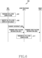
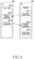
- FIG. 8 is a diagram illustrating an operation in which a neural network processing unit 210 and a central processing unit 220 communicate without going through a memory and perform neural network computation according to an embodiment.
- the neural network processing unit may perform computation on an Nth computation layer in the neural network model. After performing the computation operation on the Nth computation layer, the neural network processing unit may identify that computation on an N+1th computation layer should be performed by the central processing unit. The neural network processing unit may perform an operation of storing feature information for performing the computation on the N+1th computation layer in a shared memory area of a memory. The feature information for performing the computation on the N+1th computation layer may include information that is obtained as the result of the computation on the Nth computation layer. In this operation, a memory access overhead may occur in order for the neural network processing unit to access a memory.
- the central processing unit may perform an operation of reading feature information for performing the computation on the N+1th computation layer from a memory, based on a process.
- a memory access overhead may occur again in order for the central processing unit to access the memory.
- the central processing unit may perform a computation operation on the N+1th computation layer, based on the read feature information.
- the central processing unit may perform an operation of storing feature information for performing computation on an N+2th computation layer in a shared memory area of the memory.
- the feature information for performing the computation on the N+2th computation layer may include information obtained as the result of performing the computation on the N+1th computation layer.
- a memory access overhead may occur in order for the central processing unit to access the memory.
- the central processing unit 220 of an embodiment may be exclusively used by a process 801-3 for performing computation that is based on a neural network model. For example, while computations are performed on computation layers for which a corresponding parameter (parameter indicating whether a core processor is exclusively used) is set to ON, at least one processor (e.g., at least one core processor 321 of FIG. 3 ) of the central processing unit 220 may execute only the process 801-3. Accordingly, while the process 801-3 is executed, a delay due to context switching may be prevented.
- a corresponding parameter parameter indicating whether a core processor is exclusively used
- the neural network processing unit 210 of an embodiment may perform a computation operation 811-2 on an Nth computation layer included in a neural network model.
- the neural network processing unit 210 may transfer feature information for performing the computation on the N+1th computation layer, to a cache memory (e.g., L1 cache memory) of the central processing unit 220.
- the central processing unit 220 may perform an operation 819-2 for reading feature information for performing the computation on the N+1th computation layer, stored in the cache memory. Since the central processing unit 220 may read the feature information from the cache memory, the central processing unit 220 may obtain the feature information fast without a memory access overhead.
- the central processing unit 220 may perform the computation operation 821-2 on the N+1th computation layer, based on the feature information.
- the result of performing the computation on the N+1th computation layer may be written to the cache memory of the central processing unit 220.
- the neural network processing unit 210 may perform an operation 825-2 of reading feature information written to the cache memory of the central processing unit 220.
- the feature information may include information obtained as the result of performing the computation on the N+1th computation layer. Since the neural network processing unit 210 of an embodiment may read the feature information written to the cache memory, a memory access overhead for accessing DRAM (e.g., DRAM 370 of FIG. 3 ) may be prevented.
- the neural network processing unit 210 may perform a computation operation 827-2 on an N+2th computation layer, based on the feature information obtained from the cache memory.
- An electronic device of an embodiment may include a memory, and a processor operatively connected to the memory.
- the processor may include a central processing unit including a cache memory, a neural network processing unit, and an interconnect connected to the neural network processing unit.
- the central processing unit may include an arbiter for connecting the cache memory to any one of a processing circuit of the central processing unit or the interconnect.
- the neural network processing unit may be configured to exchange data with the cache memory through the arbiter
- the direct memory access may be configured to convert a first data format used in the neural network processing unit into a second data format used in the central processing unit, and transmit the feature data from the neural network processing unit to the central processing unit.
- the first feature information may include information that is output from a second computation layer included in the neural network computation by performing computation on the second computation layer by the neural network processing unit.
- the central processing unit of the electronic device of an embodiment may be configured to, in a procedure of compiling the file of the neural network model, identify at least one computation layer on which computation should be performed by the central processing unit, among a plurality of computation layers included in the neural network computation.
- the central processing unit may be configured to, in the compiling procedure, specify values of parameters for each of the plurality of computation layers, based on the identified at least one computation layer.
- An operating method of an electronic device of an embodiment may include executing neural network computation by a neural network processing unit of the electronic device.
- the method may include controlling an arbiter included in a central processing unit of the electronic device to connect a cache memory of the central processing unit to an interconnect connected to the neural network processing unit.
- the method may include receiving data for performing the executed neural network computation by the neural network processing unit, from the cache memory through the arbiter, or transmitting the data to the cache memory through the arbiter.
- programs may be stored in random access memory, non-volatile memory including flash memory, read only memory (ROM), electrically erasable programmable ROM (EEPROM), magnetic disc storage device, compact disc-ROM (CD-ROM), digital versatile discs (DVDs) or other types of optical storage devices, and magnetic cassette.
- ROM read only memory
- EEPROM electrically erasable programmable ROM
- magnetic disc storage device compact disc-ROM (CD-ROM), digital versatile discs (DVDs) or other types of optical storage devices
- CD-ROM compact disc-ROM
- DVDs digital versatile discs
- the programs may be stored in a memory composed of a combination of some or all of them.
- each composed memory may be included in multiples as well.
- the terms “unit”, “module”, etc. may include a hardware component such as a processor or a circuit, and/or a software component executed by the hardware component such as the processor.
- Unit and module may be also implemented by a program that may be stored in an addressable storage medium and executed by the processor.
- unit and “module” may be implemented by components, such as software components, object-oriented software components, class components, and task components, processes, functions, properties, procedures, subroutines, segments of a program code, drivers, firmware, microcode, circuits, data, databases, data structures, tables, arrays, and variables.
- “including at least one of a, b, or c” may mean “including only a”, “including only b”, “including only c", “including a and b”, “including b and c”, “including a and c", or "including all of a, b, and c”.
Landscapes
- Engineering & Computer Science (AREA)
- Theoretical Computer Science (AREA)
- Software Systems (AREA)
- Physics & Mathematics (AREA)
- General Engineering & Computer Science (AREA)
- General Physics & Mathematics (AREA)
- Biomedical Technology (AREA)
- Biophysics (AREA)
- Life Sciences & Earth Sciences (AREA)
- Health & Medical Sciences (AREA)
- Molecular Biology (AREA)
- Computational Linguistics (AREA)
- Data Mining & Analysis (AREA)
- Evolutionary Computation (AREA)
- General Health & Medical Sciences (AREA)
- Artificial Intelligence (AREA)
- Computing Systems (AREA)
- Mathematical Physics (AREA)
- Computer Hardware Design (AREA)
- Neurology (AREA)
- Advance Control (AREA)
Applications Claiming Priority (3)
| Application Number | Priority Date | Filing Date | Title |
|---|---|---|---|
| KR20220117069 | 2022-09-16 | ||
| KR1020220131586A KR20240038531A (ko) | 2022-09-16 | 2022-10-13 | 신경 처리부를 포함하는 전자 장치 및 그 동작 방법 |
| PCT/KR2023/013962 WO2024058615A1 (ko) | 2022-09-16 | 2023-09-15 | 신경 처리부를 포함하는 전자 장치 및 그 동작 방법 |
Publications (2)
| Publication Number | Publication Date |
|---|---|
| EP4575772A1 true EP4575772A1 (de) | 2025-06-25 |
| EP4575772A4 EP4575772A4 (de) | 2025-12-24 |
Family
ID=90275442
Family Applications (1)
| Application Number | Title | Priority Date | Filing Date |
|---|---|---|---|
| EP23865910.6A Pending EP4575772A4 (de) | 2022-09-16 | 2023-09-15 | Elektronische vorrichtung mit neuronaler verarbeitungseinheit und betriebsverfahren dafür |
Country Status (4)
| Country | Link |
|---|---|
| US (1) | US20250225096A1 (de) |
| EP (1) | EP4575772A4 (de) |
| CN (1) | CN119895386A (de) |
| WO (1) | WO2024058615A1 (de) |
Family Cites Families (6)
| Publication number | Priority date | Publication date | Assignee | Title |
|---|---|---|---|---|
| US20060112226A1 (en) * | 2004-11-19 | 2006-05-25 | Hady Frank T | Heterogeneous processors sharing a common cache |
| JP2015219606A (ja) * | 2014-05-14 | 2015-12-07 | ローム株式会社 | 演算処理システム、信号処理回路、電子機器 |
| US10664751B2 (en) * | 2016-12-01 | 2020-05-26 | Via Alliance Semiconductor Co., Ltd. | Processor with memory array operable as either cache memory or neural network unit memory |
| US11861484B2 (en) * | 2018-09-28 | 2024-01-02 | Qualcomm Incorporated | Neural processing unit (NPU) direct memory access (NDMA) hardware pre-processing and post-processing |
| KR102518057B1 (ko) * | 2019-12-12 | 2023-04-06 | 한국전자통신연구원 | 인공지능 프로세서를 위한 캐시 |
| US20210390004A1 (en) * | 2020-06-16 | 2021-12-16 | Nvidia Corporation | Accelerated fifth generation (5g) new radio operations |
-
2023
- 2023-09-15 WO PCT/KR2023/013962 patent/WO2024058615A1/ko not_active Ceased
- 2023-09-15 CN CN202380066710.1A patent/CN119895386A/zh active Pending
- 2023-09-15 EP EP23865910.6A patent/EP4575772A4/de active Pending
-
2025
- 2025-03-14 US US19/079,977 patent/US20250225096A1/en active Pending
Also Published As
| Publication number | Publication date |
|---|---|
| US20250225096A1 (en) | 2025-07-10 |
| WO2024058615A1 (ko) | 2024-03-21 |
| CN119895386A (zh) | 2025-04-25 |
| EP4575772A4 (de) | 2025-12-24 |
Similar Documents
| Publication | Publication Date | Title |
|---|---|---|
| US20220309352A1 (en) | Method for training artificial neural network and electronic device for supporting the same | |
| US20230214262A1 (en) | Electronic device for managing memory, operation method of electronic device, and non-transitory storage medium | |
| US20220245515A1 (en) | Electronic device for performing computation based on artificial intelligence model and operation method thereof | |
| EP4575772A1 (de) | Elektronische vorrichtung mit neuronaler verarbeitungseinheit und betriebsverfahren dafür | |
| US12229427B2 (en) | Electronic device and operation method of electronic device for managing storage space | |
| US12130728B2 (en) | Electronic device and method controlling the same | |
| US12314831B2 (en) | Electronic device for rearranging kernels of neural network and operating method thereof | |
| US12287983B2 (en) | Data swapping method and electronic device supporting same | |
| US12229539B2 (en) | Application optimization method and apparatus supporting the same | |
| EP4296904B1 (de) | Elektronische vorrichtung zur verarbeitung eines modells eines neuronalen netzwerks und betriebsverfahren dafür | |
| EP4261688A1 (de) | Elektronische vorrichtung zur durchführung eines tests zur fehlererkennung einer elektronischen vorrichtung und verfahren zur durchführung eines tests zur fehlererkennung einer elektronischen vorrichtung | |
| US20220130396A1 (en) | Electronic device for managing user model and operating method thereof | |
| US20250045564A1 (en) | Electronic device and method for driving models on basis of information commonly used by models | |
| KR20230023281A (ko) | 인공 신경망 모델을 포함하는 전자 장치 및 전자 장치의 동작 방법 | |
| US20240202590A1 (en) | Electronic device and operation method of electronic device for performing calculation using artificial intelligence model | |
| KR20240038531A (ko) | 신경 처리부를 포함하는 전자 장치 및 그 동작 방법 | |
| EP4258114A1 (de) | Dienstbetriebsverfahren und elektronische vorrichtung zur unterstützung davon | |
| US20240289654A1 (en) | Electronic device and operation method of electronic device for performing calculation using artificial intelligence model | |
| EP4693003A1 (de) | Anwendungsausführungsverfahren und elektronische vorrichtung zur unterstützung davon | |
| US12056498B2 (en) | Electronic device for booting operating system using plurality of cores and operation method thereof | |
| US12340857B2 (en) | Electronic device for adjusting driving voltage of volatile memory and method for operating the same | |
| US20250238225A1 (en) | Apparatus and method for providing customizing software | |
| EP4191393B1 (de) | Elektronische vorrichtung und verfahren zur verwaltung des speichers einer elektronischen vorrichtung | |
| US20250371423A1 (en) | Electronic device providing results output through shared artificial intelligence model to multiple applications and method for controlling the same | |
| KR20240131211A (ko) | 인공지능 모델을 이용하여 연산을 수행하는 전자 장치 및 전자 장치의 동작 방법 |
Legal Events
| Date | Code | Title | Description |
|---|---|---|---|
| STAA | Information on the status of an ep patent application or granted ep patent |
Free format text: STATUS: THE INTERNATIONAL PUBLICATION HAS BEEN MADE |
|
| PUAI | Public reference made under article 153(3) epc to a published international application that has entered the european phase |
Free format text: ORIGINAL CODE: 0009012 |
|
| STAA | Information on the status of an ep patent application or granted ep patent |
Free format text: STATUS: REQUEST FOR EXAMINATION WAS MADE |
|
| 17P | Request for examination filed |
Effective date: 20250318 |
|
| AK | Designated contracting states |
Kind code of ref document: A1 Designated state(s): AL AT BE BG CH CY CZ DE DK EE ES FI FR GB GR HR HU IE IS IT LI LT LU LV MC ME MK MT NL NO PL PT RO RS SE SI SK SM TR |
|
| A4 | Supplementary search report drawn up and despatched |
Effective date: 20251121 |
|
| DAV | Request for validation of the european patent (deleted) | ||
| DAX | Request for extension of the european patent (deleted) | ||
| RIC1 | Information provided on ipc code assigned before grant |
Ipc: G06F 9/38 20180101AFI20251117BHEP Ipc: G06F 9/48 20060101ALI20251117BHEP Ipc: G06F 13/16 20060101ALI20251117BHEP Ipc: G06N 3/063 20230101ALI20251117BHEP Ipc: G06F 8/41 20180101ALI20251117BHEP Ipc: G06F 9/30 20180101ALI20251117BHEP Ipc: G06F 9/445 20180101ALI20251117BHEP Ipc: G06F 9/50 20060101ALI20251117BHEP Ipc: G06F 9/54 20060101ALI20251117BHEP Ipc: G06N 3/04 20230101ALI20251117BHEP Ipc: G06N 3/045 20230101ALI20251117BHEP Ipc: G06N 3/08 20230101ALI20251117BHEP |