EP4575475A1 - Systèmes et procédés d'analyse d'un échantillon à l'aide de faisceaux de particules chargées et de capteurs à pixels actifs commandés - Google Patents
Systèmes et procédés d'analyse d'un échantillon à l'aide de faisceaux de particules chargées et de capteurs à pixels actifs commandés Download PDFInfo
- Publication number
- EP4575475A1 EP4575475A1 EP24218633.6A EP24218633A EP4575475A1 EP 4575475 A1 EP4575475 A1 EP 4575475A1 EP 24218633 A EP24218633 A EP 24218633A EP 4575475 A1 EP4575475 A1 EP 4575475A1
- Authority
- EP
- European Patent Office
- Prior art keywords
- charged particle
- unidimensional
- data
- sample
- readout circuit
- Prior art date
- Legal status (The legal status is an assumption and is not a legal conclusion. Google has not performed a legal analysis and makes no representation as to the accuracy of the status listed.)
- Pending
Links
Images


Classifications
-
- G—PHYSICS
- G01—MEASURING; TESTING
- G01N—INVESTIGATING OR ANALYSING MATERIALS BY DETERMINING THEIR CHEMICAL OR PHYSICAL PROPERTIES
- G01N23/00—Investigating or analysing materials by the use of wave or particle radiation, e.g. X-rays or neutrons, not covered by groups G01N3/00 – G01N17/00, G01N21/00 or G01N22/00
- G01N23/22—Investigating or analysing materials by the use of wave or particle radiation, e.g. X-rays or neutrons, not covered by groups G01N3/00 – G01N17/00, G01N21/00 or G01N22/00 by measuring secondary emission from the material
- G01N23/225—Investigating or analysing materials by the use of wave or particle radiation, e.g. X-rays or neutrons, not covered by groups G01N3/00 – G01N17/00, G01N21/00 or G01N22/00 by measuring secondary emission from the material using electron or ion
- G01N23/2251—Investigating or analysing materials by the use of wave or particle radiation, e.g. X-rays or neutrons, not covered by groups G01N3/00 – G01N17/00, G01N21/00 or G01N22/00 by measuring secondary emission from the material using electron or ion using incident electron beams, e.g. scanning electron microscopy [SEM]
-
- G—PHYSICS
- G01—MEASURING; TESTING
- G01N—INVESTIGATING OR ANALYSING MATERIALS BY DETERMINING THEIR CHEMICAL OR PHYSICAL PROPERTIES
- G01N23/00—Investigating or analysing materials by the use of wave or particle radiation, e.g. X-rays or neutrons, not covered by groups G01N3/00 – G01N17/00, G01N21/00 or G01N22/00
- G01N23/20—Investigating or analysing materials by the use of wave or particle radiation, e.g. X-rays or neutrons, not covered by groups G01N3/00 – G01N17/00, G01N21/00 or G01N22/00 by using diffraction of the radiation by the materials, e.g. for investigating crystal structure; by using scattering of the radiation by the materials, e.g. for investigating non-crystalline materials; by using reflection of the radiation by the materials
- G01N23/203—Measuring back scattering
-
- H—ELECTRICITY
- H01—ELECTRIC ELEMENTS
- H01J—ELECTRIC DISCHARGE TUBES OR DISCHARGE LAMPS
- H01J37/00—Discharge tubes with provision for introducing objects or material to be exposed to the discharge, e.g. for the purpose of examination or processing thereof
- H01J37/02—Details
- H01J37/244—Detectors; Associated components or circuits therefor
-
- H—ELECTRICITY
- H01—ELECTRIC ELEMENTS
- H01J—ELECTRIC DISCHARGE TUBES OR DISCHARGE LAMPS
- H01J37/00—Discharge tubes with provision for introducing objects or material to be exposed to the discharge, e.g. for the purpose of examination or processing thereof
- H01J37/26—Electron or ion microscopes; Electron or ion diffraction tubes
- H01J37/28—Electron or ion microscopes; Electron or ion diffraction tubes with scanning beams
-
- G—PHYSICS
- G01—MEASURING; TESTING
- G01N—INVESTIGATING OR ANALYSING MATERIALS BY DETERMINING THEIR CHEMICAL OR PHYSICAL PROPERTIES
- G01N2223/00—Investigating materials by wave or particle radiation
- G01N2223/40—Imaging
- G01N2223/413—Imaging sensor array [CCD]
-
- G—PHYSICS
- G01—MEASURING; TESTING
- G01N—INVESTIGATING OR ANALYSING MATERIALS BY DETERMINING THEIR CHEMICAL OR PHYSICAL PROPERTIES
- G01N2223/00—Investigating materials by wave or particle radiation
- G01N2223/40—Imaging
- G01N2223/418—Imaging electron microscope
-
- H—ELECTRICITY
- H01—ELECTRIC ELEMENTS
- H01J—ELECTRIC DISCHARGE TUBES OR DISCHARGE LAMPS
- H01J2237/00—Discharge tubes exposing object to beam, e.g. for analysis treatment, etching, imaging
- H01J2237/244—Detection characterized by the detecting means
- H01J2237/2441—Semiconductor detectors, e.g. diodes
-
- H—ELECTRICITY
- H01—ELECTRIC ELEMENTS
- H01J—ELECTRIC DISCHARGE TUBES OR DISCHARGE LAMPS
- H01J2237/00—Discharge tubes exposing object to beam, e.g. for analysis treatment, etching, imaging
- H01J2237/244—Detection characterized by the detecting means
- H01J2237/24475—Scattered electron detectors
-
- H—ELECTRICITY
- H01—ELECTRIC ELEMENTS
- H01J—ELECTRIC DISCHARGE TUBES OR DISCHARGE LAMPS
- H01J2237/00—Discharge tubes exposing object to beam, e.g. for analysis treatment, etching, imaging
- H01J2237/244—Detection characterized by the detecting means
- H01J2237/2448—Secondary particle detectors
-
- H—ELECTRICITY
- H01—ELECTRIC ELEMENTS
- H01J—ELECTRIC DISCHARGE TUBES OR DISCHARGE LAMPS
- H01J2237/00—Discharge tubes exposing object to beam, e.g. for analysis treatment, etching, imaging
- H01J2237/244—Detection characterized by the detecting means
- H01J2237/24495—Signal processing, e.g. mixing of two or more signals
Definitions
- a sample When a sample is irradiated with a charged particle beam, such as an electron beam, various charged particles and/or electromagnetic radiation is emitted, scattered, or transmitted as a result of interaction between the charged particle beam and the sample.
- the emitted, scattered, or transmitted particles and/or radiation can be detected by a detector to provide information about the sample.
- backscattered electrons are low energy loss electrons that are reflected or backscattered out of an interaction volume of the sample by elastic scattering interactions between the charged particle beam and atoms of the sample.
- a spatial or angular emission/reflection/transmission pattern of the particles or radiation can be determined.
- Structural information such as the local crystal orientation, in the interaction volume can then be determined through analysis and interpretation of the two-dimensional pattern.
- the charged particle detector system includes an active pixel control sensor having a sensor layer and a readout chip and including a plurality of pixels. Each pixel in the plurality of pixels produces at least an electron and a hole upon being struck by a charged particle.
- the charged particle detector system includes a first readout circuit in communication with the sensor layer and configured to receive a unidimensional data signal corresponding to one of the electron or hole produced by the charged particle strike.
- the charged particle detector system includes a second readout circuit in communication with the readout chip and configured to receive a multidimensional data signal corresponding to the other of the electron or hole produced by the charged particle strike.
- the method includes receiving charged particles from a sample at a plurality of pixels in an active pixel control sensor wherein the active pixel control sensor includes a sensor layer and a readout chip. Each pixel in the plurality of pixels produces at least an electron and a hole upon being struck by a charged particle.
- the method includes transmitting a unidimensional data signal corresponding to one of the electrons or holes produced by the charged particle strikes from the sensor layer to a first readout circuit.
- the method includes generating unidimensional data from the unidimensional data signal using the first readout circuit.
- the method includes transmitting a multidimensional data signal corresponding to the other of the electrons or holes produced by the charged particle strikes from the readout chip to a second readout circuit.
- the method includes generating multidimensional data from the multidimensional data signal using the second readout circuit.
- unidimensional data can include signal intensity due to backscattered electrons received across the entire detector surface while multidimensional data can include signal intensity due to backscattered electrons as a function of pixel position.
- separate detectors are provided to collect unidimensional data and multidimensional data. By obtaining unidimensional data and multidimensional data from a single detector, the unidimensional data and multidimensional data can be obtained at a same location at the same time.
- the detector systems and methods taught herein can improve image quality and automate image registration between intensity images and structural images or information by obtaining unidimensional data and multidimensional data at the same time.
- imaging data i.e., unidimensional data
- structural or diffraction data i.e., multidimensional data
- conventional systems in the art placed separate detectors at different positions with respect to the sample (e.g., a first detector in transmission mode and a second detector in reflectance mode).
- the emission/scattering of secondary charged particles from the sample has an angular dependence.
- the separate detectors can be positioned close to one another, they are not overlapping and will receive somewhat different numbers of charged particle strikes.
- images obtained using two detectors in some conventional setups where detectors are spaced widely apart are not automatically registered and must be transformed into a common coordinate space to enable comparison, overlay, or merging of the images.
- the detector systems and methods taught herein enable both unidimensional and multidimensional data to be obtained at the same time from the same pixels of a single detector.
- unidimensional data and multidimensional data obtained using the systems and methods taught herein can produce images that have the same charged particle intensity content and/or are automatically registered.
- the unidimensional data collected contemporaneously with multidimensional data can be used to estimate parameters such as the noise background or appropriate detector settings. These parameters derived from the unidimensional data can be applied in a live or real-time sense during processing of the multidimensional data.
- the unidimensional data signal can be used by a computing device to estimate the number of charged particles (e.g., electrons) that are striking the sensor (i.e., total current).
- the total current information can then be used to estimate and/or set a threshold or an integration time in a readout chip for the multidimensional data signal.
- the adjustment of parameters of the readout chip can be made during an image (i.e., frame) acquisition or in between image acquisitions.
- the detector systems and methods taught herein can improve image quality and speed up acquisition time between intensity images and structural images by obtaining both unidimensional data and multidimensional data at the same location using a single detector.
- imaging data i.e., unidimensional data
- structural or diffraction data i.e., multidimensional data
- conventional systems in the art obtained a first image using a first detector at an imaging position, physically removed the first detector, inserted a second detector at the imaging position, and then obtained the second image.
- obtaining imaging data and diffraction data with separate detectors as in the conventional system incurs significant time lag due to the need to substitute detectors.
- the interchanging of detectors means that the detector collecting multidimensional data must be painstakingly located at the desired field of view at the typically slow acquisition rate of the detector, and it is difficult to observe and account for position drift over time.
- the systems and methods taught herein enable acquisition of both unidimensional data and multidimensional data from the same position using a single detector.
- the unidimensional data can be used to form intensity images that enable rapid identification of the desired field of view and drift correction during acquisition while the multidimensional data can be used to obtain structural information of the sample.
- multidimensional data signals from the electron backscatter diffraction (EBSD) detector are binned using hardware modifications and/or software data processing to form segments of unidimensional data. While this process enables the use of a single detector to obtain both intensity and structural images of the sample over time, the readout time is significantly increased (often taking as long as seconds) as data must be obtained first as multidimensional data and then converted to unidimensional data.
- the readout speed of the multidimensional data can depend on several factors in various systems including the time to readout the per-pixel data and the time to accumulate sufficient charged particle strikes to get over a readout threshold.
- Such conventional systems do not allow for contemporaneous production of both a unidimensional data signal and a multidimensional data signal and sacrifice multidimensional image quality by downsampling to form the unidimensional data signal.
- the present systems and methods overcome such difficulties by producing two data signals contemporaneously with full information content in each signal wherein the first data signal is based on one of holes or electrons produced in the sensor layer while the second data signal corresponds to the other of electrons or holes not used to produce the first data signal.
- One of the data signals is not bound by the time to readout the per-pixel data or other delays introduced by readout chip electronics in the detector.
- the systems and methods taught herein increase data acquisition speed over conventional systems by processing multiple data streams in parallel and by enabling processing of at least one data stream faster than another data stream or streams.
- systems and methods taught herein can use imaging data obtained from the single detector to locate a region of interest on the sample having specified crystallographic properties as determined by structural data (e.g., diffraction data) received contemporaneously with imaging data from the sample.
- structural data e.g., diffraction data
- the systems and methods taught herein improve location of the region of interest when the detector is used for reflected Kikuchi diffraction (RKD) or EBSD.
- unidimensional data is data that is a function of only a single variable such as time.
- unidimensional data that is a function of time encodes no spatial information such as location of a detector pixel within an array of pixels where the data was generated.
- unidimensional data can be generated from the detector by summing, averaging, or otherwise combining data from multiple detection elements into a single unidimensional data signal.
- an "intensity image” is an image that is formed using unidimensional data.
- the pixels of an intensity image usually correspond to an intensity (i.e., number) of charged particle strikes on a detector.
- Intensity images can convey, through contrast, sample surface information such as illustrating topographical features, Z-contrast (i.e., distinguishing areas in the field of view having different mass (Z) numbers using contrast arising from the difference in emissivity of elements having different mass numbers wherein higher atomic number elements can have stronger scattering), or other features.
- multidimensional data is data that is a function of more than one variable.
- multidimensional data can include intensity as a function of time and encoded with spatial information such as the location of a pixel on the detector where the data was generated.
- multidimensional data can include a data array where rows and columns of the array correspond to x- and y-positions of pixels in an array of pixels of a detector.
- a "structural image” is an image that is formed using multidimensional data.
- the pixels of an intensity image usually correspond to structural information that was determined through processing of the multidimensional data stream (e.g., diffraction data) including, but not limited to, crystallographic phase, crystallographic orientation, or elemental composition.
- the structural image is overlayed upon or otherwise combined with the intensity image to form a composite image.
- a description of two events happening “contemporaneously” or being “contemporaneous” means that the two events overlap in time.
- two data signals arising out of the same charged particle detection event (such as generation of an electron-hole pair in a detector) are contemporaneous.
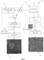
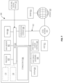
- FIG. 1 illustrates a charged particle detector system 100 in accordance with one example of the present disclosure.
- the charged particle detector system 100 of FIG. 1 can be used in conjunction with charged particle imaging systems such as the example system illustrated and described with respect to FIG. 5 .
- the charged particle detector system includes an active pixel control sensor 102 having a number of pixels, a first readout circuit 110, and a second readout circuit 130. When a charged particle strikes a pixel in the active pixel control sensor 102, one or more electron-hole pairs are generated as described in more detail below with respect to FIG. 3 .
- the first readout circuit 110 receives a unidimensional data signal corresponding to one or more electrons or holes from a sensor layer 104 of the active pixel control sensor 102 and processes the unidimensional data signal to produce unidimensional data.
- Unidimensional data can include, for example, data suitable to generate an image of the surface topology or height of features on the sample.
- the second readout circuit 130 receives a multidimensional data signal corresponding to the other of the holes or electrons (i.e., the one not used by the first readout circuit 110) from the readout chip 106 of the active pixel control sensor 102 and processes the multidimensional data signal to produce multidimensional data.
- Multidimensional data can include, for example, data suitable to generate images illustrating structural characteristics of the sample such as crystallographic phase.
- the charged particle detector system 100 produces unidimensional data signals and multidimensional data signals that are co-registered in space, co-registered in time (i.e., contemporaneous), or co-registered in both space and time.
- the active pixel control sensor 102 can have sensitivity sufficient to enable measurement of single charged particle detection events.
- the active pixel control sensor 102 can be a hybrid pixel array detector (HPAD), a segmented photodiode such as a segmented silicon photodiode, a monolithic active pixel sensor (MAPS), or any other suitable sensor with individual pixel control.
- the active pixel control sensor 102 detects strikes from charged particles such as electrons and ion and does not interact with photons.
- the active pixel control sensor 102 can include a number of pixels in a range from 32,000 to 1,000,000 pixels or in a range from 32,000 to 250,000 pixels.
- a surface of the active pixel control sensor 102 can have a length or width in a range from 10 to 40 millimeters or in a range from 20 to 30 millimeters.
- the pixels can be arranged in a rectangular or square array (e.g., 256 by 256 or 500 by 500), a circular array, or other suitable arrangements to receive charged particles or electromagnetic radiation scattered, emitted, or transmitted from a sample.
- a pitch of the pixels in an array in the active pixel control sensor 102 can be in a range from 50 to 200 microns or in a range from 50 to 150 microns. In some examples, the pitch can be 55 microns.
- an array of contiguous pixels in the active pixel control sensor 102 provides an advantage over the use of an array of photomultiplier tubes (PMTs).
- PMTs photomultiplier tubes
- Contiguous pixels avoid this issue because pixels can be placed quite close together, thus ensuring that there are no, or almost no, gaps between pixels where charged particles could be missed.
- the first readout circuit 110 receives a unidimensional data signal from the sensor layer 104 of the active pixel control sensor 102 and outputs unidimensional data (e.g., topographical imaging data) to a first computing device 112 for analysis or display.
- the first readout circuit 110 can include a current mirror 114, a bias voltage source 118, an amplifier 116, and a scanning and acquisition engine 120.
- the current mirror 114 receives the unidimensional data signal from the active pixel control sensor 102 and generates two identical data signals as outputs.
- the imaging signal can include a summation of charges generated in all or a portion of the pixels in the sensor layer 104.
- One of the unidimensional data signals output by the current mirror 114 is received at the bias voltage source 118.
- the bias voltage source 118 maintains a voltage differential across the active pixel control sensor 102 to deplete the bulk sensor volume of free charge carriers and to drive movement of electrons and holes generated within the sensor layer 104 due to the passage of charged particles.
- One of the unidimensional data signals output by the current mirror 114 is received at an amplifier 116.
- the amplifier magnifies the unidimensional data signal before passing the unidimensional data signal to the scanning and acquisition engine 120 (also referred to in some instances as the patterning imaging acquisition module or PIA).
- the scanning and acquisition engine 120 can digitize the imaging signal and also can provide control of the amplifier 116.
- the scanning and acquisition engine 120 includes one or more analog-to-digital converters.
- the scanning and acquisition engine 120 passes the digitized unidimensional data to the first computing device 112.
- the first computing device 112 collects unidimensional data for each point and assembles the unidimensional data into an intensity image 122 of the region of interest of the sample.
- the scanning and acquisition engine 120 can control operational parameters of the amplifier 116 such as by setting or controlling gain, offset, or bandwidth of the amplifier 116.
- the second readout circuit 130 receives the multidimensional data signal from a readout chip 106 of the active pixel control sensor 102 and decodes the multidimensional data signal to form multidimensional data.
- the multidimensional data is sent from the second readout circuit 130 to the second computing device 134.
- the second readout circuit 130 can include a field programmable gate array 132 (or FPGA).
- the readout chip 106 is interconnected with each pixel of the sensor layer 104 in the active pixel control sensor 102 and can readout a multidimensional data signal corresponding to the generation of holes in each of the pixels of the active pixel control sensor 102.
- the multidimensional data signal can be a two-dimensional array of intensity values where the x-y position of elements of the array represents pixel position within the active pixel control sensor 102.
- the readout chip 106 outputs the digitized multidimensional data signal to the field programmable gate array 132.
- the field programmable gate array 132 controls operation of the readout chip 106 in some examples.
- the field programmable gate array 132 can set parameters such as energy threshold values or control the master clock of the readout chip 106 as described in greater detail below.
- the FPGA 132 can control pixel analog amplifier behavior in the readout chip 106 such as discharge current and offset, hysteresis control for a comparator circuit in the readout chip 106, and conditions for communication drivers.
- the FPGA 132 can manage acquisition shutter and mode, pixel masking, and individual threshold adjustments in some examples.
- the field programmable gate array 132 can decode the multidimensional data signal to form multidimensional data.
- the multidimensional data is then transferred from the field programmable gate array 132 to the second computing device 134.
- the second computing device 134 processes the multidimensional data to produce a structural image 136.
- the structural image 136 is overlayed, composited, or otherwise combined with the intensity image 122.
- the unidimensional data signal corresponds to electrons generated within the active pixel control sensor 102 while the multidimensional data signal corresponds to holes generated within the active pixel control sensor 102. It will be understood that the systems and methods taught herein are not so limited and that the unidimensional data signal can correspond to holes generated within the active pixel control sensor 102 while the multidimensional data signal corresponds to electrons generated within the active pixel control sensor 102.
- readout of the unidimensional data signal corresponding to electrons from the sensor layer 104 is faster than readout of multidimensional data signal corresponding to holes from the readout chip 106.
- the speed to readout the full frame (i.e., signal accumulated in all pixels over a given time) for the unidimensional data signal can be in a range from 100 nanoseconds to 30 microseconds while the speed to readout the full frame for the multidimensional data signal can be in a range from 10 microseconds to 1 second.
- the speed of full-frame readout of the multidimensional data can be slower than the speed of readout of the unidimensional data for several reasons. In some instances, the additional processing overhead involved in handling the multidimensional data signal introduces delay.
- the acquisition time and/or dwell time of the exciting particle beam at the impact point 203 is increased to ensure a sufficient signal-to-noise level in each bin (e.g., individual pixels) for the multidimensional data signal.
- the unidimensional data signal can thus be faster if signal from all bins is summed and signal-to-noise ratio is thus improved.
- the unidimensional data output by the first readout circuit 110 is processed by the first computing device 112 to produce images of the surface topography of a sample.
- the unidimensional data signal output by the first readout circuit 110 is processed by the first computing device 112 to produce Z-contrast maps of the surface of the sample, i.e., images of a region of interest where the pixel color identifies a height above baseline of a corresponding location within the region of interest.
- the multidimensional data output by the second readout circuit 130 is processed by the second computing device 134 to produce images of the region of interest containing crystallographic information.
- the pixel color in the image can identify a crystallographic phase or orientation of a corresponding location in the region of interest.
- the crystallographic information in the image can be conveyed using false color or intensity maps.
- the crystallographic information can include information about how many charged particles were received from the corresponding location, information about how good the pattern is, or information about how well the pattern was indexed.
- the first computing device 112 and the second computing device 134 are separate computing devices that can be co-located or remotely situated.
- the first computing device 112 and the second computing device 134 can be connected via a network that enables information transfer between the devices.
- the first computing device 112 is a computing system attached to the charged particle microscope while the second computing device 134 is a dedicated computing system for data analysis and visualization.
- the first computing device 112 and the second computing device 134 are a same computing device. Further examples of appropriate computing devices for use with the systems and methods taught herein are described below with respect to FIG. 7 .
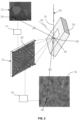
- FIG. 2 illustrates an example procedure to obtain both a structural image 136 and an intensity image 122 of a region of interest (ROI) 204 acquired using the charged particle detector system 100 of FIG. 1 .
- This example illustrates an arrangement of elements appropriate for performing electron backscatter diffraction (EBSD) measurements.
- EBSD electron backscatter diffraction
- FIG. 6A-FIG. 6C While particular examples are described herein in the context of an electron beam, it will be understood that the systems and methods taught herein are not limited to the use of electron beams but are equally applicable to a variety of charged particle beams such as beams of ions.
- a charged particle beam 228 (such as an electron beam) irradiates a sample 202 along an emission axis 201.
- the charged particle beam 228 impinges the sample 202 at impact point 203 within the ROI 204 of the sample surface.
- the impact point 203 can be a volume of the sample 202 that the irradiated elections interact with. Multiple impact points are located within the ROI. Herein, only impact point 203 is shown as an example.
- the sample 202 is positioned at a fixed angle relative to the emission axis 201 during irradiation of the sample 202 and acquisition of data.
- the sample axis 207 which is normal to the sample surface, can be positioned 70 degrees relative to the emission axis 201, so that the beam impinges the sample surface at a shallow angle of 20 degrees.
- the angle between the sample axis 207 and the emission axis 201 can be less than 45 degrees. While the impact point 203 is irradiated by the charged particle beam 228, backscatter electrons from the impact point 203 are detected by the active pixel control sensor 102.
- a two-dimensional electron backscatter pattern 205 is formed on the pixels of the active pixel control sensor 102 by the backscattered electrons from impact point 203.
- the two-dimensional electron backscatter pattern 205 is transmitted as a multidimensional data signal from the active pixel control sensor 102 to the second readout circuit 130.
- the second readout circuit 130 alone or in concert with the second computing device 134, can analyze the multidimensional data signal to determine information such as crystal orientation or crystallographic phase at the impact point 203.
- the crystal orientation can be calculated from the measured Kikuchi bands in the electron backscatter pattern 205.
- the crystal orientation is determined by matching known electron backscatter patterns (or simulated versions thereof) with the observed electron backscatter pattern 205.
- the crystal orientation is calculated by comparing the measured angles between the Kikuchi bands with theoretical interplanar angles determined using standard crystallographic principles.
- the second computing device 134 can generate and/or display a structural image 136 in the form of a crystallographic orientation image wherein the crystal orientation of the sample at impact point 203 is color-coded and shown as pixel 206 in the structural image 136.
- a structural image 136 in the form of a crystallographic orientation image wherein the crystal orientation of the sample at impact point 203 is color-coded and shown as pixel 206 in the structural image 136.
- each pixel of the structural image 136 is generated.
- Each pixel of the structural image 136 corresponds to one impact point 203 in the ROI 204, as indicated by arrow 232.
- the active pixel control sensor 102 also produces a unidimensional data signal based upon the electron backscatter pattern 205 that is transmitted to the first readout circuit 110.
- the unidimensional data signal is a summation or combination of signals from all pixels into a single intensity value.
- the unidimensional data signal can be proportional to the total flux of charged particles (such as backscattered electrons) that have impinged upon the active pixel control sensor 102.
- the unidimensional data signal is processed by the first readout circuit 110, alone or in conjunction with the first computing device 112, to produce the intensity image 122.
- a pixel 234 of the intensity image 122 can correspond to the magnitude of the unidimensional signal.
- each pixel of the intensity image 122 is generated.
- Each pixel of the intensity image 122 corresponds to one impact point 203 in the ROI 204, as indicated by the arrow 230.
- the charged particle detector system 100 increases the functionality of the active pixel control sensor 102 by enabling the active pixel control sensor 102 to act as both a structural (e.g., materials or crystallographic) imaging sensor and an intensity imaging sensor.
- a structural imaging sensor e.g., materials or crystallographic
- an intensity imaging sensor e.g., separate intensity imaging sensors
- separate secondary detectors such as forward scatter detectors (FSD) are employed that surround a primary detector such as a pixelated detector.
- the FSDs collect unidimensional data while the pixelated detector collects multidimensional data.
- the size of the FSDs is limited and is generally less than the size of the pixelated detector because of limited working space within the vacuum chamber of the instrument.
- the charged particle detector system 100 taught herein can effectively use the active pixel control sensor 102 as a virtual diode to collect unidimensional data over a large footprint (i.e., the surface of the detector, which can be of the order of 100-2000 mm 2 ). Because the surface of the active pixel control sensor 102 is larger than typical secondary detectors such as FSDs, the active pixel control sensor 102 gathers a greater number of scattered charged particles and thus exhibits improved signal-to-noise as compared to conventional secondary detectors.
- the charged particle detector system 100 taught herein can be used to more quickly locate an appropriate or desired ROI 204 by using information from both the unidimensional data signal and the multidimensional data signal.
- the first readout circuit 110 and first computing device 112 can produce intensity images 122 to orient the user in a live view.
- Live intensity images 122 can be produced simultaneously or alternately with crystallographic structural images 136 prepared by the second readout circuit 130 and second computing device 134.
- the user can identify the portion of the sample containing either topographical structures of interest or crystallographic phases of interest to help the user define an appropriate ROI 204 for further study.
- EBSD data acquisition for all impact points 203 in the ROI 204 can take minutes or hours to complete. During this long acquisition time, the sample may drift due to thermal or mechanical changes in the system.
- unidimensional data signals can be processed by the first readout circuit 110 intermittently throughout acquisition of a large multidimensional data set to enable drift correction.
- one or several multifunctional data signals are obtained from the active pixel control sensor 102 by the second readout circuit 130, each corresponding to illumination of a different impact point 203 by the charged particle beam 228. Then, the charged particle beam 228 is quickly scanned over the entire ROI 204 to produce unidimensional data signals that enable reconstruction of a full intensity image 122 of the ROI 204. If features of the sample in the ROI 204 have shifted in the intensity image 122, a drift correction can be applied to the previously obtained or subsequently obtained multidimensional data signals corresponding to individual impact points 203.
- the charged particle beam 228 can be scanned over the sample during acquisition of data signals for a single image frame.
- the charged particle beam 228 scans continuously and the signal received at the active pixel control sensor 102 is gradually improved over time after each scan of the ROI 204. Examples of this methodology that are compatible with the charged particle detector system 100 taught herein are described in U.S. Patent 11,114,275, granted September 7, 2021 and entitled "Methods and systems for acquiring electron backscatter diffraction patterns," the entire contents of this application being incorporated herein by reference.
- the charged particle detector system 100 taught herein can advantageously provide seamless drift correction during single-frame multidimensional data acquisition while scanning the beam.
- the charged particle detector system 100 enables simultaneous acquisition of multidimensional data signals and unidimensional data signals whereby the unidimensional data signals can provide drift information that can be used to correct the multidimensional data signals acquired at the same time.
- a controller or computer system can compare the intensity image and the structural image and determine a drift magnitude and direction by comparing the location of features in the two images.
- the computer system can then apply a beam shift (i.e., shifting the probe beam to a new location) and can resume or begin further data acquisition.
- the drift correction can be applied during post-processing of the images to ensure alignment of images.
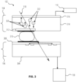
- FIG. 3 illustrates a side cross-sectional view of a single pixel in the active pixel control sensor 102 according to some examples described herein.
- the active pixel control sensor 102 includes the sensor layer 104 and the readout chip 106.
- the sensor layer 104 can include a semiconductor bulk 314 and a backside layer 316.
- the readout chip 106 can include a pixel readout layer 308 on an electronics chip 304. Segmented sections of the sensor layer 104 (i.e., single pixels) are each connected to a corresponding set of readout electronics in the readout chip 106 using, for example, bump bonding through a solder bump 310.
- the active pixel control sensor 102 is sensitive enough to discriminate single charged particle 318 events (i.e., to count the number of charged particle events per pixel during the acquisition time).
- the majority of the semiconductor bulk 314 is generally doped as p-type or n-type while an implant section 312 is doped oppositely to the majority (e.g., if the semiconductor bulk 314 is n-type, the implant section 312 is p-type).
- an implant section 312 is doped oppositely to the majority (e.g., if the semiconductor bulk 314 is n-type, the implant section 312 is p-type).
- a charged particle 318 passes through the semiconductor bulk 314, one or more electrons 320 and corresponding holes 322 are generated.
- the electrons 320 are driven towards the backside layer 316 by the applied bias voltage (e.g., applied via the bias voltage source 118 of FIG. 1 ).
- the holes 322 are driven towards the implant section 312 and through the solder bump 310.
- the holes 322 are processed by the analog and digital readout electronics in the readout chip 106 to form a digital structural signal for each pixel that can be passed to the second readout circuit 130.
- the readout electronics can include an analog frontend that connects to digital logic blocks.
- the analog frontend can include circuitry to customize detection parameters such as charge sensitive pre-amplifiers with adaptive gain mode and energy threshold discriminators (to ignore signals that fall below a predetermined energy threshold).
- the digital logic blocks digitize the amplified signal from the analog frontend.
- the digital logic blocks can also include or have access to a master clock and can thereby encode additional information into the structural signal including time of acquisition (i.e., timestamp or time duration for which the signal was received) or time over threshold (i.e., timestamp or time duration for the signal intensity was greater than a set threshold).
- time of acquisition i.e., timestamp or time duration for which the signal was received
- time over threshold i.e., timestamp or time duration for the signal intensity was greater than a set threshold
- the digital logic blocks can accept a shutter signal to control the period of time during which holes 322 are accumulated by the readout electronics for processing into the structural signal.
- the active pixel control sensor 102 can include a segmented photodiode such as a segmented silicon photodiode.
- the segmented silicon photodiode can include additional analog frontend or digital backend electronics and can, in some cases, not include energy thresholding or other signal conditioning electronics.
- the unidimensional data signal can be transmitted from the sensor layer 104 to the first readout circuit 110 through a custom connector attached to the sensor layer 104.
- the custom connector between the sensor layer 104 and the first readout circuit 110 can include a metallic line that supplies bias voltage from voltage source 118 to the backside layer 316.
- the current mirror 114 can enable bias voltage to be applied to the backside layer 316 while simultaneously allowing electrical current induced by the charged particle 318 to flow to amplifier 116.
- the current mirror 114 can include a physical connector such as an SMA connector that acts as a signal splitter.
- the charged particle 318 is produced by interactions between the sample and a charged particle beam.
- the charged particle 318 can include back-scattered electrons, Auger electrons, secondary electrons, inelastically scattered electrons (i.e., for energy loss spectroscopy), elastically scattered electrons, or variants of the above involving ions rather than electrons.
- the sensor layer 104 depicted in FIG. 3 includes a semiconductor bulk 314 that directly detects charged particle strikes
- the sensor layer 104 can include one more scintillator layers coupled with photoamplifier and/or photoelectron layers.
- the sensor layer 104 can thereby detect radiation emitted, scattered, or transmitted from the sample such as cathodoluminescence photons or x-rays (e.g., for energy dispersive spectroscopy or EDS).
- EDS energy dispersive spectroscopy
- the sensor layer 104 can include scintillators and/or particle detectors that interact with charged particles to produce light that is then converted into an electron-hole pair within a portion of the sensor layer.
- Sensor layers 104 with other activation mechanisms or pathways as known to those skilled in the art are also compatible with the systems described herein.
- a speed of data readout from the first readout circuit 110 of the active pixel control sensor 102 is greater than a speed of data readout from the second readout circuit 130. Because the structural signal includes information on signal magnitude per pixel, gathering and processing the data for output as a structural signal using the readout chip 106 can occur more slowly than reading out the imaging signal, which is proportional to the total charge in all pixels.
- Readout of the active pixel control sensor 102 to the first readout circuit 110 and the second readout circuit 130 can be simultaneous in some examples.
- an electron back-scatter diffraction implementation can use the active pixel control sensor 102 to output diffraction data from the second readout circuit 130 at the same that imaging of the specimen is performed using imaging data from the first readout circuit 110.
- a thickness of the semiconductor bulk 314 can be in a range of 50 micrometers to 1 millimeter or in a range from 300 micrometers to 500 micrometers.
- doping of the semiconductor bulk 314 and the implant section 312 can be reversed and bias voltage source 118 can be arranged oppositely to cause electrons 320 to flow downwards through the solder bump 310 while holes 322 travel upwards to the backside layer 316.
- FIG. 4A-FIG. 4F illustrate experimental images obtained using the charged particle detector system 100 of the present disclosure at different dwell times.
- a charged particle beam e.g., electron beam of a scanning electron microscope
- unidimensional and multidimensional data signals are generated by impact of scattered charged particles (e.g., electrons) on the active pixel control sensor 102.
- Unidimensional data from the active pixel control sensor 102 that is processed by the first readout circuit 110 can be used by the user to perform assistive operations such as to assess or adjust the location of the region of interest on the sample, to estimate detector background, to assess whether detector settings need to be automatically or manually adjusted, or to correct for drift occurring during acquisition.
- FIG. 4A through FIG. 4F shows a real-space image generated from unidimensional signals processed by the first readout circuit 110.
- the dwell time for each point in the region of interest is 30 microseconds, and the features of the sample in the region of interest are clearly identifiable. The dwell time is reduced to 5 microseconds in FIG. 4B , 1 microsecond in FIG. 4C , 500 nanoseconds in FIG.
- FIG. 4D 300 nanoseconds in FIG. 4E , and finally 200 nanoseconds in FIG. 4F .
- the dwell time is reduced, the amount of noise in the image increases and contrast is reduced.
- surface features of the sample are still sufficiently visible in FIG. 4F (using a dwell time of 200 nanoseconds) to enable the user to perform assistive operations.
- an example charged particle imaging system 600 is illustrated that can be used for acquiring images using various imaging modalities according to the present disclosure.
- the components of the charged particle imaging system 600 are appropriate for use as a scanning electron microscope (SEM), but the skilled person in the art would appreciate that components could be substituted are augmented as appropriate to convert the charged particle imaging system 600 into a focused ion-beam (FIB), dual-beam, or other charged particle microscope system.
- the charged particle imaging system 600 can include a charged particle beam column 610 placed on a sample chamber 620.
- the charged particle beam column 610 includes an electron source 602 for producing a beam of energetic particles (such as electrons or ions) with a selectable energy of, for example, between 500 eV and 30 keV, along emission axis 604.
- the charged particle beam can be manipulated by lenses (606, 608, 618), deflectors (612, 614), and one or more beam limiting apertures 616 to form a finely focused spot on a sample 202.
- Both the charged particle beam column 610 and the sample chamber 620 can be connected to a high vacuum pump to evacuate the enclosed volumes.
- the sample chamber 620 can optionally comprise an airlock 622 for introducing the sample therein and placing the sample on a sample holder 624.
- the sample holder 624 can rotate or translate/shift the sample so that the ROI on the sample surface can be irradiated by the finely focused electron beam under a selectable tilt angle.
- the sample chamber 620 further includes one or more detectors for receiving particles emitted from the sample.
- the active pixel control sensor 102 can be located at different positions within the sample chamber 620 to accommodate different imaging modalities. In FIG.
- each of these positions for the active pixel control sensor 102 are shown in a single image although in most examples only one active pixel control sensor 102 is employed at one of the positions.
- additional active pixel control sensors 102 can be placed inside the sample chamber 620 at different locations to enable one charged particle imaging system 600 to obtain data from multiple imaging modalities.
- the charged particle imaging system 600 could include the active pixel control sensor 102 at one location as shown in FIG. 5 while conventional sensors are located at one or more of the other locations.
- the sample can be positioned at different angles relative to the emission axis 604 to acquire different images of the sample.
- a SEM image can be acquired when the active pixel control sensor 102 is located at a first position 628 by positioning the surface of the sample 202 facing the incident beam. That is, a sample axis is aligned with the emission axis 604.
- EBSD patterns can be acquired when the active pixel control sensor 102 is located at a second position 626 by positioning the sample 202 at an angle of about 70 degrees relative to the emission axis 604.
- EBSD patterns can be acquired (e.g., utilizing reflected Kikuchi diffraction) when the active pixel control sensor 102 is at the third position 632 by positioning the sample 202 at an angle of less than 45 degrees relative to the emission axis 604.
- the SEM image can also be acquired by positioning the sample at an angle relative to the emission axis.
- the active pixel control sensor 102 can be located at a fourth position 634 to detect x-rays for EDS analysis.
- the voltages and/or currents needed for the working of the (magnetic or electrostatic) lenses and of the electron source are generated/controlled by a column controller 636, while a computing device 630 generates deflection signals for the deflectors and processes data from the first readout circuit 110 or the second readout circuit 130.
- the computing device 630 can be a computing device such as the first computing device 112 or second computing device 134 in some examples or can act as both the first computing device 112 and the second computing device 134.
- the computing device 630 can be connected to a display 638 for displaying information, such as an image of the sample 202.
- the computing device 630 can also receive operator inputs from the input device 640.
- the input device 640 can be a mouse, a keyboard, or a touchpad.
- the controller can translate, shift, or tilt the sample relative to the incident beam by moving the sample holder 624.
- the computing device 630 can scan the sample with the charged particle beam by adjusting the beam via the deflector 612 and/or deflector 614.
- the computing device 630 is configured to process data received from the first readout circuit 110 or second readout circuit 130 and can thereby reconstruct, for example, an SEM image, EBSD patterns or crystallographic orientation image of the sample.
- the computing device 630 can include one or more field-programmable gate arrays (FPGA) configured to process data from the first readout circuit 110 or the second readout circuit 130 or signals from other secondary detectors installed in the charged particle imaging system 600.
- FPGA field-programmable gate arrays
- the imaging system can be other types of charge-particle microscopy system, such as transmission electron microscopy (TEM), scanning transmission electron microscopy (STEM), or a dual beam tool such as a focused ion beam combined with scanning electron microscopy (FIB-SEM).
- TEM transmission electron microscopy
- STEM scanning transmission electron microscopy
- FIB-SEM scanning electron microscopy
- the present discussion of the SEM system is provided merely as an example of one suitable imaging system for acquiring backscattered electrons.
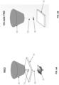
- FIG. 6A illustrates the detector arrangement for a reflected Kikuchi diffraction (RKD) imaging modality in accordance with some examples described herein.
- the active pixel control sensor 102 is placed between the sample 202 and the final elements of the charged particle beam column represented in this figure as a column lens 702.
- the active pixel control sensor 102 includes a hole or aperture 718 through which the charged particle beam 228 passes on its way to the sample 202.
- two or four active pixel control sensors 102 can be tiled together with an appropriate gap between them to allow the charged particle beam 228 to pass through unimpeded.
- charged particles e.g., electrons or ions
- the active pixel control sensor 102 is oriented so that the sensor layer 104 is facing the sample 202 below, i.e., the sensor layer 104 is on the opposite side of the active pixel control sensor 102 from the column lens 702.
- Multidimensional data collected in an RKD experiment can be used to identify structural information about the sample such as crystallographic phase or orientation.
- the presence of the RKD detector (for example, a concentric backscatter (CBS) detector or a directional backscatter (DBS) detector) often interferes with the separate imaging detectors as the RKD detector blocks or reduces signal to the imaging detectors when inserted.
- CBS concentric backscatter
- DBS directional backscatter
- the use of the present charged particle detector system 100 in RKD imaging is particularly advantageous as there is no need to move or remove the backscatter RKD detector to enable the use of the imaging detector as is usually done in conventional systems.
- the charged particle detector system 100 enables the user to obtain back-scattered electron (BSE) images of the sample surface at sufficiently fast speed (e.g., at timescales of tens of microseconds or less) to considerably decrease the time needed to locate the region of interest.
- BSE back-scattered electron
- the possibility of simultaneous output of unidimensional data signal and multidimensional data signal enables the collection of background levels of the multidimensional data signal during the time that the user is searching for the region of interest by referring to images generated from the unidimensional data signal. The background levels collected during location adjustment can then be used during processing of subsequent multidimensional data signals at the desired region of interest, thus reducing total acquisition time.
- the unidimensional data signal for each active pixel control sensor 102 can be readout separately (e.g., using separate first readout circuits 110) or the unidimensional data signal from all active pixel control sensors 102 can be read out collectively (e.g., through a single first readout circuit 110).
- the unidimensional data output from each individual first readout circuit 110 can be compared or combined to produce images with differential contrast, i.e., orientation, atomic density, or topographical contrast.
- FIG. 6B illustrates the detector arrangement for an on-axis transmitted Kikuchi diffraction (TKD) imaging modality or a four-dimensional scanning transmission electron microscopy (4-D STEM) imaging modality in accordance with some examples described herein.
- the active pixel control sensor 102 is placed behind the sample 202 and receives charged particles that are scattered, reflected, emitted, or transmitted through the sample 202 on substantially the same axis as the charged particle beam 228 after interaction of the charged particle beam 228 with the sample 202.
- the active pixel control sensor 102 can output both a unidimensional data signal and a multidimensional data signal to enable reconstruction of both a direct image of the field of view (e.g., a density contrast image similar to that obtained by a transmission electron microscope) and a structural image of the field of view where structural information about each location in the field of view (e.g., crystallographic phase or orientation) is represented in the image.
- a direct image of the field of view e.g., a density contrast image similar to that obtained by a transmission electron microscope
- structural image of the field of view where structural information about each location in the field of view (e.g., crystallographic phase or orientation) is represented in the image.
- FIG. 6C illustrates the detector arrangement for an off-axis transmitted Kikuchi diffraction (TKD) imaging modality in accordance with some examples described herein.
- the active pixel control sensor 102 is placed behind the sample 202 and receives charged particles that are scattered, reflected, emitted, or transmitted through the sample 202 at an angle with respect to the axis of the charged particle beam 228 after interaction of the charged particle beam 228 with the sample 202.
- the active pixel control sensor 102 is positioned to receive particles from the sample 202 at an angle of about 70° with respect to the transmission axis of the charged particle beam 228.
- the active pixel control sensor 102 can output both a unidimensional data signal and a multidimensional data signal to enable reconstruction of both a direct image of the field of view (e.g., a density contrast image similar to that obtained by a transmission electron microscope) and a structural image of the field of view where structural information about each location in the field of view (e.g., crystallographic phase or orientation) is represented in the image.
- a direct image of the field of view e.g., a density contrast image similar to that obtained by a transmission electron microscope
- structural image of the field of view where structural information about each location in the field of view (e.g., crystallographic phase or orientation) is represented in the image.
- FIG. 7 is a block diagram that illustrates a computing device 800 that are appropriate for use with examples as taught herein.
- the computing device 800 can operate as the first computing device 112 or second computing device 134 as described above or can perform functions of both the first computing device 112 and the second computing device 134.
- the computing device 800 can be an example of computing hardware included with charged particle detector system 100 such as the first computing device 112 or the second computing device 134.
- Computing device 800 at least includes a bus 810 or other communication mechanism for communicating information, and one or more processors 820 coupled with bus 810 for processing information.
- the processor 820 can be, for example, a general-purpose microprocessor or other hardware processor.
- the computing device 800 can be used to implement the methods and techniques disclosed herein, such as method 900.
- Computing device 800 also includes a main memory 802, such as a random-access memory (RAM) or other dynamic storage device, coupled to bus 810 for storing information and instructions to be executed by processor 820.
- Main memory 802 also can be used for storing temporary variables or other intermediate information during execution of instructions to be executed by processor 820.
- Such instructions when stored in non-transitory storage media accessible to processor 820, render computing device 800 into a special-purpose machine that is customized to perform the operations specified in the instructions.
- Computing device 800 can further include a read-only memory 804 (ROM) or other static storage device coupled to bus 810 for storing static information and instructions for processor 820.
- ROM read-only memory
- Computing device 800 can be coupled via bus 810 to a display 638, such as a cathode ray tube (CRT) or flat-screen display, for displaying information to a computer user.
- a display 638 such as a cathode ray tube (CRT) or flat-screen display
- An input device 640 is coupled to bus 810 for communicating information and command selections to processor 820.
- cursor control such as a mouse, a trackball, a touchscreen, or cursor direction keys for communicating direction information and command selections to processor 820 and for controlling cursor movement on display 638.
- This input device typically has two degrees of freedom in two axes, a first axis (e.g., x) and a second axis (e.g., y), that allows the device to specify positions in a plane.
- first readout circuit 110, the second readout circuit 130, or both the first readout circuit 110 and the second readout circuit 130 can be physically housed within the computing device 800.
- the readout circuits can be implemented on printed circuit boards that are inserted into a housing that houses one or more of the other components of the computing device 800. This arrangement is optional as the first readout circuit 110, second readout circuit 130, or both circuits can be implemented as standalone units in other examples.
- the first readout circuit 110 and second readout circuit 130 can connect to the bus 810 of the computing device 800 to enable data transfer and analysis by the processor 820.
- the active pixel control sensor 102 can connect directly to the first readout circuit 110 or second readout circuit 130 or can connect through the bus 810 to the first readout circuit 110 or the second readout circuit 130.
- Computing device 800 can implement the techniques described herein using customized hard-wired logic, one or more application specific integrated circuits (ASICs) or field-programmable gate arrays (FPGAs), firmware and/or program logic which in combination with the computer system causes or programs computing device 800 to be a special-purpose machine.
- the techniques herein are performed by computing device 800 in response to processor 820 executing one or more sequences of one or more instructions contained in main memory 802. Such instructions can be read into main memory 802 from another storage medium, such as storage device 806. Execution of the sequences of instructions contained in main memory 802 causes processor 820 to perform the process steps described herein.
- hard-wired circuitry can be used in place of or in combination with software instructions.
- Non-volatile media includes, for example, optical or magnetic disks, such as storage device 806.
- Volatile media includes dynamic memory, such as main memory 802.
- Common forms of storage media include, for example, a floppy disk, a flexible disk, hard disk, solid state drive, magnetic tape, or any other magnetic data storage medium, a CD-ROM, any other optical data storage medium, any physical medium with patterns of holes, a RAM, a PROM, and EPROM, a FLASH-EPROM, NVRAM, any other memory chip or cartridge, content-addressable memory (CAM), and ternary content-addressable memory (TCAM).
- a floppy disk a flexible disk, hard disk, solid state drive, magnetic tape, or any other magnetic data storage medium
- CD-ROM any other optical data storage medium
- any physical medium with patterns of holes a RAM, a PROM, and EPROM
- FLASH-EPROM any other memory chip or cartridge
- CAM content-addressable memory
- TCAM ternary content-addressable memory
- Storage media is distinct from but can be used in conjunction with transmission media.
- Transmission media participates in transferring information between storage media.
- transmission media includes coaxial cables, copper wire and fiber optics, including the wires that comprise bus 810.
- transmission media can also take the form of acoustic or light waves, such as those generated during radio-wave and infra-red data communications.
- Various forms of media can be involved in carrying one or more sequences of one or more instructions to processor 820 for execution.
- the instructions can initially be carried on a magnetic disk or solid-state drive of a remote computer.
- the remote computer can load the instructions into its dynamic memory and send the instructions over a telephone line using a modem.
- a modem local to computing device 800 can receive the data on the telephone line and use an infra-red transmitter to convert the data to an infra-red signal.
- An infra-red detector can receive the data carried in the infra-red signal and appropriate circuitry can place the data on bus 810.
- Bus 810 carries the data to main memory 802, from which processor 820 retrieves and executes the instructions.
- the instructions received by main memory 802 can optionally be stored on storage device 806 either before or after execution by processor 820.
- Computing device 800 can also include a communication interface 808 coupled to the bus 810.
- the communication interface 808 provides a two-way data communication coupling the computing device 800 to a network link 822 that is connected to a local network 814.
- communication interface 808 can be an integrated services digital network (ISDN) card, cable modem, satellite modem, or a modem to provide a data communication connection to a corresponding type of telephone line.
- ISDN integrated services digital network
- communication interface 808 can be a local area network (LAN) card to provide a data communication connection to a compatible LAN.
- LAN local area network
- Wireless links can also be implemented.
- communication interface 808 sends and receives electrical, electromagnetic or optical signals that carry digital data streams representing various types of information.
- the network link 822 typically provides data communication through one or more networks to other data devices.
- network link 822 can provide a connection through local network 814 to a host computer 812 or to data equipment operated by an Internet Service Provider (ISP) that provides data communication services through the worldwide packet data communication network now commonly referred to as the internet 818.
- ISP Internet Service Provider
- Local network 814 and internet 818 both use electrical, electromagnetic or optical signals that carry digital data streams.
- the signals through the various networks and the signals on network link 822 and through communication interface 808, which carry the digital data to and from computing device 800, are example forms of transmission media.
- Computing device 800 can send messages and receive data, including program code, through the network(s), network link 822 and communication interface 808.
- a server 816 might transmit a requested code for an application program through the internet 818, local network 814 and/or communication interface 808.
- the received code can be executed by processor 820 as it is received, and/or stored in storage device 806, and/or stored in other volatile or non-volatile storage for later execution.
- FIG. 8 illustrates an example method 900 for imaging a sample according to examples taught herein.
- the example method 900 depicts a particular sequence of operations, the sequence can be altered without departing from the scope of the present disclosure. For example, some of the operations depicted can be performed in parallel or in a different sequence that does not materially affect the function of the method 900. In other examples, different components of an example device or system that implements the method 900 can perform functions at substantially the same time or in a specific sequence.
- the method 900 includes directing a charged particle beam to a location in a region of interest on a sample (block 904).
- the charged particle imaging system 600 described above can direct a charged particle beam 228 to the impact point 203 in the ROI 204 of the sample 202.
- the method 900 also includes receiving, at pixels of an active pixel control sensor 102, charged particles that are emitted, scattered, or transmitted from the location (block 906).
- the active pixel control sensor 102 can be placed inside the sample chamber 620 at a location (e.g., the first position 628, the second position 626, the third position 632, the fourth position 634, or other suitable positions) such that it can receive charged particles resulting from the interaction of the charged particle beam 228 with the sample 202.
- a location e.g., the first position 628, the second position 626, the third position 632, the fourth position 634, or other suitable positions
- the method 900 then splits into two parallel pathways. These pathways can be performed in parallel (i.e., contemporaneously) or at different times.
- the method 900 includes transmitting a unidimensional data signal corresponding to one of electrons or holes generated in the active pixel control sensor 102 to a first readout circuit 110 (block 908).
- the unidimensional data signal is transferred from the sensor layer 104 to the first readout circuit 110.
- the method 900 also includes generating unidimensional data from the unidimensional data signal using the first readout circuit 110 (block 910).
- the method 900 also includes generating a pixel in a first image by processing unidimensional data from the first readout circuit 110 (block 912).
- the first image can be an intensity image 122.
- the method 900 includes transmitting multidimensional data signal corresponding to the other of electrons or holes generated in the active pixel control sensor to a second readout circuit 130 (block 914).
- the multidimensional data signal is transferred from the readout chip 106 to the second readout circuit 130.
- the method 900 also includes generating multidimensional data from the multidimensional data signal using the second readout circuit 130.
- the method 900 also includes generating a pixel in a second image by processing multidimensional data from the second readout circuit 130 (block 918).
- the second image can be a structural image 136.
- the method 900 includes selecting a new location within the region of interest to illuminate (block 920). The method 900 can then be iterated to generate further pixels in the first or second images until all of the locations within the region of interest have been illuminated by the charged particle beam. It will be understood that both pathways may not be performed in each iteration in some examples.
- the first pathway may be performed in a number of iterations to produce a complete intensity image by using a short dwell time (e.g., hundreds of nanoseconds) of the charged particle beam at the location on the sample to quickly assemble the intensity image 122.
- the second pathway can be performed one or a number of times to gather multidimensional data at a longer dwell time of the charged particle beam at the location to improve signal-to-noise ratio.
- the multidimensional data gathering may be interrupted or interspersed with unidimensional data gathering at short dwell time to prepare an intensity image or otherwise determine if the sample location has drifted. Drift corrections can then be applied to the multidimensional data.
- a complete structural image 136 and corresponding intensity image 122 can be generated from signals produced by a single active pixel control sensor 102.
- FIG. 9 illustrates an example method 1000 for assembling a charged particle detector system as taught herein.
- the example method 1000 depicts a particular sequence of operations, the sequence may be altered without departing from the scope of the present disclosure. For example, some of the operations depicted may be performed in parallel or in a different sequence that does not materially affect the function of the method 1000. In other examples, different components of an example device or system that implements the method 1000 may perform functions at substantially the same time or in a specific sequence.
- the method 1000 includes providing an active pixel control sensor 102 having a sensor layer 104 and a readout chip 106 at block 1002.
- the method 1000 includes connecting the sensor layer 104 of the active pixel control sensor 102 to a first readout circuit 110 configured to process unidimensional data signals from the sensor layer 104 at block 1004.
- the method 1000 includes connecting the readout chip 106 of the active pixel control sensor 102 to a second readout circuit 130 configured to process multidimensional data signals from the readout chip 106 at block 1006.
- the method 1000 includes connecting a first computing device 112 to the first readout circuit 110 to generate intensity images 122 of a sample 202 from unidimensional data provided by the first readout circuit 110 at block 1008.
- the method 1000 includes connecting a second computing device 134 to the second readout circuit 130 to generate structural images 136 of the sample 202 from multidimensional data provided by the second readout circuit 130 at block 1010.
- the embodiments described herein can be practiced with other computer system configurations including hand-held devices, microprocessor systems, microprocessor-based or programmable consumer electronics, minicomputers, mainframe computers and the like.
- the embodiments can also be practiced in distributing computing environments where tasks are performed by remote processing devices that are linked through a network.
- Certain embodiments can also be embodied as computer readable code on a computer readable medium.
- the computer readable medium is any data storage device that can store data, which can thereafter be read by a computer system. Examples of the computer readable medium include hard drives, network attached storage (NAS), read-only memory, random-access memory, CD-ROMs, CD-Rs, CD-RWs, magnetic tapes, and other optical and non-optical data storage devices.
- the computer readable medium can also be distributed over a network of coupled computer systems so that the computer readable code is stored and executed in a distributed fashion.
- a "system” as used herein sets forth a set of components, real or abstract, comprising a whole where each component interacts with or is related to at least one other component within the whole.
Landscapes
- Chemical & Material Sciences (AREA)
- Analytical Chemistry (AREA)
- Physics & Mathematics (AREA)
- Health & Medical Sciences (AREA)
- Life Sciences & Earth Sciences (AREA)
- Biochemistry (AREA)
- General Health & Medical Sciences (AREA)
- General Physics & Mathematics (AREA)
- Immunology (AREA)
- Pathology (AREA)
- Crystallography & Structural Chemistry (AREA)
- Analysing Materials By The Use Of Radiation (AREA)
Applications Claiming Priority (1)
| Application Number | Priority Date | Filing Date | Title |
|---|---|---|---|
| US18/545,447 US20250201511A1 (en) | 2023-12-19 | 2023-12-19 | Systems and methods for analyzing a sample using charged particle beams and active pixel control sensors |
Publications (1)
| Publication Number | Publication Date |
|---|---|
| EP4575475A1 true EP4575475A1 (fr) | 2025-06-25 |
Family
ID=93852998
Family Applications (1)
| Application Number | Title | Priority Date | Filing Date |
|---|---|---|---|
| EP24218633.6A Pending EP4575475A1 (fr) | 2023-12-19 | 2024-12-10 | Systèmes et procédés d'analyse d'un échantillon à l'aide de faisceaux de particules chargées et de capteurs à pixels actifs commandés |
Country Status (4)
| Country | Link |
|---|---|
| US (1) | US20250201511A1 (fr) |
| EP (1) | EP4575475A1 (fr) |
| JP (1) | JP2025097962A (fr) |
| CN (1) | CN120177530A (fr) |
Citations (1)
| Publication number | Priority date | Publication date | Assignee | Title |
|---|---|---|---|---|
| US11114275B2 (en) | 2019-07-02 | 2021-09-07 | Fei Company | Methods and systems for acquiring electron backscatter diffraction patterns |
Family Cites Families (5)
| Publication number | Priority date | Publication date | Assignee | Title |
|---|---|---|---|---|
| US5886353A (en) * | 1995-04-21 | 1999-03-23 | Thermotrex Corporation | Imaging device |
| US6576899B2 (en) * | 2001-01-16 | 2003-06-10 | California Institute Of Technology | Direct detection of low-energy charged particles using metal oxide semiconductor circuitry |
| US6873153B2 (en) * | 2003-07-07 | 2005-03-29 | Yeda Research And Development Co., Ltd. | Method and apparatus for acquiring multidimensional spectra and improved unidimensional spectra within a single scan |
| EP4139714A1 (fr) * | 2020-04-24 | 2023-03-01 | Carl Zeiss X-Ray Microscopy, Inc. | Système de détection de particules et de rayons x à résolution spectrale et spatiale |
| WO2022248296A2 (fr) * | 2021-05-27 | 2022-12-01 | Asml Netherlands B.V. | Manipulation du comportement de transport de porteurs dans un détecteur |
-
2023
- 2023-12-19 US US18/545,447 patent/US20250201511A1/en active Pending
-
2024
- 2024-12-10 EP EP24218633.6A patent/EP4575475A1/fr active Pending
- 2024-12-18 CN CN202411868692.1A patent/CN120177530A/zh active Pending
- 2024-12-18 JP JP2024221863A patent/JP2025097962A/ja active Pending
Patent Citations (1)
| Publication number | Priority date | Publication date | Assignee | Title |
|---|---|---|---|---|
| US11114275B2 (en) | 2019-07-02 | 2021-09-07 | Fei Company | Methods and systems for acquiring electron backscatter diffraction patterns |
Non-Patent Citations (3)
| Title |
|---|
| FARUQI ET AL: "Electronic detectors for electron microscopy", CURRENT OPINION IN STRUCTURAL BIOLOGY, ELSEVIER LTD, GB, vol. 17, no. 5, 29 October 2007 (2007-10-29), pages 549 - 555, XP022324278, ISSN: 0959-440X, DOI: 10.1016/J.SBI.2007.08.014 * |
| SCHWARZER ROBERT A ET AL: "Backscattered Electron Imaging with an EBSD Detector", MICROSCOPY TODAY, vol. 23, no. 1, 31 January 2015 (2015-01-31), pages 12 - 17, XP093268343, DOI: 10.1017/S1551929514001333 * |
| STUART I. WRIGHT ET AL: "Electron imaging with an EBSD detector", ULTRAMICROSCOPY, vol. 148, 23 October 2014 (2014-10-23), NL, pages 132 - 145, XP055763084, ISSN: 0304-3991, DOI: 10.1016/j.ultramic.2014.10.002 * |
Also Published As
| Publication number | Publication date |
|---|---|
| CN120177530A (zh) | 2025-06-20 |
| US20250201511A1 (en) | 2025-06-19 |
| JP2025097962A (ja) | 2025-07-01 |
Similar Documents
| Publication | Publication Date | Title |
|---|---|---|
| JP5801891B2 (ja) | 電子イメージングを用いて試料の画像を作成する荷電粒子線装置及び方法 | |
| JP6215202B2 (ja) | 密接に結合したシンチレータ−光電子増倍管の1又は複数の組合体を含む電子検出器及びそれを使用した電子顕微鏡 | |
| KR102454320B1 (ko) | 복수의 하전 입자 빔들을 이용하여 샘플을 검사하는 장치 및 방법 | |
| JP5698885B2 (ja) | X線分光法用の微量熱量測定 | |
| CN105551921B (zh) | 带电粒子显微镜中的复合扫描路径 | |
| EP2511937B1 (fr) | Microscope électronique | |
| JP2013541799A5 (fr) | ||
| CN103718268A (zh) | 带电粒子线装置 | |
| JP6999751B2 (ja) | 荷電粒子線デバイス用のセグメント化検出器 | |
| US6552338B1 (en) | Ion photon emission microscope | |
| CN108447758A (zh) | 带电粒子源的排放噪声校正 | |
| CN109411320A (zh) | 透射带电粒子显微镜中的衍射图案检测 | |
| JP2021018988A (ja) | 荷電粒子検出器を製造する方法 | |
| KR20230067599A (ko) | 시간-분해된 음극발광 샘플 탐색 | |
| JP7467621B2 (ja) | 分光技術のための荷電粒子検出 | |
| EP4119934B1 (fr) | Procédé et système de génération d'image de diffraction | |
| EP4575475A1 (fr) | Systèmes et procédés d'analyse d'un échantillon à l'aide de faisceaux de particules chargées et de capteurs à pixels actifs commandés | |
| CN114113686B (zh) | 用于同时相位衬度成像和电子能量损失光谱法的系统和方法 | |
| Mac Raighne et al. | Medipix2 as a highly flexible scanning/imaging detector for transmission electron microscopy | |
| EP4310884A1 (fr) | Détecteur de particules chargées pour microscopie | |
| Haidl et al. | Fast X-ray detection using a CCD for application in a scanning transmission X-ray microscope | |
| WO2025202056A1 (fr) | Système à faisceaux d'électrons multiples pour inspection avec des électrons rétrodiffusés |
Legal Events
| Date | Code | Title | Description |
|---|---|---|---|
| PUAI | Public reference made under article 153(3) epc to a published international application that has entered the european phase |
Free format text: ORIGINAL CODE: 0009012 |
|
| STAA | Information on the status of an ep patent application or granted ep patent |
Free format text: STATUS: THE APPLICATION HAS BEEN PUBLISHED |
|
| AK | Designated contracting states |
Kind code of ref document: A1 Designated state(s): AL AT BE BG CH CY CZ DE DK EE ES FI FR GB GR HR HU IE IS IT LI LT LU LV MC ME MK MT NL NO PL PT RO RS SE SI SK SM TR |
|
| STAA | Information on the status of an ep patent application or granted ep patent |
Free format text: STATUS: REQUEST FOR EXAMINATION WAS MADE |
|
| 17P | Request for examination filed |
Effective date: 20251125 |