EP4575445A1 - Optische sonde und zugehörige verfahren - Google Patents
Optische sonde und zugehörige verfahren Download PDFInfo
- Publication number
- EP4575445A1 EP4575445A1 EP24221372.6A EP24221372A EP4575445A1 EP 4575445 A1 EP4575445 A1 EP 4575445A1 EP 24221372 A EP24221372 A EP 24221372A EP 4575445 A1 EP4575445 A1 EP 4575445A1
- Authority
- EP
- European Patent Office
- Prior art keywords
- optical
- micro
- testing circuit
- probe
- light
- Prior art date
- Legal status (The legal status is an assumption and is not a legal conclusion. Google has not performed a legal analysis and makes no representation as to the accuracy of the status listed.)
- Pending
Links
Images


Classifications
-
- G—PHYSICS
- G01—MEASURING; TESTING
- G01M—TESTING STATIC OR DYNAMIC BALANCE OF MACHINES OR STRUCTURES; TESTING OF STRUCTURES OR APPARATUS, NOT OTHERWISE PROVIDED FOR
- G01M11/00—Testing of optical apparatus; Testing structures by optical methods not otherwise provided for
- G01M11/30—Testing of optical devices, constituted by fibre optics or optical waveguides
- G01M11/31—Testing of optical devices, constituted by fibre optics or optical waveguides with a light emitter and a light receiver being disposed at the same side of a fibre or waveguide end-face, e.g. reflectometers
- G01M11/3109—Reflectometers detecting the back-scattered light in the time-domain, e.g. OTDR
- G01M11/3154—Details of the opto-mechanical connection, e.g. connector or repeater
-
- G—PHYSICS
- G01—MEASURING; TESTING
- G01M—TESTING STATIC OR DYNAMIC BALANCE OF MACHINES OR STRUCTURES; TESTING OF STRUCTURES OR APPARATUS, NOT OTHERWISE PROVIDED FOR
- G01M11/00—Testing of optical apparatus; Testing structures by optical methods not otherwise provided for
- G01M11/02—Testing optical properties
- G01M11/0207—Details of measuring devices
-
- G—PHYSICS
- G01—MEASURING; TESTING
- G01M—TESTING STATIC OR DYNAMIC BALANCE OF MACHINES OR STRUCTURES; TESTING OF STRUCTURES OR APPARATUS, NOT OTHERWISE PROVIDED FOR
- G01M11/00—Testing of optical apparatus; Testing structures by optical methods not otherwise provided for
- G01M11/08—Testing mechanical properties
- G01M11/083—Testing mechanical properties by using an optical fiber in contact with the device under test [DUT]
-
- G—PHYSICS
- G01—MEASURING; TESTING
- G01M—TESTING STATIC OR DYNAMIC BALANCE OF MACHINES OR STRUCTURES; TESTING OF STRUCTURES OR APPARATUS, NOT OTHERWISE PROVIDED FOR
- G01M11/00—Testing of optical apparatus; Testing structures by optical methods not otherwise provided for
- G01M11/30—Testing of optical devices, constituted by fibre optics or optical waveguides
- G01M11/33—Testing of optical devices, constituted by fibre optics or optical waveguides with a light emitter being disposed at one fibre or waveguide end-face, and a light receiver at the other end-face
-
- G—PHYSICS
- G02—OPTICS
- G02B—OPTICAL ELEMENTS, SYSTEMS OR APPARATUS
- G02B6/00—Light guides; Structural details of arrangements comprising light guides and other optical elements, e.g. couplings
- G02B6/24—Coupling light guides
- G02B6/42—Coupling light guides with opto-electronic elements
- G02B6/4201—Packages, e.g. shape, construction, internal or external details
- G02B6/4204—Packages, e.g. shape, construction, internal or external details the coupling comprising intermediate optical elements, e.g. lenses, holograms
- G02B6/4214—Packages, e.g. shape, construction, internal or external details the coupling comprising intermediate optical elements, e.g. lenses, holograms the intermediate optical element having redirecting reflective means, e.g. mirrors, prisms for deflecting the radiation from horizontal to down- or upward direction toward a device
-
- G—PHYSICS
- G02—OPTICS
- G02B—OPTICAL ELEMENTS, SYSTEMS OR APPARATUS
- G02B6/00—Light guides; Structural details of arrangements comprising light guides and other optical elements, e.g. couplings
- G02B6/24—Coupling light guides
- G02B6/42—Coupling light guides with opto-electronic elements
- G02B6/4201—Packages, e.g. shape, construction, internal or external details
- G02B6/4249—Packages, e.g. shape, construction, internal or external details comprising arrays of active devices and fibres
Definitions
- the present invention relates to optical coupling between optical components and, more particular, to an optical probe configured for optical testing of at least one micro-optical component, to a method for producing an optical probe, and to a method for optical testing of at least one micro-optical component.
- the optical probe can be used for fabrication, calibration, testing, and preselection of micro-optical components, which are particularly configured for optical communication, sensor applications, medical sensors, automotive applications, quantum applications, or environmental sensing; however, using the optical probe in other applications is also possible.
- Optical probes which are configured for optically coupling to photonic integrated circuits featuring 3D-printed optics on fiber arrays are known. Further known are 3D-printed optics for optical packaging. Still further known are 3D-printed freeform probes for beam shaping of light exiting photonic integrated circuits.
- WO 2018/083191 A1 discloses a fabrication of micro-optics for beam expansion on photonic integrated circuits for optical packaging.
- WO 2023/132785A1 discloses an apparatus for wafer level testing of a semiconductor device comprising an optoelectronic unit, an optical interface and an optical fiber array optically coupled between the optoelectronic unit and the optical interface.
- the optoelectronic unit transmits one or more optical test signals to the semiconductor device and receives one or more optical response signals from the semiconductor device for testing at least one function of the semiconductor device.
- the optical interface optically couples the optical fiber array and the semiconductor device.
- the optical interface includes a steering element for steering the optical test signals towards the semiconductor device and the response signals towards the optical fiber array.
- US 2018/0143245 A1 discloses an integrated optical probe card and a system for performing wafer testing of optical micro-electro-mechanical systems (MEMS) structures with an in-plane optical axis.
- On-wafer optical screening of optical MEMS structures may be performed utilizing one or more micro-optical bench components to redirect light between an out-of-plane direction that is perpendicular to the in-plane optical axis to an in-plane direction that is parallel to the in-plane optical axis to enable testing of the optical MEMS structures with vertical injection of the light.
- MEMS micro-electro-mechanical systems
- EP 4 001 980 A1 discloses systems and methods for testing a photonic IC (PIC) with an optical probe having an out-of-plane edge coupler to convey test signals between the out-of-plane probe and an edge coupled photonic waveguide within a plane of the PIC.
- PIC photonic IC
- a test trench may be fabricated in the PIC near an edge coupler of the waveguide.
- the optical probe may be displaced along one or more axes relative to a prober to position a free end of the prober within the test trench and to align the probe's out-of-plane edge coupler with an edge coupler of a PIC waveguide.
- a PIC may be probed at the wafer-level, without first dicing a wafer into PIC chips or bars.
- the optical probe may be physically coupled to a prober through a contact sensor to detect and/or avoid physical contact between probe and PIC.
- WO 2022/266760 A1 and Stefan Singer et al disclose optical coupling mechanisms which form a background to the present invention.
- the optical probe should have a compact probe head that can be inserted and probe in a trench of a wafer, wherein the trench may, preferably, 250 ⁇ m or less, more preferred 100 ⁇ m or less, especially 80 ⁇ m or less.
- the optical probe should be configured for a small pitch, preferably of 127 ⁇ m or less, more preferred of 80 ⁇ m or less, especially of 50 ⁇ m or less.
- the optical probe should be configured for a high port count, preferably at least 24, more preferred at least 64, especially at least 128.
- a small mode-field preferably of 10 ⁇ m or less, more preferred of 5 ⁇ m or less, especially twice an operation wavelength or less, should be available at a coupling location of the testing circuit.
- a calibration of probe variations shall be possible.
- the optical probe should be configured for robust probing even at high working distances. In addition, achieving a high testing throughput would be preferred.
- the optical probe may implement at least one additional functionality, such as distance measurement, local probing of polarization, multiplexing, modulation, spectral analysis, intensity and phase measurements, heterodyne detection and transmittance of signals.
- the optical probe is configured for working in the near ultraviolet range, the visual range, the near infrared range, and the medium infrared range, referring to a wavelength range of 100 nm to 10 ⁇ m, preferably of 200 nm to 4 ⁇ m, more preferred 530 nm to 2 ⁇ m, especially at least 1250 nm to 1650 nm.
- a high reproducibility of the optical coupling between the probe head and the at least one micro-optical component with variations of 0.5 dB or less, more preferred of 0.25 dB or less would be preferred.
- the present invention relates to an optical probe configured for optical testing of at least one micro-optical component.
- the optical probe comprises
- the term "optical probe” refers to an optical device, which is configured for optical testing of at least one micro-optical component.
- the optical probe may exhibit at least one of a mechanical functionality, an electrical functionality, or an optical functionality as described below in more detail.
- the optical probe as used herein comprises a probe head having a testing circuit, wherein the probe head may be aligned in a manner that light may couple between the testing circuit and the micro-optical component.
- the term “probe head” refers to a terminal piece of the optical probe, wherein the terminal piece comprises a micro-optical element configured to optically couple light between the testing circuit and the micro-optical component.
- the probe head may be movable relative to the micro-optical component to be tested.
- the probe head may, preferably, exhibit a low weight.
- the optical probe is configured for the optical testing of at least one micro-optical component.
- the term "micro-optical component” refers to a device under testing, wherein the device may, preferably, be or comprise a wafer having multiple photonic integrated circuits, or individual photonic integrated circuits.
- micro-optical component may comprise a plurality of optical structures that inherently assume small dimensions, preferably of 10 ⁇ m or less, more preferred of 5 ⁇ m or less, especially of 1 ⁇ m or less, configured to execute an intended function, in particular as a waveguide or a groove of a grating, or that has a total dimension 10 mm or less.
- the micro-optical component may be produced on a photonic platform, particularly selected from a SOI (Silicon on Insulator), InP (Indium Phosphide), SiN (Silicon Nitride), or LNOI (Lithium Niobate thin film).
- the micro-optical component may be a non-planar component, especially an optical element selected from a micro-lens, a grating, an optical isolator, or a mirror.
- the optical probe comprises a probe head having a testing circuit.
- testing circuit refers to at least one photonic integrated circuit, which is configured for characterizing a performance of a micro-optical component.
- the testing circuit may, preferably, comprise the same material, fabrication batch, wafer or technology as the micro-optical element. However, using a different type of testing circuit may also be feasible.
- the testing circuit may have active optical structures, especially be selected from at least one of a light source, such as a laser or a superluminescent light emitting diode (SLED), or a detector, such as a Ge photodiode, or it may be coupled to an optical fiber or to a fiber array, particularly to be observable by a macroscopic optical instrument.
- a light source such as a laser or a superluminescent light emitting diode (SLED), or a detector, such as a Ge photodiode
- optical fiber refers to an extended, round optical element which is configured for guiding light by using a facet, wherein the term “facet” refers to a terminal surface of a light guiding structure, especially of a waveguide, through which light is transmitted or received.
- the term "fiber array” refers to at least one optical fiber which is in connection with at least one mechanical element, preferably selected from a glass block or a V-Groove array.
- the testing circuit may have at least one of an electrical functionality, a distance sensor, a mechanical sensor, an acceleration sensor, a force sensor, or a structure having a micro-electro-mechanical system (MEMS). Still, further embodiments of the testing circuit may also be feasible.
- MEMS micro-electro-mechanical system
- the term "photonic integrated circuit” refers to a planar device comprising at least one of a waveguide or a photonic device having at least one surface emitting device or a photosensitive device, preferably selected from a photodiode, an image sensor or a Vertical cavity surface emitting laser (VCSEL).
- VCSEL Vertical cavity surface emitting laser
- the term "planar” indicated that a corresponding device is obtained by using 2D-lithography on a planar substrate. Based on this definition, optical fibers are not comprised by a photonic integrated circuit, whereas devices created with the ioNext platform, SiN, SOI, or silicon rich oxide are components of a photonic integrated device.
- the photonic integrated circuit may comprise active and passive waveguide devices, preferably selected from a photodetector, a light source, an optical modulator, a spectrum analyzer, a power splitter, or a polarization splitter, filter or stripper, or a multiplexer.
- the photonic integrated circuit may also exhibit at least one advanced electrical functionality, especially a transistor, a CMOS component, an electrical line, or an electrical waveguide line.
- the testing circuit and also the micro-optical component may be a photonic integrated circuit.
- the micro-optical component can be an optical integrated circuit or a micro-optical device.
- the optical probe further comprises at least one micro-optical element.
- the term "micro-optical element” refers to an optical structure which is configured for modifying a propagation of light, in particular by at least one of focusing, diverging, redirecting, deflecting, waveguiding, or rotating a polarization of the light.
- the micro-optical element may, preferably, comprise at least one element selected from a mirror, particularly a total internal reflection mirror or a metal mirror; an optical lens; an optical grating; an optical waveguide, particularly a non-planar waveguide; a photonic wire-bond; a light taper; an optical metamaterial; or an optical element having a whispering gallery guiding mechanism.
- the micro-optical element may be produced, especially by using a direct-write method, on the testing circuit, especially in a manner that the alignment accuracy of at least one optical effective portion of the micro-optical element and/or portion of the micro-optical element interacting with light of at least 1 ⁇ m, more preferred of at least 500 nm, in particular of at least 100 nm, may be obtained.
- the micro-optical element may be produced in a manner that a shape accuracy of the micro-optical element of at least 1 ⁇ m, more preferred of at least 500 nm, in particular of at least 100 nm, may be obtained.
- the optical structure of the micro-optical element which is configured for modifying the propagation of light can, preferably, be configured to generate a mode-field diameter of the wavelength of the light to be modified to 50 ⁇ m.
- generating the mode-field diameters refers to an optical arrangement which configured to create a mode-field having the corresponding mode-field diameter.
- the mode-field diameter may, preferably, be 1.55 ⁇ m to 50 ⁇ m.
- the term mode-field diameter refers to a diameter at a 1/e 2 intensity of a waist of the beam; however, using a different definition may also be feasible.
- the mode-field diameter may be measured at the waist of the beam, which may, typically, be aligned with a coupling location to achieve a best coupling between the probe head and (the at least one micro-optical component.
- a one-sigma-variation of the mode-field between different structures may, preferably, be 20 % or less, more preferred 10 % or less, while a resulting coupling variation may, preferably, be 5% or less when coupling into identical components.
- the testing circuit may reduce a mode-field diameter at a coupling location of the testing circuit to generate a divergent beam being emitted by the coupling location of the testing circuit.
- This embodiment allows designing a particularly compact micro-optical element having a relatively large working distance. Smaller mode fields of the testing circuit compared the mode-fields of fiber cores may result in a micro-optical element having reduced dimensions and, therefore, enabling a probing in narrower trenches. In addition, a time for producing of the micro-optical element can be decreased.
- the testing circuit may be configured to modify either a pitch or a mode-field diameter of the fiber array.
- pitch refers to a distance between two objects, in particular optical elements, two coupling locations, two mode-fields, or two parallel waveguides.
- the pitch may be irregular or constant.
- a preferred pitch may be selected from a value of 80 ⁇ m, 127 ⁇ m or 250 ⁇ m; however, using a different value may also be feasible.
- a micro-optical component having a particular pitch is used herein as a micro-optical component comprising at least one pair of coupling locations, mode-fields or parallel waveguides having the particular distance.
- a pitch variation refers to a deviation from a specification.
- the expression "modification of a pitch” either refers to altering the valued of a pitch, e.g. from a pitch of 127 ⁇ m at the fiber array to a different pitch of 25 ⁇ m at the micro-optical component, or to equalizing a pitch, by e.g. compensating small variations of a fiber array pitch.
- the term “equalizing” refers to a process of reducing pitch inaccuracies of a fiber array, typically up to 1 ⁇ m to a pitch variation of at least 500 nm, preferably of at least 100 nm, in particular of at least 50 nm.
- the equalization can, preferably, be combined with a calibration measurement which takes into account a variation of the transmission.
- the testing circuit may match different pitches, particularly to overcome known shortcomings that no pitches below 80 ⁇ m are currently achievable by using a fiber array as the optical fiber, which has a typical minimum diameter of 80 ⁇ m. Processes which may reduce the fiber diameter to 80 ⁇ m or less may often result in a larger pitch variation and are, therefore, not desirable.
- the probe head may be configured to function as an optical phase array.
- optical phase array refers to an optical element having at least one mode-field.
- a plurality of separated mode-fields can be used.
- At least one of a phase, an intensity or a polarization of the at least one mode-field can be modified to manipulate a field distribution as emitted by the mode-field.
- an array of waveguides at a test circuit facet preferably combined with a taper enlarging the mode-field, can be used.
- the phase and intensity of the light emitted by the waveguides at the facet may be modified by using or a device configured to control phase and/or intensity, in particular a Mach-Zehnder interferometer, within the photonic integrated circuit.
- the micro-optical element is a separate element with regard to the testing circuit.
- the expression that two individual elements are "separated from” from each other refers to a spatial arrangement in which two individual elements comprise different materials and/or are produced by applying at least one processing step to at least one of the elements independent from the other element.
- a prism may be 3D-printed on an already existing fiber, thereby not altering the fiber, whereby the prism is considered as being separated from the fiber.
- the prism it is not considered as being separated from the fiber if the prism may be introduced into the already existing fiber, e.g. by milling, etching or polishing the prism into the fiber.
- the micro-optical element is in mechanical contact with the testing circuit.
- the term “mechanical contact” refers to a spatial arrangement of two individual elements in that the two individual elements maintain their spatial position with respect to each other.
- the mechanical contact may be a direct mechanical contact or an indirect mechanical contact.
- direct mechanical contact indicates a spatial arrangement in which both individual elements touch each other at adjoining points or surfaces
- indirect mechanical contact indicates a further spatial arrangement in which both individual elements maintain their spatial position by using at least one further element.
- the at least one further element may be a common carrier to which the two individual elements are mounted, or a separating element between the two individual elements.
- the micro-optical element may be in mechanical contact with the testing circuit by having attached the micro-optical element to a facet comprised by the testing circuit, or a 3D-printed spacer may be placed between the micro-optical element and the testing circuit, or the micro-optical element may be attached to a mechanical support, in particular a fixture, which may, directly or indirectly, be in mechanical contact with the testing circuit.
- the micro-optical element is fixed to the mechanical support which is in mechanical contact with the testing circuit.
- the term "fixing” refers to particular process applied to one or two elements or a resulting arrangement with regard to the one or two elements, whereby a temporary or permanent mechanical contact between the two elements comprises that a position with respect to each other is maintained within all six degrees of freedom during a fixation time.
- a mechanical carrier preferably a joining element, such as a mechanical clamp
- the process may comprise applying at least one adhesive, preferably a UV curable adhesive, and curing the adhesive or a mechanical clamp.
- the adhesion promoter may be used to increase a robustness of the mechanical contact.
- the micro-optical element is configured to optically couple light between the testing circuit and the micro-optical component.
- the term "light” refers to electromagnetic radiation in the near ultraviolet range, the visual range, the near infrared range, and the medium infrared range, referring to a wavelength range of 100 nm to 10 ⁇ m, preferably of 200 nm to 4 ⁇ m, more preferred 400 nm to 2.5 ⁇ m, especially at least 1250 nm to 1650 nm.
- the term “optically coupling” refers to a process of transmitting light between two optical elements, preferably two waveguide-based elements.
- the coupling process may comprise transmitting light from a laser into an optical waveguide, or between two individual optical waveguides.
- the coupling process may be performed in a manner that the optical coupling between the two optical elements may be maximized, in particular by translating or tilting at least one of the optical elements with respect to each other.
- the term "coupling efficiency" is generally used for indicating a resulting effect of the optical coupling as achieved by the coupling process between the two optical elements.
- a coupling efficiency between two optical waveguides may be 0.5 dB to 3 dB. However, only a significantly lower coupling efficiency can be acceptable in certain embodiments as known to the person skilled in the art.
- the micro-optical element which is configured to optically couple light between the testing circuit and the micro-optical component, is, in accordance with the present invention, configured to determine an optical performance of the micro-optical component.
- optical performance refers to at least one parameter being indicative for at least one property of at least one optical element.
- the optical performance may, preferably, refer to the optical micro-optical component, however the optical performance of at least one further optical element, particularly selected from the photonic integrated circuit, the probe head, the micro-optical element, the fiber array, can also be referred to.
- the optical performance may, especially, refer to at least one of the coupling efficiency of a known mode-field to the micro-optical component, a polarization property, a back-reflection property, a pitch-accuracy, a waveguide propagation loss, a spatial and/or angular distribution of light emitted into free space, a modulator performance such as modulation speed, an extinction ratio, a laser performance such as a relative intensity noise, an light current-voltage (LIV) characteristics, a linewidth, an amplification of a semiconductor optical amplifier (SOA), a responsivity of a photodiode, a bandwidth of an optical element in a temporal domain and/or a frequency domain, a back-reflection, a bit-error rate of an optical data transmission, a pitch, a transmission; however, using at least one further parameter may also be feasible.
- a modulator performance such as modulation speed, an extinction ratio
- a laser performance such as a relative intensity noise, an light current
- the testing circuit may have an optical functionality, wherein the optical functionality may be independent from the optical functionality operating the micro-optical element.
- the testing circuit may have at least one of a mechanical functionality or an electrical functionality.
- optical functionality indicates that the testing circuit comprises at least one photonic integrated circuit, which is configured for characterizing at least one optical performance of a micro-optical component as described above.
- mechanical functionality indicates that the testing circuit comprises at least one functionality, which is configured for characterizing at least one mechanical performance of a micro-optical component, particularly selected from at least one parameters of a MEMS actuator, in particular a response time, or a mechanical behavior of a surface acoustic wave sensor.
- the term "electrical functionality” indicates that the testing circuit comprises at least one functionality which is configured for characterizing at least one electrical performance of a micro-optical component, particularly selected from at least one of a characteristics parameters of semiconductor junctions such as capacitance, a performance of a modulator, an operating parameter of a laser, or a photocurrent configured for measuring a resistance.
- characterizing the optical performance refers to a measurement of performance.
- the purpose of characterizing the optical performance is to generate a temporary optical coupling to determine the optical performance.
- a measurement of the optical performance may, in particular, comprise measuring at least one of a pitch, a mode-field, an angular distribution of light emitted from the probe, a coupling efficiency to a known component and a transmission from an optical fiber connected to a probe into free space.
- the measurement of the optical performance may, in addition, comprise measuring at least one mechanical or electrical property resulting in at least one optical signal, e.g. a characterization of a micro-mechanical switch for switching light between waveguides.
- optical packaging is not used herein for characterizing the optical performance of the micro-optical component, since optical packaging provides a permanent optical connection in order to effect an operation of the micro-optical component rather than measuring its optical performance.
- the optical performance of the probe head may be calibrated.
- the term "calibrated" refers to a measurement of a performance which is accounted for in a subsequent step.
- the calibration may comprise a numerical compensation of a measured coupling loss, a rework, scrapping an element or altering measurement parameters in a subsequent step according to the characterizing the optical performance.
- the present invention relates to a method for producing an optical probe, in particular the optical probe as described elsewhere herein.
- the method comprises at least the following steps i) and ii):
- the indicated steps may, preferably, be performed in the given order, commencing with step (i) and finishing with step (ii). However, any or all of the indicated steps may also be repeated several times and/or preformed concurrently in part.
- the probe head is provided, wherein the probe head comprises a testing circuit.
- the probe head and “testing circuit”, reference can be made to the definitions above.
- the at least one micro-optical element is produced on the testing circuit by using a direct-write process, wherein the micro-optical element is being produced as a separate element with regard to the testing circuit and in mechanical contact with the testing circuit, in a manner that the micro-optical element is configured to optically couple light between the testing circuit and the micro-optical component, thereby being configured to determine the optical performance of the micro-optical component.
- producing the at least one micro-optical element on the testing circuit may contribute to san accurate alignment of the optical probe with the micro-optical component.
- the term "direct-write process” refers to a process in which a programmable beam, particularly selected from a photon beam or an electron beam, alters a solvability of a material, especially of a photoresist, in a manner that, after a development step, a desired structure is obtained.
- a multi-photon absorption process of a material is used, preferably of acrylic material that is cross-linked upon irradiation, preferably by using a fs-laser and a negative-tone resist.
- a fs-laser preferably by using a fs-laser and a negative-tone resist.
- a light distribution may be spatially modified while irradiating the photoresist.
- the spatial light distribution may be spatially modified by scanning a laser beam by using a galvo scanner, or by dynamically altering a photomask, especially by a spatial light modulator.
- the irradiation may alter the solubility of the photoresist.
- the photoresist may be liquid prior to irradiation, and may cured upon irradiation.
- two-photon polymerization or multi-photon polymerization may be used herein for curing of the photoresist; however using a different type of irradiation may also be feasible.
- the micro-optical elements may be produced on the testing circuit, which may, preferably, be connected to a single-mode fiber array.
- the testing circuit may be produced in the same wafer run as the micro-optical component or in the same production step of an interposer configured for coupling a further micro-optical component to an optical fiber. In this manner, arbitrarily complex pitch sequences matching different pitches of the testing circuit can be achieved. Additionally, time and effort required for producing an optical probe can be reduced in this manner, particularly since the testing circuit is available at the same point of time as the micro-optical component.
- a photonic integrated circuit comprises a relatively perfect pitch having pitch accuracies of 50 nm or less, particularly since it is defined with lithographic precision.
- the micro-optical element may be aligned to a coupling location of the testing circuit, producing optical probes having near-perfect pitches becomes possible.
- the fiber array may still have a pitch inaccuracy and the coupling variation may occur at the coupling location between the fiber-array and the testing circuit, the mode-field size may, however, be matched towards the fiber array connection facet to about 10 ⁇ m, thus, making the pitch inaccuracy of the fiber array less relevant, especially since pitch inaccuracies are smaller relative to the mode-field diameter of the optical fiber.
- the coupling efficiency variation between the fiber array and the testing circuit may be calibrated.
- the testing circuit may have integrated sensor elements, thereby avoiding the coupling to the fiber array.
- the method may, further, comprise the following step:
- the term "marker” refers to a structure which is configured for alignment in at least one degree of freedom.
- the marker may be a structure, explicitly or implicitly, dedicated for this purpose, or it may be a functional element, especially selected from a waveguide or a ridge, of the testing circuit.
- a particular marker may already be comprised by the testing circuit during step (i), or it may be produced in the direct-write process during step (ii).
- the marker may facilitate the alignment between the probe head and the micro-optical component to optically couple light. In this manner an automated alignment between the probe head and the micro-optical component with respect to each other can be achieved.
- the method alternatively or in addition, further comprise at least one of the following steps:
- the method may, alternatively or in addition, further comprise at least one of the following steps:
- the term "adhesion promoter" refers to a substance, which may be comprised by a photoresist, or may be applied separately, or to a process step, which is configured to treat a surface for increasing an adhesion of the surface, especially compared to not using an adhesion promoter.
- the adhesion promoter may be selected from a functionalization of the surface, particularly a plasma treatment, or a silanization; a surface layer removal; an etching step; or a coating step, e.g. by using a material inherently having good adhesion, such as chromium.
- the adhesion promoter may be integrated in a photoresist by comprising an added substance known to enhance adhesion.
- using a different type of adhesion promoter may also be feasible.
- the method may alternatively or in addition, further comprise the following step: (x) calibrating the optical performance of the optical probe (1) prior to step (ii).
- the present invention relates to a method for optical testing of at least one micro-optical component, in particular by using the optical probe as described elsewhere herein.
- the method comprises the following steps a) to c):
- the indicated steps may, preferably, be performed in the given order, commencing with step a) and finishing with step c). However, any or all of the indicated steps may also be repeated several times and/or preformed concurrently in part.
- an optical probe preferably the optical probe as described elsewhere herein, is provided.
- the probe head is positioned in a manner that the micro-optical element optically couples light between the testing circuit and the micro-optical component.
- the optical performance of the micro-optical component is determined by measuring an optical signal being indicative for the optical performance of the micro-optical component.
- the method for optical testing of the at least one micro-optical component may, further, comprises at least one of the following steps:
- the optical probe and the related methods exhibits the following advantages.
- the optical probe can be configured for optical testing of components on die, batch, and wafer level.
- the optical probe may have a compact probe head that can be inserted and probe in a trench of a wafer, wherein the trench may, preferably, 250 ⁇ m or less, more preferred 100 ⁇ m or less, especially 80 ⁇ m or less.
- the optical probe can be configured for a small pitch, preferably of 127 ⁇ m or less, more preferred of 80 ⁇ m or less, especially of 50 ⁇ m or less.
- the optical probe can be configured for a high port count, preferably at least 24, more preferred at least 64, especially at least 128.
- a small mode-field preferably of 10 ⁇ m or less, more preferred of 5 ⁇ m or less, especially twice an operation wavelength or less, may be available at a coupling location of the testing circuit.
- a calibration of probe variations may be possible.
- the optical probe can be configured for robust probing even at high working distances.
- the optical probe may implement one or more functionalities, such as distance measurement, local probing of polarization, multiplexing, modulation, spectral analysis, intensity and phase measurements, heterodyne detection and transmittance of signals.
- the optical probe can be configured for working in the near ultraviolet range, the visual range, the near infrared range, and the medium infrared range, referring to a wavelength range of 100 nm to 10 ⁇ m, preferably of 200 nm to 4 ⁇ m, more preferred 400 nm to 2 ⁇ m, especially at least 1250 nm to 1650 nm.
- a high reproducibility of the optical coupling between the probe head and the at least one micro-optical component with variations of 0.5 dB or less, more preferred of 0.25 dB or less can be obtained.
- WO 2023/132785A1 discloses contactless optical probing but does not mention 3D-printed structures with sub-micron precision, alignment markers, or calibration functionalities.
- US 2018/0143245 A1 discloses optical probe cards but lacks details on 3D-printed structures with sub-micron precision, alignment markers, and calibration functionalities.
- EP 4 001 980 A1 discloses 3D printing but not with a specific precision for achieving particular light propagation characteristics or the use of alignment markers and calibration functionalities.
- the terms “have”, “comprise” or “include” or any arbitrary grammatical variations thereof are used in a non-exclusive way. Thus, these terms may refer to both a situation in which, besides the feature introduced by these terms, no further features are present in the entity described in this context and to a situation in which one or more further features are present.
- the expressions “A has B”, “A comprises B” and “A includes B” may both refer to a situation in which, besides B, no other element is present in A (i.e. a situation in which A solely and exclusively consists of B) and to a situation in which, besides B, one or more further elements are present in entity A, such as element C, elements C and D or even further elements.
- the terms “preferably”, “more preferably”, “particularly”, “more particularly”, or similar terms are used in conjunction with optional features, without restricting alternative possibilities.
- features introduced by these terms are optional features and are not intended to restrict the scope of the claims in any way.
- the invention may, as the skilled person will recognize, be performed by using alternative features.
- features introduced by "in an embodiment of the invention” or similar expressions are intended to be optional features, without any restriction regarding alternative embodiments of the invention, without any restrictions regarding the scope of the invention and without any restriction regarding the possibility of combining the features introduced in this way with other features of the invention.
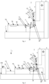
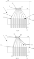
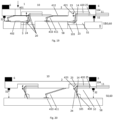
- Figure 1 illustrates an exemplary embodiment of an optical probe 1 configured for optical testing of a micro-optical component 50.
- the optical probe 1 comprises a micro-optical element 20 configured for optically coupling light 3 between the micro-optical component 50 and a testing circuit 2 at coupling locations 51, 14, wherein the light 3 is transmitted through facets 103, 102, respectively.
- the micro-optical element 20 is configured to redirect the light 3 in a 90° angle 26.
- the angle 26 may be a different angle ranging from typically 0 to 100°. Preferable values of the angle 26 may be 80° to 90°, ensuring that a total internal reflection (TIR) of the reflecting surface 23 may not fail.
- TIR total internal reflection
- the probe head 10 may be tilted 10° clockwise, as shown in Fig. 8 .
- the light 3 may travel from the testing circuit 2 to the micro-optical component 50, from the micro-optical component 50 to the testing circuit 2, or simultaneously in both directions.
- the micro-optic component 50 is fixed on a mechanical support, such as a chuck 7, either permanently or by using vacuum tools.
- an optical functionality of a functional element 56, being part of the micro-optical component 50 e.g. waveguide, laser or photodiode, which may be coupled to a waveguide 58, may be characterized, e.g. an optical transmission properties of the waveguide 58 or a spot size converter at the coupling location of the micro-optical component 50.
- a lens 24 and a planar mirror as the reflecting surface 23 are used, causing the total internal reflection.
- a planar surface and a curved mirror or a combination thereof may be used.
- the refractive index n of the micro-optical element 20 should be at least 1.53.
- the reflecting surface 23 may be a metal coated mirror, especially to avoid a failure of the total internal reflection.
- the testing circuit 2 comprises at least one waveguide 25, wherein the waveguide 25 is configured to guide light to a functional element 59, e.g. a photodetector, or a polarization sensitive splitter having two photodetectors configured for analyzing polarization.
- the functional element 59 can also be a light source.
- the testing circuit 2 may optically couple light to a fiber array ( Figure 4 ) and, preferably, modify either a mode-field diameter (compared to an optical fiber 12) or a pitch of the waveguides (compared to a fiber array 11). This embodiment may, preferably, not comprise any functional element 59.
- the testing circuit 2 is mounted here on a fixture 4 or directly on the translation stage 5.
- the part of the optical probe 1 which is movable with respect to the micro-optical component 50 is considered as the probe head 10. All components are, preferably, designed as being rather dynamic in motion, thus lightweight.
- the translation stage 5 can, preferably, be configured to control six degrees of freedom and may, preferably, be rather dynamic to allow fast testing of various micro-optical components 50.
- the testing circuit 2 may generate, receive, or generate and receive a signal configured for probing of an optical performance of the micro-optical component 50 or a part thereof, in particular of the functional element 56, the waveguide 58, or the coupling location 51.
- the optical performance may also comprise information about a quality of the facet 103, the coupling location 51 and, particularly about a spot-size converter within the waveguide 58.
- the light 3 may be used to align the probe heads 10 with respect to the micro-optical component 50.
- the testing circuit 2 may also be configured to generate a signal indicating a proximity, a distance, a collision with regard to at least one object, in particular the micro-optical component 50 or the mechanical support 7.
- the signal may, especially be generated by using a LiDAR device, a mechanical detection mechanism, an interferometric device, or a capacitive signal; however, using a different device or mechanism may also be feasible.
- the translation stage 5 is mounted to a mechanical support 6.
- the chuck 7 is a mounting device, on which the micro-optical component 50 may be temporarily or permanently fixed.
- a wafer chuck having vacuum holes, wherein the micro-optical component 50 may be part of the wafer 60 may be used.
- the chuck 7 may be translated with respect to the optical probe 1.
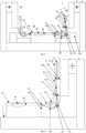
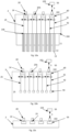
- Figure 2 illustrates a further exemplary embodiment of the optical probe 1 configured for the optical testing of the micro-optical components 50, 50b, 50c.
- the micro-optical component 50 is comprised here by a wafer 60.
- the wafer 60 may, in general, have a size of 6 inch, preferably of 8 inch, in particular of 12 inch or more, and may comprise at least 1000 micro-optical components, whereof the micro-optical components 50, 50b, 50c are, exemplarily, shown in Figure 2 .
- Measuring optical signals that may be indicative for the optical performance of the micro-optical components 50, 50b can be performed in a trench 55, which may comprise dicing lanes for wafer singulation or may have been etched for a purpose of wafer level testing. Alternatively or in addition, V-Grooves for fiber alignment etched into the wafer 60 may be used for the optical testing.
- the chuck 7 and/or the translation stage 5 may be moved to sequentially scan at least a portion of the micro-optical components 50, 50b within the wafer 60.
- Figure 3 illustrates a further exemplary embodiment of the optical probe 1 configured for the optical testing of the micro-optical component 50.
- a second probe 1b is, additionally, used here for the optical testing of a second coupling location 52 of the micro-optical component 50.
- This exemplary embodiment is configured for optically testing micro-optical component 50 having two or more coupling location 51, 52.
- the probe heads 10, 16 can be individually aligned to the micro-optical component 50.
- This exemplary embodiment can, especially, be used for micro-optical components 50 having two or more coupling location 51, 52 that may, preferably, be tested simultaneously.
- such a micro-optical component 50 may be selected from a distributed feedback (DFB) laser, where no facet is reflecting but both facets (also a rear facet) are transmitting, or an amplifier, such as s semiconductor optical amplifier (SOA) or a gain material (such as erbium) doped integrated photonic chip.
- DFB distributed feedback
- SOA semiconductor optical amplifier
- gain material such as erbium
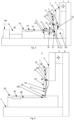
- Figure 4 illustrates a further exemplary embodiment of the optical probe 1 configured for the optical testing of the micro-optical component 50.
- the testing circuit 2 is optically coupled here to a fiber array 11 at a second coupling location 14b of the testing circuit 2.
- This exemplary embodiment may be configured for a pitch conversion from the pitch of the fiber array 11 of typically 80 ⁇ m or 127 ⁇ m or 250 ⁇ m to a pitch below 80 ⁇ m, e.g. 25 ⁇ m.
- the testing circuit 2 may, further, be configured for re-shaping a mode.
- the testing circuit 2 may be based on a platform, preferably selected from ioNext, SiN, Triplex , Si rich glass, a photonic platform as produced in a lamination process, an ion diffusion platform, a platform structured in polymer or inscribed in glass.
- This embodiment may, particularly, be favorable for testing narrow pitches of less than 80 ⁇ m.
- Figure 5 illustrates a further exemplary embodiment of the optical probe 1 configured for the optical testing of the micro-optical component 50.
- the testing circuit 2 is in mechanical contact with an electrical circuit 30.
- the testing circuit 2 may be a part of the electrical circuit 30, or the electrical circuit may be a part of the testing circuit 2, e.g. in that the testing circuit 2 may comprise at least one electrical functionality.
- This exemplary embodiment has a distance sensor 31 comprised by the electrical circuit 30, which in configured for measuring a distance 32 to the wafer 60.
- the distance sensor 31 may, alternatively or in addition, be configured of measuring a depth or a presence of the trench 55.
- the distance sensor 31 may, preferably, be selected from a capacitive sensor, an inductive sensor, or an optical sensor. In a further embodiment (not depicted here), the distance sensor 31 may be comprised by the testing circuit 2 without an electrical circuit 30, e.g. by generating a distance sensor signal to measure the distance 32 via an additional waveguide 25.
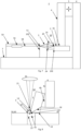
- Figure 6 illustrates a further exemplary embodiment of the optical probe 1 configured for the optical testing of the micro-optical component 50.
- the optical probe 1 is configured for optically testing of a grating coupler 105, which emits in an angle 26, which may, typically, be 95° to 115°, often 100°.
- the refractive surface 24 may be implemented in a manner that it may deflect light in a 10° angle from a surface normal to match the light emission 3 with the grating coupler 105, particularly to achieve a high optical coupling to the micro-optical component 50.
- the angle 26 can be fine-adjusted by the translation stage 5.
- the refractive surface 24 may be an optical lens emitting in a direction along the waveguide 25, while the complete probe head 10 may be tilted by an angle 26 minus 90°, typically between 0 and 20°, preferably 10°, see Figure 8 .
- Such a kind of tilting may, preferably, implemented by using a part 4b of the fixture and the micro-optical element 20, fine-adjusted by using the translation stage 5.
- Figure 7 illustrates a further exemplary embodiment of the optical probe 1 configured for the optical testing of the micro-optical component 50.
- the testing circuit 2 is or comprises a light source or a light source array, particularly selected from a laser, a laser bar, an optical amplifier (SOA), or a superluminescent light emitting diode (SLED). While the testing circuit 2 may be operated, the coupling performance may be measured by using the functional element 56, which may be an optical device, especially a photodiode.
- the optical coupling may be measured by using a further optical element, preferably an optical fiber coupled to the micro-optical component 50, the second probe head 6, a grating coupling coupled to the waveguide 58 and a camera.
- the facet 103 may, further, be equipped with an optical lens.
- the testing circuit 2 may be fixed by a vacuum gripper to the mechanical support 4 or permanently, e.g. by using an adhesive or an adhesion promoter.
- Figure 8 illustrates an exemplary embodiment of the 3D-printed marker 21.
- the marker 21 may, preferably, be produced in the same printing process as the micro-optical element 20 and may be well aligned, particularly at least to 10 ⁇ m, preferably to 5 ⁇ m, especially to 1 ⁇ m, to both the micro-optical element 20 and the coupling location 14.
- the marker 21 may be visible in a field of view of a top-view camera 33, which may for configured to provide a simplified alignment of the probe head 10 to the micro-optical component 50, especially the wafer 60, and to the trench 55.
- the mechanical fixture 4 has a part 4b which is configured to fix the testing circuit 2 at a certain angle.
- the angle may, preferably, be 5° to 15° compared to a surface normal.
- the exemplary testing circuit 2 as shown in Figure 8 comprises a chamfer 18. A region of the chamfer 18 is indicated here by a dashed line. Without the chamfer 18, a mechanical contact could occur at position assumed by the chamfer 18, which would destroy at least a portion of the micro-optical component 50, especially the wafer 60.
- the micro-optical element 20 is arranged here in a manner that the light 3 is emitted horizontally to the surface of the micro-optical component 50, especially of the wafer 60. This arrangement can be achieved by tilting the reflecting surface 23.
- Figure 9 illustrates exemplary embodiments of the testing circuit 2 connected to a fiber array 11.
- the testing circuit 2 is configured to translate a pitch 28 at the facet of the testing circuit 2 of typically 80 ⁇ m or 127 ⁇ m or 250 ⁇ m to a pitch 27 of the coupling location of the testing circuit 2 being typically below 80 ⁇ m.
- a plurality of optical fibers 12 is connected to the single micro-optical element 20.
- the pitch 27 may be 80 ⁇ m or more. This may, particularly, be favorable if
- the pitch may also be 80 ⁇ m or less.
- the waveguides 25 as well as the fiber cores 13 may be polarization maintaining. Further, the width 29a may range from 2 ⁇ m to 10 mm, preferably being 2 mm or less.
- each individual waveguide 25 is coupled to a separate channel in the micro-optical element 20, while in the exemplary embodiment of Figure 9b more than one waveguide 25e is concurrently coupled into a single channel and coupled to a single element 20e in the micro-optical element 20.
- multiplexing may be implemented by connecting several micro-optical elements 20 to a single optical fiber 12b.
- Figure 10 illustrates further exemplary embodiments of the testing circuit 2.
- a polarization splitter 40 is configured to split light of orthogonal E-vectors into two polarization channels 41, 42, which are coupled to the two optical fibers 12.
- the waveguide 25b is configured here it a manner that it does not change a polarization between a facet 102 of the testing circuit 2 and the polarization splitter 40. This advantage can, in particular, be achieved by a straight, birefringing or short waveguide.
- the micro-optical element 20 is configured here it a manner that not to change a polarization between a facet 103 of the micro-optical component 50 and the facet 102 of the testing circuit 2.
- This advantage can, in particular, be achieved by providing the micro-optical element 20 as an optical lens without reflecting surfaces or by ensuring that light may be impinging on reflecting surfaces 23 in a manner that there no alteration of phase or intensity between different polarization components may occur, which may be the case for light of which the E-field is either in the reflection plane or perpendicular to the reflection plane.
- the reflection plane is a plane defined by incoming and reflected light at a planar surface.
- the alteration of the polarization of a reflective surface may be accounted for numerically, especially by using Fresnel equation, a calibration or a training measurement.
- the complete Müller Matrix can be determined by measuring both phase and intensity of the two polarization channels 41, 42. Further, the polarization of at least a portion of light within two polarization channels 41, 42 may be rotated by 90° and interfered at a detector with each other.
- light of the two polarization channels 41, 42 is coupled to the functional element 59, which may especially be a waveguide integrated photodiode.
- the polarization of the light may be rotated by 90° or by a different angle prior to coupling into a fiber or a functional element 59, especially a photodetector.
- the functional elements 59 are configured for testing properties of the micro-optical component 50 either by transmitting or receiving or by receiving and transmitting light at the same time.
- the functional elements 59 may be selected from at least one of a photodiode, especially PIN, PN, or APD; a waveguide integrated photodiode; an IQ-receiver; a beam combiner; an optical modulator; a light source, especially a laser or an SLED; an amplifier, especially an SOA; an IQ modulator; an intensity modulator; a polarization splitter; a polarization stripper; a polarization filter, especially a rating coupler; or a polarization rotator.
- the waveguides 25 may be single-mode or multimode. Further, the waveguides 25 may be arranged at an angle ⁇ 0° to the facet 102 of the testing circuit 2, in particular to reduce reflections. Further, the micro-optical element 20 may have only angled surfaces with respect to the light propagation, in particular to avoid back-reflections, see Figure 11 .
- the functional elements 59 in particular the IQ receiver or the beam combiner, may be used to measure the phase of two light beams relative to each other and may be used as feedback signal to trim the waveguide 58.
- Figure 11 illustrates a further exemplary embodiment of the optical probe 1 configured for the optical testing of the micro-optical component 50.
- the waveguides 25c, 58b are configured not to be normal to the surfaces of the facets 102, 103, respectively.
- the refractive surface 24 of the micro-optical element 20 deflects the light 3 in a manner that it may couple well between the waveguides 25c, 58b.
- the refractive surface 24 of the micro-optical element 20 may have no optically effective surfaces which are perpendicular to the beam propagation direction of the light 3. This embodiment may be favorable, particularly since it may suppress back-reflection due to the angled surfaces.
- the reflecting surface 23 may also have no surfaces perpendicular to the propagation direction of the light 3.
- an optical isolator and/or an additional anti-reflective coating may be used on at least one of the facets 102, 103 or on the refractive surface 24 of the micro-optical element 20.
- Figure 12 illustrates a further exemplary embodiment of the optical probe 1 configured for the optical testing of the micro-optical components 50, 50b, 50c.
- the testing circuit 2 has a large number of coupling locations 14.
- several or all coupling locations 14 are equipped with one or more micro-optical elements 20.
- Each coupling location 14 may be selected from a grating coupler, a photodetector, an adiabatic taper, an etched facet, an etched facet in an angle of 30 to 120° with respect to the surface normal of the facet 102, or a VCSEL array.
- the micro-optical element 20 may be or comprise a refractive surface 24 that may be shaped in a manner as schematically shown in Figure 6 that the light 3 being perpendicular to the facet 102 may be received to a large extent.
- the probe head 10 may be designed to have a minimum or a maximum alteration of sensitivity with respect to the amount of the light 3 coupled into the coupling location 14 by either using a high-NA lens or a low-NA lens as the refractive surface 24, wherein NA denotes a "numerical aperture". This embodiment can be used for measuring a spatial and/or angular distribution of the light 3.
- the light 3 may be either come from the micro-optical component 50, then the coupling location 14 may receive the light 3, or the light 3 may be transmitted into the micro-optical component 50, then the coupling location 14 may emit the light 3.
- the probe head 10 may function as a Shack-Hartmann sensor, in particular by measuring at least one of a propagation direction or an intensity of the light 3. During a measurement, the probe head 10 may be moved according to a programmed pattern for sub-sampling, in particular by measuring the light 3 at more locations than micro-optical element 20 are present. In a preferred embodiment, at least a region 19 may be removed, especially by thinning, etching, or milling, for fitting the probe head 10 into smaller trenches 55.
- a thin testing circuit 2 having a thickness 19b, preferably of 730 ⁇ m or less, more preferred of 100 ⁇ m or less, over the complete component or at least in the region 19.
- a thin substrate especially prepared by using a direct bandgap semiconductor, may be used.
- FIG 13 illustrates a facet view directed at the facet 102 of a testing circuit 2.
- each micro-optical element 20 has a preferable diameter 110a.
- each micro-optical element 20 has a diameter 110b, wherein adjacent micro-optical elements 20 are intersecting.
- each micro-optical element 20 has a diameter 110b, wherein adjacent micro-optical elements 20 are separated by leaving a gap 111.
- the gap 111 may be advantageous for mechanically decoupling the adjacent micro-optical elements 20 which is preferable for a higher reliability of the probe head 10.
- Figure 14a illustrates the further exemplary embodiment of the optical probe 1 in a projection direction along +z according to Figure 2 . Dashed lines indicate part of elements of the drawing that are not visible since they are covered by another element.
- the micro-optical component 50 comprises waveguides 58, each having a pitch 28b.
- the pitch 28b may be 30 ⁇ m or less. Providing a probe having a pitch 27 that may match pitch 28b would, however, lead to rather small micro-optical element 20, leading to a short working distance 34 or to poor coupling between the coupling locations 14, 51 due to the rather too small micro-optical elements 20.
- a plurality of coupling locations 14 couple with, preferably, at least one waveguide 58c at a coupling location 51b in the embodiment of Figure 14a .
- This arrangement can be achieved by interfering light originating from the plurality of coupling locations 14, wherein the light has a phase that is adjusted in a manner that the light constructively interferes at the coupling location 51b such that the mode-field generated at the coupling location 51b, preferably, corresponds to the mode field that couples best into the coupling location 51b.
- the mode-field coupling best into the coupling location 51b is the mode-field that corresponds to the coupling location 51b as much as possible in intensity distribution and phase distribution.
- the phase and amplitude of the light emitted by the coupling locations 14 is adjusted in a manner that a concentric wave-front is generated in the center of the coupling location 51b. Additionally, the coupling sites 14 that are further away from the coupling location 51b may be reduced in intensity to generate an appropriate mode-field size.
- This principle as used in the embodiment of Figure 14a can be referred to as "optical phase array”.
- the appropriate phase may be adjusted by cascade phase shifters within the testing circuit 2.
- the phase shifters may be operated by changing the refractive index controlling the phase and/or intensity of the light, especially by using at least one of heat, a current injection into a semiconductor junction, a piezo electric element, a voltage applied to a material that changes its refractive index upon an electric field, or a silicon-organic hybrid modulator.
- the optical phase array is configured for addressing the plurality of the coupling locations 51b without mechanical movement.
- the micro-optical elements 20 may be further configured for enabling light propagating, preferably from every coupling location 14 to every coupling location 51. This can, particularly, be achieved by designing individual micro-optical elements 20 having a high NA in the drawing plane of Figure 14a .
- the optical probe 1 by using the exemplary embodiment of the optical probe 1 according to Figure 14a it is possible to probe a large number of coupling locations 14, in particular more than 100, having a small pitch, especially of 30 ⁇ m or less, in a fast time, preferably within 100 ms or less per connection, by using a large working distance, especially of 30 ⁇ m or more, under adjustment of the incident angle in the drawing plane of Figure 14a .
- a plurality of mode-fields may be generated, in particular for allowing to probe components having a highly irregular pitch 28b or for using a single probe head 10 for probing various different micro-optical components 50.
- Figure 14b illustrates the further exemplary embodiment of the optical probe 1 in an observation projection direction along +x according to Figure 14 .
- each refractive surface 24 of the coupling locations 14 are elongated along the waveguide 25 in a manner that the light can be well-focused in the out-of-plane direction of Figure 14b .
- the each coupling location 14 is as high as a distance of the simultaneously emitting elements in Figure 14 , or such that each refractive surface 24 is at least capturing 50 %, preferably 90 % of an emission of the light distribution emitted by the coupling location 51 in an out-of-plane direction according to Figure 14b .
- Figure 15 illustrates a further exemplary embodiment of the optical probe 1 configured for the optical testing of the micro-optical components 50, 50b, 50c.
- the testing circuit 2 has a position sensitive device 14c.
- the position sensitive device 14c can detect the tilt angle of a facet 103b, dashed line, and can distinguish the tilt angle of the facet 103b from a straight facet 103. This procedures can identify facets that are not perpendicular, which is a common fabrication deviation.
- the optical probe 1 is configured to detect the tilted facet 103b by detecting light propagating along a center ray 3d.
- the position sensitive device 14c may, preferably, be located in or close to a Fourier plane of the center ray 3d, which causes the center of the light distribution to be displaced on the position sensitive device 14c depending on an orientation of the tilted facet 103b.
- the position sensitive device 14c may be located in the image plane for imaging the coupling location 51.
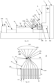
- Figure 16 illustrates a method for producing the probe head 10.
- An objective lens 201 generates a laser beam 202 configured for curing a photoresist 200.
- the solubility of the photoresist 200 may be changed by the irradiation of the laser beam 202.
- the structures 20b constituting a micro-optical element are produced.
- light 15 may be coupled into the testing circuit 2.
- the light 15 is chosen in a manner that it may be transmitted by the waveguides 25.
- the lithography system 210 has a detector configured to detect the position of light 15 exciting the testing circuit 2 through coupling locations 14.
- the detector may be a CCD camera, or a confocal detector.
- the laser beam 202 may be coupled to the probe head 10 through the coupling locations 14 and is detected at the fiber core 13 or by a detector within the testing circuit 2 coupled to the probe head 10.
- a feature within the testing circuit 2 especially the waveguide 25 or the marker 21 (not depicted here), may be used for the alignment.
- light of the laser beam 202 coupling into the waveguides 25 and being reflected at a feature within waveguide 25, such as the facet 104 or at the fiber core 13, may be detected.
- Figure 17 illustrates a further exemplary embodiment of the optical probe 1 configured for the optical testing of the micro-optical component 50.
- the micro-optical element 20 has a mechanical support 8 configured for providing a certain distance, especially 5 ⁇ m to 250 ⁇ m, between the refractive surface 24 and the facet 102.
- the micro-optical element 20 may also be attached to the fixture 4 for the testing circuit 2, in this case, the fixture 4 may, preferably, be arranged in a manner that it is not flush with the facet 102 but protrudes from the facet 102.
- the refractive surface 24b here implemented as an optical lens, can reduce a divergence of then light 3 to avoid failure of total internal reflection at the region 9. Additionally, the angle 26 may exceed 90° to mitigate failure of the total internal reflection.
- the testing circuit 2 may have at least one optical 3D-printed element, preferably an on-chip mode-field converter, configured to reduce the divergence of the light 3, which is fabricated close to facet 102. This embodiment according to Figure 17 may be favorable, if the divergent light 3e emitted or collected by the pitch at the facet 103b may be more divergent than light emitted by a standard single mode fiber, such as the single mode fiber 28.
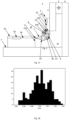
- Figure 18 illustrates experimental results obtained in a mode-field diameter statistics of 250 micro-optical elements 20, which were implemented as optical lenses.
- a mode-field diameter w is normalized to a design mode field w 0 .
- a standard deviation of 2 % could be achieved.
- Figure 19 illustrates a further exemplary embodiment, in which the probe head 10 comprises a probe-card made out of a printed circuit board (PCB), a wafer, or a planar light wave circuit (PLC) comprising both electrical cantilevers 411 and electrical transmission line 412 as well as a micro-electrical mechanical system (MEMS) actuator 420 having an optical waveguide.
- a hole or a via 401 may allow aligning the probe head 10 to the micro-optical component 50 by observing a fiducial 402.
- the electrical cantilever 411 can, in an initial contact step, be aligned with the electrical contact pad 410 of the wafer 60.
- the micro-optical element 20 can be aligned by using the MEMS actuator 420 to couple the light 3.
- the MEMS actuator 420 can move the micro-optical element 20 by at least 1 ⁇ m, preferably by at least 10 ⁇ m, especially by at least 25 ⁇ m or more.
- a plurality of cantilevers 411 and a plurality of micro-optical elements 20, in some embodiments at least 1000, may be present.
- the PLC may further comprise optical switches, optical splitters, or optical detectors.
- the PLC may be connected to the optical probe 1 either electrically or by using the fiber array 11.
- the optical probe 1 may, additionally, comprise the distance sensor 31, which is configured to measure the distance 32 between the distance sensor 31 and a surface of the wafer 60.
- the distance sensor 31 may, preferably be selected from at least one of an optical sensor or a capacitive sensor.
- Figure 20 illustrates a further exemplary embodiment, in which the probe head 10 is configured to test a functionality of a beam-shaping element 430, in particular an emission direction.
- the MEMS actuator 420 may be configured to provide at least one of a rotation or a translation of the micro-optical element 20.
- the micro-optical element 20 is configured to redirect the light 3 to an angle that allows coupling it into the grating coupler 105.
- the reflecting surface 23 is also configured to redirect the light from the waveguide 25 towards the surface of the wafer 60.
Landscapes
- Physics & Mathematics (AREA)
- General Physics & Mathematics (AREA)
- Chemical & Material Sciences (AREA)
- Analytical Chemistry (AREA)
- Optics & Photonics (AREA)
- Optical Couplings Of Light Guides (AREA)
- Testing Of Optical Devices Or Fibers (AREA)
- Semiconductor Lasers (AREA)
Applications Claiming Priority (1)
| Application Number | Priority Date | Filing Date | Title |
|---|---|---|---|
| EP23218488.7A EP4575444A1 (de) | 2023-12-20 | 2023-12-20 | Optische sonde und zugehörige verfahren |
Publications (1)
| Publication Number | Publication Date |
|---|---|
| EP4575445A1 true EP4575445A1 (de) | 2025-06-25 |
Family
ID=89430323
Family Applications (2)
| Application Number | Title | Priority Date | Filing Date |
|---|---|---|---|
| EP23218488.7A Pending EP4575444A1 (de) | 2023-12-20 | 2023-12-20 | Optische sonde und zugehörige verfahren |
| EP24221372.6A Pending EP4575445A1 (de) | 2023-12-20 | 2024-12-19 | Optische sonde und zugehörige verfahren |
Family Applications Before (1)
| Application Number | Title | Priority Date | Filing Date |
|---|---|---|---|
| EP23218488.7A Pending EP4575444A1 (de) | 2023-12-20 | 2023-12-20 | Optische sonde und zugehörige verfahren |
Country Status (4)
| Country | Link |
|---|---|
| US (1) | US20250207995A1 (de) |
| EP (2) | EP4575444A1 (de) |
| CN (1) | CN120176993A (de) |
| TW (1) | TW202526402A (de) |
Families Citing this family (1)
| Publication number | Priority date | Publication date | Assignee | Title |
|---|---|---|---|---|
| CN120629900A (zh) * | 2025-08-06 | 2025-09-12 | 苏州联讯仪器股份有限公司 | 一种硅光晶圆测试方法及一种硅光晶圆测试装置 |
Citations (5)
| Publication number | Priority date | Publication date | Assignee | Title |
|---|---|---|---|---|
| WO2018083191A1 (de) | 2016-11-02 | 2018-05-11 | Karlsruher Institut für Technologie | Verfahren zur herstellung eines optischen systems und optisches system |
| US20180143245A1 (en) | 2016-11-21 | 2018-05-24 | Si-Ware Systems | Integrated optical probe card and system for batch testing of optical mems structures with in-plane optical axis using micro-optical bench components |
| EP4001980A1 (de) | 2020-11-24 | 2022-05-25 | Intel Corporation | Kontaktloses optisches abtasten einer kantengekoppelten photonischen ic |
| WO2022266760A1 (en) | 2021-06-23 | 2022-12-29 | Universite Laval | Printed photonic component based photonic device probing and testing |
| WO2023132785A1 (en) | 2022-01-06 | 2023-07-13 | Compoundtek Pte. Ltd. | Apparatus for wafer level testing of semicondcutor device |
-
2023
- 2023-12-20 EP EP23218488.7A patent/EP4575444A1/de active Pending
-
2024
- 2024-12-19 TW TW113149608A patent/TW202526402A/zh unknown
- 2024-12-19 CN CN202411882137.4A patent/CN120176993A/zh active Pending
- 2024-12-19 US US18/986,905 patent/US20250207995A1/en active Pending
- 2024-12-19 EP EP24221372.6A patent/EP4575445A1/de active Pending
Patent Citations (6)
| Publication number | Priority date | Publication date | Assignee | Title |
|---|---|---|---|---|
| WO2018083191A1 (de) | 2016-11-02 | 2018-05-11 | Karlsruher Institut für Technologie | Verfahren zur herstellung eines optischen systems und optisches system |
| US20190258175A1 (en) * | 2016-11-02 | 2019-08-22 | Karlsruhe Institute Of Technology | Method for producing an optical system and optical system |
| US20180143245A1 (en) | 2016-11-21 | 2018-05-24 | Si-Ware Systems | Integrated optical probe card and system for batch testing of optical mems structures with in-plane optical axis using micro-optical bench components |
| EP4001980A1 (de) | 2020-11-24 | 2022-05-25 | Intel Corporation | Kontaktloses optisches abtasten einer kantengekoppelten photonischen ic |
| WO2022266760A1 (en) | 2021-06-23 | 2022-12-29 | Universite Laval | Printed photonic component based photonic device probing and testing |
| WO2023132785A1 (en) | 2022-01-06 | 2023-07-13 | Compoundtek Pte. Ltd. | Apparatus for wafer level testing of semicondcutor device |
Non-Patent Citations (4)
| Title |
|---|
| SINGER S. ET AL.: "3D-printed facet-attached optical elements for beam shaping in optical phased arrays", OPT. EXPRESS, vol. 30, 2022, pages 46564 - 46574 |
| STEFAN SINGER ET AL.: "3D-printed facet-attached optical elements for beam shaping in optical phased arrays", 24 March 2022, CORNELL UNIVERSITY LIBRARY |
| STEFAN SINGER ET AL: "3D-printed facet-attached optical elements for beam shaping in optical phased arrays", ARXIV.ORG, CORNELL UNIVERSITY LIBRARY, 201 OLIN LIBRARY CORNELL UNIVERSITY ITHACA, NY 14853, 24 March 2022 (2022-03-24), XP091183926 * |
| TRAPPEN M. ET AL.: "3D-printed optical probes for wafer-level testing of photonic integrated circuits", OPTICS EXPRESS, vol. 28, 2020, pages 37996 - 38007 |
Also Published As
| Publication number | Publication date |
|---|---|
| TW202526402A (zh) | 2025-07-01 |
| US20250207995A1 (en) | 2025-06-26 |
| CN120176993A (zh) | 2025-06-20 |
| EP4575444A1 (de) | 2025-06-25 |
Similar Documents
| Publication | Publication Date | Title |
|---|---|---|
| US11946950B2 (en) | Electro-optical circuit board for contacting photonic integrated circuits | |
| JP7430756B2 (ja) | 光学システムを製造する方法および光学システム | |
| US11480495B2 (en) | Position-tolerance-insensitive contacting module for contacting optoelectronic chips | |
| US20200241220A1 (en) | Optical assemblies, interconnection substrates and methods for forming optical links in interconnection substrates | |
| US7378861B1 (en) | Optical alignment loops for the wafer-level testing of optical and optoelectronic chips | |
| US7184626B1 (en) | Wafer-level testing of optical and optoelectronic chips | |
| US20070148792A1 (en) | Wafer measurement system and apparatus | |
| CN110140038B (zh) | 用于使用微光学平台组件对具有面内光轴的光学mems结构进行批量测试的集成光学探针卡和系统 | |
| WO2018022318A1 (en) | Optical assemblies, interconnection substrates and methods for forming optical links in interconnection substrates | |
| JP7588651B2 (ja) | 光結合点の位置特定 | |
| WO2020123164A1 (en) | Image distance in lidar systems | |
| EP4575445A1 (de) | Optische sonde und zugehörige verfahren | |
| CN119269504A (zh) | 用于晶圆检测的调焦装置、调焦方法、系统和计算机存储介质 | |
| KR20150048971A (ko) | 광섬유를 이용한 미세 패턴의 선폭 및 깊이 측정 장치 및 측정 방법 | |
| EP4621457A1 (de) | Optische sonde und zugehörige verfahren | |
| EP4575446A1 (de) | Positionierung eines optischen wellenleiters an einer photonischen integrierten schaltung | |
| WO2003044504A2 (en) | Optical probe for wafer scale testing of light-electrical (l-i-v) performance of optoelectronic devices | |
| KELDER | ON WAFER LEVEL |
Legal Events
| Date | Code | Title | Description |
|---|---|---|---|
| PUAI | Public reference made under article 153(3) epc to a published international application that has entered the european phase |
Free format text: ORIGINAL CODE: 0009012 |
|
| STAA | Information on the status of an ep patent application or granted ep patent |
Free format text: STATUS: THE APPLICATION HAS BEEN PUBLISHED |
|
| AK | Designated contracting states |
Kind code of ref document: A1 Designated state(s): AL AT BE BG CH CY CZ DE DK EE ES FI FR GB GR HR HU IE IS IT LI LT LU LV MC ME MK MT NL NO PL PT RO RS SE SI SK SM TR |
|
| STAA | Information on the status of an ep patent application or granted ep patent |
Free format text: STATUS: REQUEST FOR EXAMINATION WAS MADE |
|
| 17P | Request for examination filed |
Effective date: 20251218 |