EP4572538A1 - Adhesive base material with wiring line, multilayer device, glass laminate, and method for producing adhesive base material with wiring line - Google Patents
Adhesive base material with wiring line, multilayer device, glass laminate, and method for producing adhesive base material with wiring line Download PDFInfo
- Publication number
- EP4572538A1 EP4572538A1 EP23852230.4A EP23852230A EP4572538A1 EP 4572538 A1 EP4572538 A1 EP 4572538A1 EP 23852230 A EP23852230 A EP 23852230A EP 4572538 A1 EP4572538 A1 EP 4572538A1
- Authority
- EP
- European Patent Office
- Prior art keywords
- adhesive layer
- wiring
- substrate
- adhesive
- layer
- Prior art date
- Legal status (The legal status is an assumption and is not a legal conclusion. Google has not performed a legal analysis and makes no representation as to the accuracy of the status listed.)
- Pending
Links
Images


Classifications
-
- H—ELECTRICITY
- H05—ELECTRIC TECHNIQUES NOT OTHERWISE PROVIDED FOR
- H05K—PRINTED CIRCUITS; CASINGS OR CONSTRUCTIONAL DETAILS OF ELECTRIC APPARATUS; MANUFACTURE OF ASSEMBLAGES OF ELECTRICAL COMPONENTS
- H05K1/00—Printed circuits
- H05K1/02—Details
- H05K1/0271—Arrangements for reducing stress or warp in rigid printed circuit boards, e.g. caused by loads, vibrations or differences in thermal expansion
-
- B—PERFORMING OPERATIONS; TRANSPORTING
- B32—LAYERED PRODUCTS
- B32B—LAYERED PRODUCTS, i.e. PRODUCTS BUILT-UP OF STRATA OF FLAT OR NON-FLAT, e.g. CELLULAR OR HONEYCOMB, FORM
- B32B17/00—Layered products essentially comprising sheet glass, or glass, slag, or like fibres
-
- B—PERFORMING OPERATIONS; TRANSPORTING
- B32—LAYERED PRODUCTS
- B32B—LAYERED PRODUCTS, i.e. PRODUCTS BUILT-UP OF STRATA OF FLAT OR NON-FLAT, e.g. CELLULAR OR HONEYCOMB, FORM
- B32B7/00—Layered products characterised by the relation between layers; Layered products characterised by the relative orientation of features between layers, or by the relative values of a measurable parameter between layers, i.e. products comprising layers having different physical, chemical or physicochemical properties; Layered products characterised by the interconnection of layers
- B32B7/02—Physical, chemical or physicochemical properties
- B32B7/025—Electric or magnetic properties
-
- H—ELECTRICITY
- H01—ELECTRIC ELEMENTS
- H01B—CABLES; CONDUCTORS; INSULATORS; SELECTION OF MATERIALS FOR THEIR CONDUCTIVE, INSULATING OR DIELECTRIC PROPERTIES
- H01B13/00—Apparatus or processes specially adapted for manufacturing conductors or cables
-
- H—ELECTRICITY
- H01—ELECTRIC ELEMENTS
- H01B—CABLES; CONDUCTORS; INSULATORS; SELECTION OF MATERIALS FOR THEIR CONDUCTIVE, INSULATING OR DIELECTRIC PROPERTIES
- H01B5/00—Non-insulated conductors or conductive bodies characterised by their form
- H01B5/14—Non-insulated conductors or conductive bodies characterised by their form comprising conductive layers or films on insulating-supports
-
- H—ELECTRICITY
- H05—ELECTRIC TECHNIQUES NOT OTHERWISE PROVIDED FOR
- H05K—PRINTED CIRCUITS; CASINGS OR CONSTRUCTIONAL DETAILS OF ELECTRIC APPARATUS; MANUFACTURE OF ASSEMBLAGES OF ELECTRICAL COMPONENTS
- H05K1/00—Printed circuits
- H05K1/02—Details
- H05K1/03—Use of materials for the substrate
-
- H—ELECTRICITY
- H05—ELECTRIC TECHNIQUES NOT OTHERWISE PROVIDED FOR
- H05K—PRINTED CIRCUITS; CASINGS OR CONSTRUCTIONAL DETAILS OF ELECTRIC APPARATUS; MANUFACTURE OF ASSEMBLAGES OF ELECTRICAL COMPONENTS
- H05K1/00—Printed circuits
- H05K1/02—Details
- H05K1/03—Use of materials for the substrate
- H05K1/0306—Inorganic insulating substrates, e.g. ceramic, glass
-
- H—ELECTRICITY
- H05—ELECTRIC TECHNIQUES NOT OTHERWISE PROVIDED FOR
- H05K—PRINTED CIRCUITS; CASINGS OR CONSTRUCTIONAL DETAILS OF ELECTRIC APPARATUS; MANUFACTURE OF ASSEMBLAGES OF ELECTRICAL COMPONENTS
- H05K1/00—Printed circuits
- H05K1/02—Details
- H05K1/09—Use of materials for the conductive, e.g. metallic pattern
- H05K1/092—Dispersed materials, e.g. conductive pastes or inks
-
- H—ELECTRICITY
- H05—ELECTRIC TECHNIQUES NOT OTHERWISE PROVIDED FOR
- H05K—PRINTED CIRCUITS; CASINGS OR CONSTRUCTIONAL DETAILS OF ELECTRIC APPARATUS; MANUFACTURE OF ASSEMBLAGES OF ELECTRICAL COMPONENTS
- H05K3/00—Apparatus or processes for manufacturing printed circuits
- H05K3/38—Improvement of the adhesion between the insulating substrate and the metal
-
- H—ELECTRICITY
- H05—ELECTRIC TECHNIQUES NOT OTHERWISE PROVIDED FOR
- H05K—PRINTED CIRCUITS; CASINGS OR CONSTRUCTIONAL DETAILS OF ELECTRIC APPARATUS; MANUFACTURE OF ASSEMBLAGES OF ELECTRICAL COMPONENTS
- H05K3/00—Apparatus or processes for manufacturing printed circuits
- H05K3/46—Manufacturing multilayer circuits
- H05K3/4644—Manufacturing multilayer circuits by building the multilayer layer by layer, i.e. build-up multilayer circuits
- H05K3/4664—Adding a circuit layer by thick film methods, e.g. printing techniques or by other techniques for making conductive patterns by using pastes, inks or powders
-
- C—CHEMISTRY; METALLURGY
- C09—DYES; PAINTS; POLISHES; NATURAL RESINS; ADHESIVES; COMPOSITIONS NOT OTHERWISE PROVIDED FOR; APPLICATIONS OF MATERIALS NOT OTHERWISE PROVIDED FOR
- C09J—ADHESIVES; NON-MECHANICAL ASPECTS OF ADHESIVE PROCESSES IN GENERAL; ADHESIVE PROCESSES NOT PROVIDED FOR ELSEWHERE; USE OF MATERIALS AS ADHESIVES
- C09J9/00—Adhesives characterised by their physical nature or the effects produced, e.g. glue sticks
-
- H—ELECTRICITY
- H05—ELECTRIC TECHNIQUES NOT OTHERWISE PROVIDED FOR
- H05K—PRINTED CIRCUITS; CASINGS OR CONSTRUCTIONAL DETAILS OF ELECTRIC APPARATUS; MANUFACTURE OF ASSEMBLAGES OF ELECTRICAL COMPONENTS
- H05K2201/00—Indexing scheme relating to printed circuits covered by H05K1/00
- H05K2201/10—Details of components or other objects attached to or integrated in a printed circuit board
- H05K2201/10431—Details of mounted components
- H05K2201/10507—Involving several components
- H05K2201/10522—Adjacent components
-
- H—ELECTRICITY
- H05—ELECTRIC TECHNIQUES NOT OTHERWISE PROVIDED FOR
- H05K—PRINTED CIRCUITS; CASINGS OR CONSTRUCTIONAL DETAILS OF ELECTRIC APPARATUS; MANUFACTURE OF ASSEMBLAGES OF ELECTRICAL COMPONENTS
- H05K2203/00—Indexing scheme relating to apparatus or processes for manufacturing printed circuits covered by H05K3/00
- H05K2203/07—Treatments involving liquids, e.g. plating, rinsing
- H05K2203/0779—Treatments involving liquids, e.g. plating, rinsing characterised by the specific liquids involved
- H05K2203/0783—Using solvent, e.g. for cleaning; Regulating solvent content of pastes or coatings for adjusting the viscosity
Definitions
- the present disclosure relates to wiring-attached adhesive substrate, stacked device, glass stacked body, and a method for manufacturing wiring attached adhesive substrate.
- Tiling technology is one of the technologies for forming large size electronic devices.
- Tiling technology is a technology in which a plurality of electronic devices is arrayed on a substrate and adjacent electronic devices are electrically connected to form a large size electronic device.
- plural display devices are arrayed on a substrate and these display devices can be electrically connected to form a large screen display device.
- Patent Document 1 discloses a transfer film for forming a transparent conductive layer and a technique for manufacturing a transparent conductive laminate using the transfer film.
- Patent Literature 1 Japanese Patent No. 5430792
- the inventor of the present application has considered a technique for directly forming a wiring pattern on an adhesive layer.
- a new problem was found that crack and buckling occur in the formed wiring.
- an object of the present disclosure is to provide a wiring-attached adhesive substrate, a stacked device, and glass stacked body that can suppress the occurrence of crack and buckling in the wiring pattern formed on the adhesive layer, as well as to provide a method for manufacturing the wiring attached adhesive substrate.
- the wiring-attached adhesive substrate includes a substrate, an adhesive layer formed on the substrate, and a wiring pattern formed on the adhesive layer.
- the adhesive layer has an adhesive strength of 0.01 N/25 mm or more to a PET film, a layer thickness variation when the adhesive layer is immersed in isopropyl alcohol for 1 minute is 20% or less, and a layer thickness variation when the adhesive layer is immersed in toluene for 1 minute is 18% or less.
- the wiring pattern may be composed of a material containing at least one selected from the group consisting of silver, copper, carbon, and gold.
- a light transmittance of the entire surface of the wiring-attached adhesive substrate may be 50% or more.
- a stacked device includes a wiring-attached adhesive substrate described above and an electronic device disposed on the wiring-attached adhesive substrate.
- the electronic device is electrically connected to the wiring pattern formed on the adhesive layer.
- the stacked device described above may further includes an over coat layer covering the electronic device and the wiring pattern.
- a glass stacked body according to one aspect of the present disclosure is a glass stacked body in which the stacked device described above is encapsulated in a glass plate or laminated to the surface of a glass plate.
- a method for manufacturing a wiring-attached adhesive substrate includes a step of forming an adhesive layer on a substrate and a step of forming a wiring pattern on the adhesive layer using a conductive ink material.
- the adhesive layer uses a material having an adhesive strength of 0.01 N/25 mm or more to a PET film, a layer thickness variation of 20% or less when the adhesive layer is immersed in isopropyl alcohol for 1 minute, and a layer thickness variation of 18% or less when the adhesive layer is immersed in toluene for 1 minute.
- the step of forming a wiring pattern may be a step of printing the conductive ink material on the adhesive layer using inkjet technique to form the wiring pattern.
- the step of forming a wiring pattern may be a step of printing the conductive ink material on the adhesive layer using screen printing technique to form the wiring pattern.
- the present disclosure can provide a wiring-attached adhesive substrate, a stacked device, and glass stacked body that can suppress the occurrence of crack and buckling in the wiring pattern formed on the adhesive layer, as well as to provide a method for manufacturing the wiring-attached adhesive substrate.
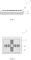
- Fig. 1 is a cross-sectional view showing a configuration example of a wiring-attached adhesive substrate according to the embodiment.
- the wiring-attached adhesive substrate 1 according to the present embodiment includes a substrate 10, adhesive layer 11, and wiring pattern 12.
- the wiring pattern 12 may be simply described as wiring 12.
- the substrate 10 is a component for supporting a plurality of electronic devices 15 (see Fig. 2 ) adhered using the adhesive layer 11.
- the substrate 10 may be configured with a rigid material or a flexible material.
- the substrate 10 may be configured using a transparent material, or may be configured using a material having a small retardation value to prevent rainbow unevenness during observation.
- TAC Triacetylcellulose
- acrylic resin acrylic resin
- COP Cyclo Olefin Polymer
- CPI Colorless and Transparent Polyimide
- the thickness of the substrate 10 is, for example, about 12 ⁇ m to 250 ⁇ m.
- the thickness of the substrate 10 may be changed according to the processability of a post-process such as laminated glass encapsulation.
- a functional layer may be provided separately on the substrate 10.
- the functional layer is an easy-to-adhere layer, an oxygen barrier layer, a water vapor barrier layer, an invisible layer, an antistatic layer and the like.
- the adhesive layer 11 is formed on the substrate 10, and is a component for adhering a plurality of electronic devices 15 (see Fig. 2 ) to the substrate 10.
- a transparent adhesive material that is, an Optical Clear Adhesive (OCA)
- OCA Optical Clear Adhesive
- the thickness of the adhesive layer 11 is, for example, 5 ⁇ m to 200 ⁇ m. Details of the adhesive layer 11 will be described later.
- the wiring pattern 12 is formed on the adhesive layer 11.
- the wiring pattern 12 can be formed by drawing directly on the adhesive layer 11.
- the wiring pattern 12 can be formed by printing a conductive ink material on the adhesive layer 11 using inkjet technique.
- the wiring pattern 12 may be formed by printing the conductive ink material on the adhesive layer 11 using screen printing technique.
- the wiring pattern 12 can be composed of a material containing at least one selected from the group consisting of silver, copper, carbon, and gold. That is, the wiring pattern 12 may be formed using the conductive ink material (wiring ink material) containing at least one selected from the group consisting of silver, copper, carbon, and gold.
- the wiring width of the wiring pattern 12 is, for example, 1.5 ⁇ m to 10 mm.
- the wiring-attached adhesive substrate 1 according to the present embodiment may be transparent.
- the light transmittance of the entire surface of the wiring-attached adhesive substrate according to the present embodiment may be 50% or more, preferably 60% or more, and more preferably 80% or more.
- the light transmittance of the entire surface of the wiring-attached adhesive substrate is the average value of the total light transmittance of entire area of the substrate regardless of the installation location of the wiring.
- Fig. 2 is a plan view illustrating a configuration example of the stacked device 2 according to the embodiment.
- Fig. 3 is a cross-sectional view illustrating a configuration example of the stacked device 2 according to the embodiment.
- the plurality of electronic devices 15 is disposed on the wiring-attached adhesive substrate 1. Specifically, the plurality of electronic devices 15 is adhered to the adhesive layer 11 of the wiring-attached adhesive substrate 1. As a result, the plurality of electronic devices 15 is fixed to the substrate 10. At this time the electronic device 15 is electrically connected to the wiring pattern 12 formed on the adhesive layer 11.
- the electronic device 15 is a display device, an optical device, a sensor device, a heating device, and the like, and a connecting component such as Flexible Printed Circuits (FPC) may also be connected.
- the electronic device 15 may be an electronic device besides these.
- the stacked device according to the present embodiment may include an over coat layer 16 and a substrate 17 as shown in the stacked device 3 shown in Fig. 4 .
- the over coat layer 16 is a component that covers and protects a plurality of electronic devices 15 and wiring pattern 12. Specifically, by providing the over coat layer 16, chemical degradation such as oxidation and corrosion of the electronic device 15 and the wiring pattern 12 can be suppressed. Furthermore, when the over coat layer 16 is provided, local pressure is applied to the edge portion or the like where the wiring-attached adhesive substrate 1 and the electronic device 15 come into contact, and mechanical degradation such as wire breakage can suppressed.
- a curing resin, Optical Clear Resin (OCR), and the like can be used for example.
- the substrate 17 is a component protecting the plurality of electronic devices 15, and can be effectively protected by sandwiching the plurality of electronic devices 15 between the lower side substrate 10 and the upper side substrate 17.
- the same material of as the substrate 10 described above can be used for the substrate 17.
- the over coat layer 16 includes adhesiveness, and the substrate 17 can be adhered to the over coat layer 16 by arranging the substrate 17 on the over coat layer 16.
- the substrate 17 may be separately provided with a functional layer in the same manner as the substrate 10.
- the functional layer is an easy-to-adhere layer, an oxygen barrier layer, a water vapor barrier layer, an invisible layer, an antistatic layer and the like.
- the stacked device 3 shown in Fig. 4 may be configured to be encapsulated in a glass plate or laminated to a glass plate surface to form a glass stacked body.
- Fig. 5 is a cross-sectional view showing configuration example of a glass stacked body according to the embodiment.
- Fig. 5 shows an example in which the laminating device 3 shown in Fig. 4 is encapsulated in a glass plate to form glass stacked body 4.
- the glass stacked body 4 shown in Fig. 5 includes intermediate bonding layers 21a, 21b on the upper surface and the lower surface of the stacked device 3, respectively.
- intermediate bonding layers 21a, 21b for example, polyvinyl butyral (PVB), ethylene-vinyl acetate copolymer (EVA), and the like can be used.
- Glass plates 22a and 22b are provided on the outer surfaces of each intermediate bonding layers 21a and 21b.
- inorganic glass can be used.
- the inorganic glass include soda-lime glass, aluminosilicate glass, borosilicate glass, alkali-free glass, and quartz glass.
- an organic glass (resin) may be used for the glass plates 22a and 22b.
- the organic glass include polycarbonate, acrylic resin such as polymethyl methacrylate, polyvinyl chloride, and polystyrene.
- the display device when a display device is used as the electronic device 15, the display device can form a glass stacked body 4 encapsulated in the glass plates 22a and 22b.
- a glass stacked body 4 for example, by using such a glass stacked body 4 as a windshield of a vehicle, a windshield with a built-in display device can be configured.
- a window glass with a built-in display device can be configured.
- a wiring pattern 12 is formed by drawing directly on the adhesive layer 11. For this reason, the characteristics of the adhesive layer 11 are important to suppress the occurrence of crack and buckling of the wiring pattern 12 formed on the adhesive layer 11. Given this point, in the present embodiment, the adhesive layer 11 containing the following characteristics is used.
- the adhesive layer 11 has an adhesive strength of 0.01 N/25 mm or more to a PET film.
- the adhesive strength of the adhesive layer 11 to the PET film may be 0.01 to 50 N/25 mm.
- the adhesive strength of the adhesive layer 11 to the PET film may be 0.01 to 0.20 N/25 mm. That is, when the screen-printing technique is used, it is preferable to weaken the adhesive strength of the adhesive layer 11 compared to the case where the inkjet technique is used.
- Adhesive strength to PET film can be measured by performing a 180° peel test (sample width 25 mm) using a tensile testing machine.
- the material in which the layer thickness variation when the adhesive layer is immersed in isopropyl alcohol (IPA) for 1 minute is 20% or less, and the layer thickness variation when the adhesive layer is immersed in toluene for 1 minute is 18% or less is used for the adhesive layer 11.
- the layer thickness variation when the adhesive layer is immersed in isopropyl alcohol (IPA) for 1 minute is preferably 20% or less, more preferably 14% or less, and still more preferably 7% or less.
- the layer thickness variation when the adhesive layer is immersed in toluene for 1 minute is preferably 18% or less, more preferably 13% or less, and still more preferably 11% or less.
- layer thickness variation is expressed as (d2 - d1)/d1 ⁇ 100(%), where d1 is the thickness of the side surface of the adhesive layer 11 before immersion in the solvent and d2 is the thickness of side surface of the adhesive layer 11 after immersion in the solvent for 1 minute.
- a sample with PET substrate 30 adhered to both sides of the adhesive layer 11 may be used.
- the sample may be used in a state of stacked body, and the cut surface of the sample may be cut out by cutting tool such as a razor blade, tungsten blade, or a diamond knife, or may be processed by ion milling or other processing.
- the adhesive layer 11 is susceptible to the solvent
- the adhesive layer 11 when the sample is immersed in the solvent, the adhesive layer 11 is affected by the solvent and the adhesive layer 11 swells.
- the thickness d2 of the adhesive layer 11 after immersion increases, so that the layer thickness variation increases.
- the solvent dries some time after immersion, it returns to a state close to the original adhesive layer thickness d1, so that the layer thickness variation of shrinkage after swelling also increases. That is, when the material having a large layer thickness variation is used as the adhesive layer 11, it is susceptible to the influence of solvent, low molecular component, and the like contained in the conductive ink material.
- the material in which the layer thickness variation when the adhesive layer is immersed in isopropyl alcohol (IPA) for 1 minute is 20% or less, and the layer thickness variation when the adhesive layer is immersed in toluene for 1 minute is 18% or less is used for the adhesive layer 11. If the material containing such characteristics is used for the adhesive layer 11, the solvent contained in the conductive ink material can be suppressed from penetrating into the adhesive layer 11 when the wiring pattern 12 is drawn directly on the adhesive layer 11, thereby suppressing the occurrence of crack and buckling in the wiring pattern 12.
- IPA isopropyl alcohol
- isopropyl alcohol is used as a representative of the polar solvent and toluene is used as a representative of the non-polar solvent. That is, a material in which the layer thickness variation when immersed in both a polar solvent and a non-polar solvent satisfies the above conditions is used as the adhesive layer 11.
- the adhesive layer 11 that satisfies the above conditions can be said to be a material with low solvent penetration for a wide range of solvents.
- polar solvents include alcoholic solvents such as methanol, ethanol, 1-propanol, and 1-butanol, ketonic solvents such as methyl ethyl ketone, methyl isobutyl ketone, cyclopentanone, and cyclohexanone, acetate ester solvents such as methyl acetate, ethyl acetate, propyl acetate, and butyl acetate, glycol ether solvents such as propylene glycol monomethyl ether, and propylene glycol monomethyl ether acetate, and other solvents.
- non-polar solvents include hydrocarbon solvents such as xylene, n-hexane, cyclohexane, and benzene.
- the adhesive layer (OCA) 11 can use a material that satisfies a specific solvent penetration characteristic, such as acryl based, silicone-based, epoxy based, or urethane acrylate based.
- a specific solvent penetration characteristic such as acryl based, silicone-based, epoxy based, or urethane acrylate based.
- the adhesive layer 11 may have a post-curing characteristic such as thermosetting or UV curability.
- the adhesive layer 11 may have characteristics such as softening and adhering when heated (hot melt).
- the thickness of the adhesive layer 11 may be 5 ⁇ m to 200 ⁇ m.
- the thickness of the adhesive layer 11 may be 10 ⁇ m to 200 ⁇ m.
- the thickness of the adhesive layer 11 may be 5 ⁇ m to 20 ⁇ m. That is, when the screen-printing technique is used, it is preferable to reduce the thickness of the adhesive layer 11 compared to the case where the inkjet technique is used.
- a material in which a solvent is dropped onto the adhesive layer and the contact angle after 1 minute is 30° or less, preferably 20° or less, and more preferably 10° or less may be used as the adhesive layer 11.
- a mixed solvent having a mixing ratio of isopropyl alcohol and toluene of 1:1 can be used.
- this small contact angle enables the wiring to be printed with good wettability.
- Example 1 a wiring pattern drawing test was performed on the samples according to Example 1 to Example 13. Specifically, in addition to investigating the physical characteristics of each OCA (adhesive layer) according to Example 1 to Example 13, a drawing test was performed using screen printing technique or inkjet printing technique. Table 1 shows the maker, product number, and thickness of the samples (OCA) according to Example 1 to Example 13.
- the adhesive strength of OCA according to Example 1 to Example 13 was measured. Specifically, the 180° peel adhesion strength of OCA when measured at room temperature under conditions of a sample width of 25 mm and a tensile speed of 300 mm/min was measured using an AUTOGRAPH (AG-Xplus) device available from SHIMADZU CORPORATION. Table 1 shows the measured results of the adhesive strength of each OCA.
- the layer thickness variation after solvent immersion was measured using the following method.
- a measurement sample was prepared in which COSMO SHINE A4160 (available from TOYOBO Co., Ltd., 125 ⁇ thick, one-sided easy adhesion) was laminated to the upper surface and lower surface of the OCA (adhesive layer 11) as a PET substrate 30, respectively, so that the non-easy adhesion surface was on the OCA side.
- the measurement sample was cut, and the cross-section of the measurement sample was cut out (sectioning) using best replacement blades available from KAI CORPORATION.
- the size of the measurement sample after cut out was 10 mm ⁇ 5 mm.
- the side surface (cross-section) of the measurement sample was observed by high precision imaging with a laser microscope (LEXT OLS4000, available from OLYMPUS), and the thickness d1 of the OCA before immersion was determined by measuring the average value of the distance between parallel lines at three points.
- IPA isopropyl alcohol
- a drawing test was performed by forming a wiring pattern on the surface of the OCA according to Example 1 to Example 6 using screen printing technique.
- a screen plate for wiring printing and a screen-printing squeegee were used.
- the conductive ink material silver paste RA FS 059 S available from TOYO INK CO., LTD. and silver nano ink S-CS21303 available from GenesInk Co., Ltd. were used.
- the firing conditions after printing were 120°C, 30 min.
- Table 1 shows the drawing test results of each OCA.
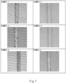
- Fig. 7 shows the results of the observing the samples by the microscope in which the wiring pattern is printed on the surface of the OCA according to Example 1 to Example 6.
- a drawing test was performed using an inkjet printing technique to form a wiring pattern on the surface of the OCA according to Example 7 to Example 13, which were laminated to a TAC substrate KC4UA (available from KONICA MINOLTA, INC. 40 ⁇ m thick).
- a silver nano ink DNS-0169I available from Daicel Corporation was used as the conductive ink material.
- the firing conditions after printing were 120°C, 30 min.
- Table 1 shows the drawing test results of each OCA.
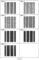
- Fig. 8 shows the results of the observing the samples by the microscope in which the wiring pattern is printed on the surface of the OCA according to Example 7 to Example 13.
- Example 1 to Example 7 are examples, and Example 8 to Example 13 are comparative examples.
- Table 1 in the OCAs according to Example 1 to Example 7 the layer thickness variation after solvent immersion showed low values in both isopropyl alcohol (IPA) and toluene. Thus, it is considered that the drawing test also showed favorable results.
- IPA isopropyl alcohol
- Fig. 7 for example, in the OCA according to Example 7, a wiring pattern without crack and buckling could be formed on the surface of the OCA.
- the layer thickness variation when immersed in isopropyl alcohol (IPA) for 1 minute was greater than 20%.
- the layer thickness variation when immersed in toluene for 1 minute was greater than 18%.
- the OCA eluted when immersed in toluene for 1 minute did not show favorable results for the drawing test.
- Fig. 7 for example, in the OCA according to Example 9 and Example 11, crack and buckling occurred in the wiring pattern formed on the surface of the OCA.
- a wiring-attached adhesive substrate with the wiring formed on OCA (ST75) of Example 1 was used to fabricate a stacked device including the configuration shown in Fig. 3 .
- a different wiring was used for an electronic device on the film.
- a wiring-attached adhesive substrate formed on OCA (ST75) of Example 1 was used to fabricate a stacked device including the configuration shown in Fig. 4 .
- a different wiring was used for an electronic device on the film.
- As the overcoat layer was coated photolec A784-60 (available from SEKISUI CHEMICAL CO., LTD.), which was laminated with PET substrate A4160 (available from TOYOBO Co., Ltd., 125 ⁇ m thick), and adhered through UV curing by irradiation with a light amount of 1000 mj/o.
- a resistance meter terminal was pressed against a wiring section of the wiring-attached adhesive substrate and a conductivity test was performed, the conductivity between the electronic device and the wiring-attached adhesive substrate was confirmed.
- a wiring-attached adhesive substrate formed on OCA (ST75) of Example 1 was used to fabricate a glass stacked body including the configuration shown in Fig. 5 .
- a different wiring was used for an electronic device on the film.
- As the overcoat layer was coated photolec A784-60 (available from SEKISUI CHEMICAL CO., LTD.), which was laminated with PET substrate A4160 (available from TOYOBO Co., Ltd., 125 ⁇ m thick), and adhered by UV curing. PVB sheets (15 mil thick) were adhered to both sides of the laminated film and encapsulated in laminated glass.
- a resistance meter terminal was pressed against a wiring section of the wiring-attached adhesive substrate and a conductivity test was performed, the conductivity between the electronic device and the wiring-attached adhesive substrate was confirmed.
Landscapes
- Engineering & Computer Science (AREA)
- Microelectronics & Electronic Packaging (AREA)
- Chemical & Material Sciences (AREA)
- Manufacturing & Machinery (AREA)
- Dispersion Chemistry (AREA)
- Ceramic Engineering (AREA)
- Inorganic Chemistry (AREA)
- Manufacturing Of Printed Wiring (AREA)
- Laminated Bodies (AREA)
Abstract
To provide a wiring-attached adhesive substrate that can suppress the occurrence of crack and buckling in the wiring pattern formed on the adhesive layer. The wiring-attached adhesive substrate (1) according to one aspect of the present disclosure comprises a substrate (10), an adhesive layer (11) formed on the substrate (10), and a wiring pattern (12) formed on the adhesive layer (11). The adhesive layer (11) has an adhesive strength of 0.01 N/25 mm or more to a PET film, layer thickness variation when the adhesive layer is immersed in isopropyl alcohol for 1 minute is 20% or less, and layer thickness variation when the adhesive layer is immersed in toluene for 1 minute is 18% or less.
Description
- The present disclosure relates to wiring-attached adhesive substrate, stacked device, glass stacked body, and a method for manufacturing wiring attached adhesive substrate.
- Tiling technology is one of the technologies for forming large size electronic devices. Tiling technology is a technology in which a plurality of electronic devices is arrayed on a substrate and adjacent electronic devices are electrically connected to form a large size electronic device. For example, plural display devices are arrayed on a substrate and these display devices can be electrically connected to form a large screen display device.
-
Patent Document 1 discloses a transfer film for forming a transparent conductive layer and a technique for manufacturing a transparent conductive laminate using the transfer film. - Patent Literature 1 :
Japanese Patent No. 5430792 - When configuring an electronic device using tiling technology, it is necessary to array a plurality of electronic devices on a substrate and electrically connect the arrayed electronic devices using wiring. To collectively perform the adhesion between the arrayed electronic devices and electrical connection by wiring, it is useful to use component in which wiring is installed via an adhesive layer on the above-described substrate. As a result, it is necessary to form wiring for electrically connecting a plurality of electronic devices on the adhesive layer that adheres the plurality of electronic devices. In the technique disclosed in
Patent Document 1, a wiring is formed on a substrate for transfer, and a wiring is formed on the adhesive layer by transferring the wiring onto the adhesive layer of the tiling substrate. - However, when such a transfer technique is used, there is a problem that the number of manufacturing step increases, and there is a problem that the auxiliary materials used for manufacturing increase accordingly. Furthermore, when the transfer technique is used, the wiring pattern may collapse when the wiring pattern is transferred onto the adhesive layer.
- As a result, the inventor of the present application has considered a technique for directly forming a wiring pattern on an adhesive layer. However, when the wiring pattern is directly formed on the adhesive layer, a new problem was found that crack and buckling occur in the formed wiring.
- In view of the above-mentioned problems, an object of the present disclosure is to provide a wiring-attached adhesive substrate, a stacked device, and glass stacked body that can suppress the occurrence of crack and buckling in the wiring pattern formed on the adhesive layer, as well as to provide a method for manufacturing the wiring attached adhesive substrate.
- The wiring-attached adhesive substrate according to one aspect of the present disclosure includes a substrate, an adhesive layer formed on the substrate, and a wiring pattern formed on the adhesive layer. The adhesive layer has an adhesive strength of 0.01 N/25 mm or more to a PET film, a layer thickness variation when the adhesive layer is immersed in isopropyl alcohol for 1 minute is 20% or less, and a layer thickness variation when the adhesive layer is immersed in toluene for 1 minute is 18% or less.
- In the wiring-attached adhesive substrate described above, the wiring pattern may be composed of a material containing at least one selected from the group consisting of silver, copper, carbon, and gold.
- In the wiring-attached adhesive substrate described above, a light transmittance of the entire surface of the wiring-attached adhesive substrate may be 50% or more.
- A stacked device according to one aspect of the present disclosure includes a wiring-attached adhesive substrate described above and an electronic device disposed on the wiring-attached adhesive substrate. The electronic device is electrically connected to the wiring pattern formed on the adhesive layer.
- The stacked device described above may further includes an over coat layer covering the electronic device and the wiring pattern.
- A glass stacked body according to one aspect of the present disclosure is a glass stacked body in which the stacked device described above is encapsulated in a glass plate or laminated to the surface of a glass plate.
- A method for manufacturing a wiring-attached adhesive substrate according to one aspect of the present disclosure includes a step of forming an adhesive layer on a substrate and a step of forming a wiring pattern on the adhesive layer using a conductive ink material. The adhesive layer uses a material having an adhesive strength of 0.01 N/25 mm or more to a PET film, a layer thickness variation of 20% or less when the adhesive layer is immersed in isopropyl alcohol for 1 minute, and a layer thickness variation of 18% or less when the adhesive layer is immersed in toluene for 1 minute.
- In the method for manufacturing a wiring-attached adhesive substrate described above, the step of forming a wiring pattern may be a step of printing the conductive ink material on the adhesive layer using inkjet technique to form the wiring pattern.
- In the method for manufacturing a wiring-attached adhesive substrate described above, the step of forming a wiring pattern may be a step of printing the conductive ink material on the adhesive layer using screen printing technique to form the wiring pattern.
- The present disclosure can provide a wiring-attached adhesive substrate, a stacked device, and glass stacked body that can suppress the occurrence of crack and buckling in the wiring pattern formed on the adhesive layer, as well as to provide a method for manufacturing the wiring-attached adhesive substrate.
-
-
Fig. 1 is a cross-sectional view showing a configuration example of a wiring-attached adhesive substrate according to the embodiment; -
Fig. 2 is a plan view showing configuration example of a stacked device according to the embodiment; -
Fig. 3 is a cross-sectional view showing configuration example of a stacked device according to the embodiment; -
Fig. 4 is a cross-sectional view showing configuration example of a stacked device according to the embodiment; -
Fig. 5 is a cross-sectional view showing configuration example of a glass stacked body according to the embodiment; -
Fig. 6 is a cross-sectional view for explaining a method for measuring the layer thickness variation; -
Fig. 7 is microscopically observed photographs of the samples according to Example 1 to Example 6; and -
Fig. 8 is microscopically observed photographs of the samples according to Example 7 to Example 13. - Hereinafter, embodiments will be described with reference to the drawings.
Fig. 1 is a cross-sectional view showing a configuration example of a wiring-attached adhesive substrate according to the embodiment. As shown inFig. 1 , the wiring-attachedadhesive substrate 1 according to the present embodiment includes asubstrate 10,adhesive layer 11, andwiring pattern 12. In addition, in the present specification, thewiring pattern 12 may be simply described aswiring 12. - The
substrate 10 is a component for supporting a plurality of electronic devices 15 (seeFig. 2 ) adhered using theadhesive layer 11. Thesubstrate 10 may be configured with a rigid material or a flexible material. In addition, thesubstrate 10 may be configured using a transparent material, or may be configured using a material having a small retardation value to prevent rainbow unevenness during observation. For example, TAC (Triacetylcellulose), acrylic resin, COP (Cyclo Olefin Polymer), CPI (Colorless and Transparent Polyimide), and the like can be used as thesubstrate 10. - The thickness of the
substrate 10 is, for example, about 12 µm to 250 µm. The thickness of thesubstrate 10 may be changed according to the processability of a post-process such as laminated glass encapsulation. Furthermore, a functional layer may be provided separately on thesubstrate 10. For example, the functional layer is an easy-to-adhere layer, an oxygen barrier layer, a water vapor barrier layer, an invisible layer, an antistatic layer and the like. - The
adhesive layer 11 is formed on thesubstrate 10, and is a component for adhering a plurality of electronic devices 15 (seeFig. 2 ) to thesubstrate 10. For example, a transparent adhesive material, that is, an Optical Clear Adhesive (OCA), can be used for theadhesive layer 11. The thickness of theadhesive layer 11 is, for example, 5 µm to 200 µm. Details of theadhesive layer 11 will be described later. - The
wiring pattern 12 is formed on theadhesive layer 11. For example, thewiring pattern 12 can be formed by drawing directly on theadhesive layer 11. Specifically, thewiring pattern 12 can be formed by printing a conductive ink material on theadhesive layer 11 using inkjet technique. Furthermore, thewiring pattern 12 may be formed by printing the conductive ink material on theadhesive layer 11 using screen printing technique. - For example, the
wiring pattern 12 can be composed of a material containing at least one selected from the group consisting of silver, copper, carbon, and gold. That is, thewiring pattern 12 may be formed using the conductive ink material (wiring ink material) containing at least one selected from the group consisting of silver, copper, carbon, and gold. The wiring width of thewiring pattern 12 is, for example, 1.5 µm to 10 mm. - The wiring-attached
adhesive substrate 1 according to the present embodiment may be transparent. For example, the light transmittance of the entire surface of the wiring-attached adhesive substrate according to the present embodiment may be 50% or more, preferably 60% or more, and more preferably 80% or more. Here, the light transmittance of the entire surface of the wiring-attached adhesive substrate is the average value of the total light transmittance of entire area of the substrate regardless of the installation location of the wiring. - Next, a stacked device in which a plurality of electronic devices is mounted on a wiring-attached adhesive substrate will be described.
Fig. 2 is a plan view illustrating a configuration example of thestacked device 2 according to the embodiment.Fig. 3 is a cross-sectional view illustrating a configuration example of thestacked device 2 according to the embodiment. - As shown in
Figs. 2 and3 , the plurality ofelectronic devices 15 is disposed on the wiring-attachedadhesive substrate 1. Specifically, the plurality ofelectronic devices 15 is adhered to theadhesive layer 11 of the wiring-attachedadhesive substrate 1. As a result, the plurality ofelectronic devices 15 is fixed to thesubstrate 10. At this time theelectronic device 15 is electrically connected to thewiring pattern 12 formed on theadhesive layer 11. For example, theelectronic device 15 is a display device, an optical device, a sensor device, a heating device, and the like, and a connecting component such as Flexible Printed Circuits (FPC) may also be connected. In addition, in the present embodiment, theelectronic device 15 may be an electronic device besides these. - Furthermore, the stacked device according to the present embodiment may include an over
coat layer 16 and asubstrate 17 as shown in thestacked device 3 shown inFig. 4 . The overcoat layer 16 is a component that covers and protects a plurality ofelectronic devices 15 andwiring pattern 12. Specifically, by providing the overcoat layer 16, chemical degradation such as oxidation and corrosion of theelectronic device 15 and thewiring pattern 12 can be suppressed. Furthermore, when the overcoat layer 16 is provided, local pressure is applied to the edge portion or the like where the wiring-attachedadhesive substrate 1 and theelectronic device 15 come into contact, and mechanical degradation such as wire breakage can suppressed. For overcoat layer 16, for example, a curing resin, Optical Clear Resin (OCR), and the like can be used. - The
substrate 17 is a component protecting the plurality ofelectronic devices 15, and can be effectively protected by sandwiching the plurality ofelectronic devices 15 between thelower side substrate 10 and theupper side substrate 17. The same material of as thesubstrate 10 described above can be used for thesubstrate 17. The overcoat layer 16 includes adhesiveness, and thesubstrate 17 can be adhered to the overcoat layer 16 by arranging thesubstrate 17 on the overcoat layer 16. Furthermore, thesubstrate 17 may be separately provided with a functional layer in the same manner as thesubstrate 10. For example, the functional layer is an easy-to-adhere layer, an oxygen barrier layer, a water vapor barrier layer, an invisible layer, an antistatic layer and the like. - Furthermore, in the present embodiment, the
stacked device 3 shown inFig. 4 may be configured to be encapsulated in a glass plate or laminated to a glass plate surface to form a glass stacked body.Fig. 5 is a cross-sectional view showing configuration example of a glass stacked body according to the embodiment.Fig. 5 shows an example in which thelaminating device 3 shown inFig. 4 is encapsulated in a glass plate to form glass stackedbody 4. - The glass stacked
body 4 shown inFig. 5 includesintermediate bonding layers 21a, 21b on the upper surface and the lower surface of thestacked device 3, respectively. For theintermediate bonding layers 21a, 21b, for example, polyvinyl butyral (PVB), ethylene-vinyl acetate copolymer (EVA), and the like can be used. -
Glass plates intermediate bonding layers 21a and 21b. For theglass plates glass plates - For example, when a display device is used as the
electronic device 15, the display device can form a glass stackedbody 4 encapsulated in theglass plates body 4 as a windshield of a vehicle, a windshield with a built-in display device can be configured. In addition, by using such a glass stackedbody 4 for the window glass of a building, a window glass with a built-in display device can be configured. - As described above, in the present embodiment, a
wiring pattern 12 is formed by drawing directly on theadhesive layer 11. For this reason, the characteristics of theadhesive layer 11 are important to suppress the occurrence of crack and buckling of thewiring pattern 12 formed on theadhesive layer 11. Given this point, in the present embodiment, theadhesive layer 11 containing the following characteristics is used. - In the present embodiment, the
adhesive layer 11 has an adhesive strength of 0.01 N/25 mm or more to a PET film. In addition, when thewiring pattern 12 is formed on theadhesive layer 11 using inkjet technique, the adhesive strength of theadhesive layer 11 to the PET film may be 0.01 to 50 N/25 mm. In addition, when thewiring pattern 12 is formed on theadhesive layer 11 using screen printing technique, the adhesive strength of theadhesive layer 11 to the PET film may be 0.01 to 0.20 N/25 mm. That is, when the screen-printing technique is used, it is preferable to weaken the adhesive strength of theadhesive layer 11 compared to the case where the inkjet technique is used. Adhesive strength to PET film can be measured by performing a 180° peel test (sample width 25 mm) using a tensile testing machine. - In addition, in the present embodiment, the material in which the layer thickness variation when the adhesive layer is immersed in isopropyl alcohol (IPA) for 1 minute is 20% or less, and the layer thickness variation when the adhesive layer is immersed in toluene for 1 minute is 18% or less is used for the
adhesive layer 11. At the time, the layer thickness variation when the adhesive layer is immersed in isopropyl alcohol (IPA) for 1 minute is preferably 20% or less, more preferably 14% or less, and still more preferably 7% or less. In addition, the layer thickness variation when the adhesive layer is immersed in toluene for 1 minute is preferably 18% or less, more preferably 13% or less, and still more preferably 11% or less. - Here, as shown in
Fig. 6 , "layer thickness variation" is expressed as (d2 - d1)/d1 × 100(%), where d1 is the thickness of the side surface of theadhesive layer 11 before immersion in the solvent and d2 is the thickness of side surface of theadhesive layer 11 after immersion in the solvent for 1 minute. In addition, for measuring the layer thickness variation, a sample withPET substrate 30 adhered to both sides of theadhesive layer 11 may be used. For a sample that is stacked body, the sample may be used in a state of stacked body, and the cut surface of the sample may be cut out by cutting tool such as a razor blade, tungsten blade, or a diamond knife, or may be processed by ion milling or other processing. - For example, if the
adhesive layer 11 is susceptible to the solvent, when the sample is immersed in the solvent, theadhesive layer 11 is affected by the solvent and theadhesive layer 11 swells. When theadhesive layer 11 swells in this way, the thickness d2 of theadhesive layer 11 after immersion increases, so that the layer thickness variation increases. Furthermore, when the solvent dries some time after immersion, it returns to a state close to the original adhesive layer thickness d1, so that the layer thickness variation of shrinkage after swelling also increases. That is, when the material having a large layer thickness variation is used as theadhesive layer 11, it is susceptible to the influence of solvent, low molecular component, and the like contained in the conductive ink material. For this reason, since swelling and shrinkage of the adhesive layer directly below the wiring after wiring pattern printing occurs largely, it is directly subjected to this dimensional change, and crack and buckling are likely to occur in thewiring pattern 12. In particular, when the solubility of adhesive layer material in the conductive ink solvent is high, the shape of the adhesive layer is collapsed by the elution of the adhesive layer material to the conductive ink, and it is difficult to form a normal wiring on the adhesive layer. For this reason, wiring may be formed including crack and buckling in thewiring pattern 12. - Therefore, in the present embodiment, the material in which the layer thickness variation when the adhesive layer is immersed in isopropyl alcohol (IPA) for 1 minute is 20% or less, and the layer thickness variation when the adhesive layer is immersed in toluene for 1 minute is 18% or less is used for the
adhesive layer 11. If the material containing such characteristics is used for theadhesive layer 11, the solvent contained in the conductive ink material can be suppressed from penetrating into theadhesive layer 11 when thewiring pattern 12 is drawn directly on theadhesive layer 11, thereby suppressing the occurrence of crack and buckling in thewiring pattern 12. - That is, when the
wiring pattern 12 is drawn directly on theadhesive layer 11, dimensional changes caused by swelling of theadhesive layer 11 by the solvent contained in the conductive ink material or shrinkage of theadhesive layer 11 when the solvent dries can be suppressed. Therefore, the occurrence of crack and buckling due to such dimensional changes can be suppressed. - In the present embodiment, isopropyl alcohol is used as a representative of the polar solvent and toluene is used as a representative of the non-polar solvent. That is, a material in which the layer thickness variation when immersed in both a polar solvent and a non-polar solvent satisfies the above conditions is used as the
adhesive layer 11. Theadhesive layer 11 that satisfies the above conditions can be said to be a material with low solvent penetration for a wide range of solvents. Other examples of polar solvents include alcoholic solvents such as methanol, ethanol, 1-propanol, and 1-butanol, ketonic solvents such as methyl ethyl ketone, methyl isobutyl ketone, cyclopentanone, and cyclohexanone, acetate ester solvents such as methyl acetate, ethyl acetate, propyl acetate, and butyl acetate, glycol ether solvents such as propylene glycol monomethyl ether, and propylene glycol monomethyl ether acetate, and other solvents. Other examples of non-polar solvents include hydrocarbon solvents such as xylene, n-hexane, cyclohexane, and benzene. - In the present embodiment, the adhesive layer (OCA) 11 can use a material that satisfies a specific solvent penetration characteristic, such as acryl based, silicone-based, epoxy based, or urethane acrylate based. In addition, the
adhesive layer 11 may have a post-curing characteristic such as thermosetting or UV curability. In addition, theadhesive layer 11 may have characteristics such as softening and adhering when heated (hot melt). - In addition, in the present embodiment, the thickness of the
adhesive layer 11 may be 5 µm to 200 µm. In addition, when thewiring pattern 12 is formed on theadhesive layer 11 using inkjet technique, the thickness of theadhesive layer 11 may be 10 µm to 200 µm. In addition, when thewiring pattern 12 is formed on theadhesive layer 11 using screen printing technique, the thickness of theadhesive layer 11 may be 5 µm to 20 µm. That is, when the screen-printing technique is used, it is preferable to reduce the thickness of theadhesive layer 11 compared to the case where the inkjet technique is used. - In addition, in the present embodiment, a material in which a solvent is dropped onto the adhesive layer and the contact angle after 1 minute is 30° or less, preferably 20° or less, and more preferably 10° or less may be used as the
adhesive layer 11. For the solvent to be dropped, a mixed solvent having a mixing ratio of isopropyl alcohol and toluene of 1:1 can be used. Thus, this small contact angle enables the wiring to be printed with good wettability. - Hereinafter, examples will be described.
- In the following, a wiring pattern drawing test was performed on the samples according to Example 1 to Example 13. Specifically, in addition to investigating the physical characteristics of each OCA (adhesive layer) according to Example 1 to Example 13, a drawing test was performed using screen printing technique or inkjet printing technique. Table 1 shows the maker, product number, and thickness of the samples (OCA) according to Example 1 to Example 13.
- In addition, the adhesive strength of OCA according to Example 1 to Example 13 was measured. Specifically, the 180° peel adhesion strength of OCA when measured at room temperature under conditions of a sample width of 25 mm and a tensile speed of 300 mm/min was measured using an AUTOGRAPH (AG-Xplus) device available from SHIMADZU CORPORATION. Table 1 shows the measured results of the adhesive strength of each OCA.
- In addition, the layer thickness variation after solvent immersion was measured using the following method.
First, as shown inFig. 6 , a measurement sample was prepared in which COSMO SHINE A4160 (available from TOYOBO Co., Ltd., 125 µ thick, one-sided easy adhesion) was laminated to the upper surface and lower surface of the OCA (adhesive layer 11) as aPET substrate 30, respectively, so that the non-easy adhesion surface was on the OCA side. Thereafter, the measurement sample was cut, and the cross-section of the measurement sample was cut out (sectioning) using best replacement blades available from KAI CORPORATION. The size of the measurement sample after cut out was 10 mm × 5 mm. Then, the side surface (cross-section) of the measurement sample was observed by high precision imaging with a laser microscope (LEXT OLS4000, available from OLYMPUS), and the thickness d1 of the OCA before immersion was determined by measuring the average value of the distance between parallel lines at three points. - Next, the measurement sample was immersed in isopropyl alcohol (IPA) for 1 minute. Thereafter, the side surface (cross-section) of the measurement sample after immersion was observed by a laser microscope in the same manner as d1, and the thickness d2 of the OCA after immersion was determined. Then, the layer thickness variation for each OCA was determined using the formula: layer thickness variation = (d2 - d1)/d1 × 100 (%). Similarly, the layer thickness variation when OCA was immersed in toluene was also determined. Table 1 shows measured results of the layer thickness variation of each OCA.
- In addition, a drawing test was performed by forming a wiring pattern on the surface of the OCA according to Example 1 to Example 6 using screen printing technique. For the formation of the wiring pattern, a screen plate for wiring printing and a screen-printing squeegee were used. As the conductive ink material, silver paste RA FS 059 S available from TOYO INK CO., LTD. and silver nano ink S-CS21303 available from GenesInk Co., Ltd. were used. The firing conditions after printing were 120°C, 30 min. Table 1 shows the drawing test results of each OCA.
Fig. 7 shows the results of the observing the samples by the microscope in which the wiring pattern is printed on the surface of the OCA according to Example 1 to Example 6. - In addition, a drawing test was performed using an inkjet printing technique to form a wiring pattern on the surface of the OCA according to Example 7 to Example 13, which were laminated to a TAC substrate KC4UA (available from KONICA MINOLTA, INC. 40 µm thick). A silver nano ink DNS-0169I available from Daicel Corporation was used as the conductive ink material. The firing conditions after printing were 120°C, 30 min. Table 1 shows the drawing test results of each OCA.
Fig. 8 shows the results of the observing the samples by the microscope in which the wiring pattern is printed on the surface of the OCA according to Example 7 to Example 13. -
TABLE 1 SAMPLE OCA MAKER OCA PRODUCT NUMBER OCA THICKNESS [µm] ADHESIVE STRENGTH [N/25mm] LAYER THICKNESS VARIATION AFTER SOLVENT IMMERSION PRINTING METHOD CONDUCTIVE INK DRAWING TEST RESULT IPA TOLUENE EXAMPLE 1 PANAC ST75 8 0.10 1% 0% SCREEN RA FS 059 S OK EXAMPLE 2 PANAC ST75 8 0.10 1% 0% SCREEN S-CS21303 OK EXAMPLE 3 PANAC NT75 8 0.17 1% 0% SCREEN RA FS 059 S OK EXAMPLE 4 PANAC NT75 8 0.17 1% 0% SCREEN S-CS21303 OK EXAMPLE 5 TOKYO FILM SERVICE TKF- 50S 8 0.07 0% 0% SCREEN RA FS 059 S OK EXAMPLE 6 TOKYO FILM SERVICE TKF- 50S 8 0.07 or 0% SCREEN S-CS21303 OK EXAMPLE 7 GUNZE CSA-152 100 13.5 6.8%, 10.2% INKJET DNS-0169I OK EXAMPLE 8 PANAC PDSH2 25 17.1 29.1% ELUTION INKJET DNS-0169I NG EXAMPLE 9 PANAC PDR5 25 16.7 1.2% 19.9% INKJET DNS-0169I NG EXAMPLE 10 PANAC PDC3 25 29.7 24.1% 16.0% INKJET DNS-0169I NG EXAMPLE 11 PANAC PDS1S 25 18.4 34.1% 39.1% INKJET DNS-0169I NG EXAMPLE 12 PANAC PDS1 25 18.5 39.7% ELUTION INKJET DNS-0169I NG EXAMPLE 13 LINTEC MO-T015C 25 25.0 ELUTION ELUTION INKJET DNS-0169I NG - In Table 1, Example 1 to Example 7 are examples, and Example 8 to Example 13 are comparative examples. As shown in Table 1, in the OCAs according to Example 1 to Example 7, the layer thickness variation after solvent immersion showed low values in both isopropyl alcohol (IPA) and toluene. Thus, it is considered that the drawing test also showed favorable results. As shown in
Fig. 7 , for example, in the OCA according to Example 7, a wiring pattern without crack and buckling could be formed on the surface of the OCA. - On the other hand, in the OCA according to Example 8, and Example 10 to Example 12, the layer thickness variation when immersed in isopropyl alcohol (IPA) for 1 minute was greater than 20%. In addition, in the OCA according to Example 13, the OCA eluted when immersed in isopropyl alcohol (IPA) for 1 minute. In addition, in the OCA according to Example 9 and Example 11, the layer thickness variation when immersed in toluene for 1 minute was greater than 18%. In addition, in the OCA according to Example 8, Example 12, and Example 13, the OCA eluted when immersed in toluene for 1 minute. Thus, it is considered that the OCA in Example 8 to Example 13 did not show favorable results for the drawing test. As shown in
Fig. 7 , for example, in the OCA according to Example 9 and Example 11, crack and buckling occurred in the wiring pattern formed on the surface of the OCA. - In addition, a wiring-attached adhesive substrate with the wiring formed on OCA (ST75) of Example 1 was used to fabricate a stacked device including the configuration shown in
Fig. 3 . A different wiring was used for an electronic device on the film. When a resistance meter terminal was pressed against a wiring section of the wiring-attached adhesive substrate and a conductivity test was performed, the conductivity between the electronic device and the wiring-attached adhesive substrate was confirmed. - A wiring-attached adhesive substrate formed on OCA (ST75) of Example 1 was used to fabricate a stacked device including the configuration shown in
Fig. 4 . A different wiring was used for an electronic device on the film. As the overcoat layer was coated photolec A784-60 (available from SEKISUI CHEMICAL CO., LTD.), which was laminated with PET substrate A4160 (available from TOYOBO Co., Ltd., 125 µm thick), and adhered through UV curing by irradiation with a light amount of 1000 mj/o. When a resistance meter terminal was pressed against a wiring section of the wiring-attached adhesive substrate and a conductivity test was performed, the conductivity between the electronic device and the wiring-attached adhesive substrate was confirmed. - A wiring-attached adhesive substrate formed on OCA (ST75) of Example 1 was used to fabricate a glass stacked body including the configuration shown in
Fig. 5 . A different wiring was used for an electronic device on the film. As the overcoat layer was coated photolec A784-60 (available from SEKISUI CHEMICAL CO., LTD.), which was laminated with PET substrate A4160 (available from TOYOBO Co., Ltd., 125 µm thick), and adhered by UV curing. PVB sheets (15 mil thick) were adhered to both sides of the laminated film and encapsulated in laminated glass. When a resistance meter terminal was pressed against a wiring section of the wiring-attached adhesive substrate and a conductivity test was performed, the conductivity between the electronic device and the wiring-attached adhesive substrate was confirmed. - Although the present invention has been described with reference to the above-described embodiments, the present invention is not limited to the configuration of the above-described embodiments, but of course includes various modifications, alterations, and combinations that can be made by a person skilled in the art within the scope of the claimed invention in the claims of this application.
- This application claims priority based on
Japanese Application Patent Application No. 2022-128817, filed August 12, 2022 -
- 1 WIRING-ATTACHED ADHESIVE SUBSTRATE
- 2,3 STACKED DEVICE
- 4 GLASS STACKED BODY
- 10 SUBSTRATE
- 11 ADHESIVE LAYER
- 12 WIRING PATTERN (WIRING)
- 15 ELECTRONIC DEVICE
- 16 OVER COAT LAYER
- 17 SUBSTRATE
- 21a, 21b INTERMEDIATE BONDING LAYER
- 22a, 22b GLASS PLATE
Claims (9)
- A wiring-attached adhesive substrate, comprising:a substrate;an adhesive layer formed on the substrate; andwiring pattern formed on the adhesive layer, whereinthe adhesive layer has an adhesive strength of 0.01 N/25 mm or more to a PET film, a layer thickness variation of 20% or less when the adhesive layer is immersed in isopropyl alcohol for 1 minute, and a layer thickness variation of 18% or less when the adhesive layer is immersed in toluene for 1 minute.
- The wiring-attached adhesive substrate according to claim 1, wherein the wiring pattern is formed of a material comprising at least one selected from the group consisting of silver, copper, carbon, and gold.
- The wiring-attached adhesive substrate according to claim 1 or 2, wherein the light transmittance of the entire surface of the wiring-attached adhesive substrate is 50% or more.
- A stacked device comprising:the wiring-attached adhesive substrate according to claim 1 or 2; andan electronic device disposed on the wiring-attached adhesive substrate, whereinthe electronic device is electrically connected to the wiring pattern formed on the adhesive layer.
- The stacked device according to claim 4, further comprising an over coat layer covering the electronic device and the wiring pattern.
- A glass stacked body in which the stacked device according to claim 4 is encapsulated in a glass plate or laminated to the surface of a glass plate.
- A method for manufacturing a wiring-attached adhesive substrate, comprising:a step of forming an adhesive layer on a substrate,a step of forming a wiring pattern on the adhesive layer using a conductive ink material, whereinthe adhesive layer uses a material having an adhesive strength of 0.01 N/25 mm or more to a PET film, a layer thickness variation when the adhesive layer is immersed in isopropyl alcohol for 1 minute is 20% or less, and a layer thickness variation when the adhesive layer is immersed in toluene for 1 minute is 18% or less.
- The method for manufacturing a wiring-attached adhesive substrate according to claim 7, wherein the step of forming a wiring pattern comprises printing the conductive ink material on the adhesive layer using inkjet technique to form the wiring pattern.
- The method for manufacturing a wiring-attached adhesive substrate according to claim 8, wherein the step of forming a wiring pattern comprises printing the conductive ink material on the adhesive layer using screen printing technique to form the wiring pattern.
Applications Claiming Priority (2)
| Application Number | Priority Date | Filing Date | Title |
|---|---|---|---|
| JP2022128817 | 2022-08-12 | ||
| PCT/JP2023/021103 WO2024034246A1 (en) | 2022-08-12 | 2023-06-07 | Adhesive base material with wiring line, multilayer device, glass laminate, and method for producing adhesive base material with wiring line |
Publications (1)
| Publication Number | Publication Date |
|---|---|
| EP4572538A1 true EP4572538A1 (en) | 2025-06-18 |
Family
ID=89851334
Family Applications (1)
| Application Number | Title | Priority Date | Filing Date |
|---|---|---|---|
| EP23852230.4A Pending EP4572538A1 (en) | 2022-08-12 | 2023-06-07 | Adhesive base material with wiring line, multilayer device, glass laminate, and method for producing adhesive base material with wiring line |
Country Status (5)
| Country | Link |
|---|---|
| US (1) | US20250159795A1 (en) |
| EP (1) | EP4572538A1 (en) |
| JP (1) | JPWO2024034246A1 (en) |
| CN (1) | CN119631576A (en) |
| WO (1) | WO2024034246A1 (en) |
Family Cites Families (9)
| Publication number | Priority date | Publication date | Assignee | Title |
|---|---|---|---|---|
| JP2014045078A (en) * | 2012-08-27 | 2014-03-13 | Senju Metal Ind Co Ltd | Multilayer powder transfer sheet for formation of solder bump |
| JP6279316B2 (en) * | 2012-12-27 | 2018-02-14 | 日本合成化学工業株式会社 | Method for producing acrylic resin for heat-resistant adhesive film |
| JP5430792B1 (en) | 2013-10-09 | 2014-03-05 | 尾池工業株式会社 | Transfer film and method for producing transparent conductive laminate |
| JP2017117568A (en) * | 2015-12-22 | 2017-06-29 | Dic株式会社 | Conductive pattern, electronic circuit, and electromagnetic shield manufacturing method |
| JP6733586B2 (en) * | 2017-03-23 | 2020-08-05 | コニカミノルタ株式会社 | Transparent conductor and method for producing transparent conductor |
| JP6927798B2 (en) * | 2017-08-23 | 2021-09-01 | 信越化学工業株式会社 | Curable perfluoropolyether adhesive composition, adhesives and adhesive tapes using the cured product |
| JP7454772B2 (en) * | 2020-06-29 | 2024-03-25 | Toppanホールディングス株式会社 | Laminate and its manufacturing method |
| JP2022091496A (en) * | 2020-12-09 | 2022-06-21 | 日東電工株式会社 | Manufacturing method of metal pattern laminated substrate |
| JP7380613B2 (en) | 2021-02-24 | 2023-11-15 | トヨタ自動車株式会社 | fuel cell system |
-
2023
- 2023-06-07 CN CN202380054889.9A patent/CN119631576A/en active Pending
- 2023-06-07 JP JP2024540287A patent/JPWO2024034246A1/ja active Pending
- 2023-06-07 EP EP23852230.4A patent/EP4572538A1/en active Pending
- 2023-06-07 WO PCT/JP2023/021103 patent/WO2024034246A1/en not_active Ceased
-
2025
- 2025-01-17 US US19/028,285 patent/US20250159795A1/en active Pending
Also Published As
| Publication number | Publication date |
|---|---|
| US20250159795A1 (en) | 2025-05-15 |
| JPWO2024034246A1 (en) | 2024-02-15 |
| CN119631576A (en) | 2025-03-14 |
| WO2024034246A1 (en) | 2024-02-15 |
Similar Documents
| Publication | Publication Date | Title |
|---|---|---|
| KR101812606B1 (en) | Method for manufacturing transparent printed circuit and method for manufacturing transparent touch panel | |
| CN100383716C (en) | touch panel | |
| EP3125086A1 (en) | Transparent conductive laminated body and touch panel provided with transparent conductive laminated body | |
| WO2017099167A1 (en) | Laminated glass | |
| US20170125136A1 (en) | Transparent electrodes and electronic devices including the same | |
| KR20090037856A (en) | Method for manufacturing display device using glass substrate with protective glass, glass substrate with protective glass and silicone for release paper | |
| KR20130024902A (en) | Method for producing transparent substrate | |
| KR102078438B1 (en) | Metal patterning film and method of preparing the same | |
| TW201723767A (en) | Transparent conductive component with interconnect circuit tab comprising cured organic polymeric material | |
| EP2063685A1 (en) | Plastic glazing | |
| KR102667935B1 (en) | Conductive film and touch panel | |
| JP4126293B2 (en) | Transfer type antenna and manufacturing method thereof | |
| US20250159795A1 (en) | Wiring-attached adhesive substrate, stacked device, glass stacked body, and manufacturing method of wiring-attached adhesive substrate | |
| CN112272815A (en) | Touch sensor module, window stack structure including the same, and image display apparatus including the same | |
| EP3037930A1 (en) | Capacitive touch panel | |
| WO2023080252A1 (en) | Module, laminate for image display device, image display device, module manufacturing method, and wiring board | |
| JP5600458B2 (en) | Manufacturing method of glass plate provided with transfer-type film for baking and fired body | |
| JP5195146B2 (en) | Optical filter for display and manufacturing method thereof | |
| JP7284082B2 (en) | Heater manufacturing method | |
| US20230234883A1 (en) | Glass laminate and method for manufacturing same | |
| US20100086754A1 (en) | Transfer Film for Firing | |
| KR102811344B1 (en) | OPTICAL LAMINATE, transparent display COMPRISING THE SAME, AND MANUFACTURING METHOD FOR THE SAME | |
| KR102964380B1 (en) | OPTICAL LAMINATE, transparent display COMPRISING THE SAME, AND MANUFACTURING METHOD FOR THE SAME | |
| KR20220066110A (en) | Transparent conductive film, laminate and method for manufacturing transparent conductive film | |
| US20100086752A1 (en) | Transfer Films for Firing and Method of Forming Substrate with Functional Pattern |
Legal Events
| Date | Code | Title | Description |
|---|---|---|---|
| STAA | Information on the status of an ep patent application or granted ep patent |
Free format text: STATUS: THE INTERNATIONAL PUBLICATION HAS BEEN MADE |
|
| PUAI | Public reference made under article 153(3) epc to a published international application that has entered the european phase |
Free format text: ORIGINAL CODE: 0009012 |
|
| STAA | Information on the status of an ep patent application or granted ep patent |
Free format text: STATUS: REQUEST FOR EXAMINATION WAS MADE |
|
| 17P | Request for examination filed |
Effective date: 20250220 |
|
| AK | Designated contracting states |
Kind code of ref document: A1 Designated state(s): AL AT BE BG CH CY CZ DE DK EE ES FI FR GB GR HR HU IE IS IT LI LT LU LV MC ME MK MT NL NO PL PT RO RS SE SI SK SM TR |
|
| DAV | Request for validation of the european patent (deleted) | ||
| DAX | Request for extension of the european patent (deleted) |