EP4571855A1 - Method for producing bonded wafer for micro leds - Google Patents
Method for producing bonded wafer for micro leds Download PDFInfo
- Publication number
- EP4571855A1 EP4571855A1 EP23852447.4A EP23852447A EP4571855A1 EP 4571855 A1 EP4571855 A1 EP 4571855A1 EP 23852447 A EP23852447 A EP 23852447A EP 4571855 A1 EP4571855 A1 EP 4571855A1
- Authority
- EP
- European Patent Office
- Prior art keywords
- layer
- micro
- substrate
- led
- gap window
- Prior art date
- Legal status (The legal status is an assumption and is not a legal conclusion. Google has not performed a legal analysis and makes no representation as to the accuracy of the status listed.)
- Pending
Links
Images


Classifications
-
- H—ELECTRICITY
- H10—SEMICONDUCTOR DEVICES; ELECTRIC SOLID-STATE DEVICES NOT OTHERWISE PROVIDED FOR
- H10H—INORGANIC LIGHT-EMITTING SEMICONDUCTOR DEVICES HAVING POTENTIAL BARRIERS
- H10H29/00—Integrated devices, or assemblies of multiple devices, comprising at least one light-emitting semiconductor element covered by group H10H20/00
- H10H29/01—Manufacture or treatment
- H10H29/011—Manufacture or treatment of integrated devices comprising at least one light-emitting semiconductor component covered by group H10H20/00
-
- H—ELECTRICITY
- H10—SEMICONDUCTOR DEVICES; ELECTRIC SOLID-STATE DEVICES NOT OTHERWISE PROVIDED FOR
- H10H—INORGANIC LIGHT-EMITTING SEMICONDUCTOR DEVICES HAVING POTENTIAL BARRIERS
- H10H20/00—Individual inorganic light-emitting semiconductor devices having potential barriers, e.g. light-emitting diodes [LED]
- H10H20/01—Manufacture or treatment
- H10H20/011—Manufacture or treatment of bodies, e.g. forming semiconductor layers
- H10H20/013—Manufacture or treatment of bodies, e.g. forming semiconductor layers having light-emitting regions comprising only Group III-V materials
-
- H—ELECTRICITY
- H10—SEMICONDUCTOR DEVICES; ELECTRIC SOLID-STATE DEVICES NOT OTHERWISE PROVIDED FOR
- H10H—INORGANIC LIGHT-EMITTING SEMICONDUCTOR DEVICES HAVING POTENTIAL BARRIERS
- H10H20/00—Individual inorganic light-emitting semiconductor devices having potential barriers, e.g. light-emitting diodes [LED]
- H10H20/01—Manufacture or treatment
- H10H20/011—Manufacture or treatment of bodies, e.g. forming semiconductor layers
- H10H20/019—Removal of at least a part of a substrate on which semiconductor layers have been formed
-
- H—ELECTRICITY
- H10—SEMICONDUCTOR DEVICES; ELECTRIC SOLID-STATE DEVICES NOT OTHERWISE PROVIDED FOR
- H10H—INORGANIC LIGHT-EMITTING SEMICONDUCTOR DEVICES HAVING POTENTIAL BARRIERS
- H10H20/00—Individual inorganic light-emitting semiconductor devices having potential barriers, e.g. light-emitting diodes [LED]
- H10H20/01—Manufacture or treatment
- H10H20/021—Singulating, e.g. dicing
-
- H—ELECTRICITY
- H10—SEMICONDUCTOR DEVICES; ELECTRIC SOLID-STATE DEVICES NOT OTHERWISE PROVIDED FOR
- H10H—INORGANIC LIGHT-EMITTING SEMICONDUCTOR DEVICES HAVING POTENTIAL BARRIERS
- H10H20/00—Individual inorganic light-emitting semiconductor devices having potential barriers, e.g. light-emitting diodes [LED]
- H10H20/01—Manufacture or treatment
- H10H20/036—Manufacture or treatment of packages
-
- H—ELECTRICITY
- H10—SEMICONDUCTOR DEVICES; ELECTRIC SOLID-STATE DEVICES NOT OTHERWISE PROVIDED FOR
- H10H—INORGANIC LIGHT-EMITTING SEMICONDUCTOR DEVICES HAVING POTENTIAL BARRIERS
- H10H29/00—Integrated devices, or assemblies of multiple devices, comprising at least one light-emitting semiconductor element covered by group H10H20/00
- H10H29/01—Manufacture or treatment
- H10H29/03—Manufacture or treatment using mass transfer of LEDs, e.g. by using liquid suspensions
-
- H—ELECTRICITY
- H10—SEMICONDUCTOR DEVICES; ELECTRIC SOLID-STATE DEVICES NOT OTHERWISE PROVIDED FOR
- H10H—INORGANIC LIGHT-EMITTING SEMICONDUCTOR DEVICES HAVING POTENTIAL BARRIERS
- H10H29/00—Integrated devices, or assemblies of multiple devices, comprising at least one light-emitting semiconductor element covered by group H10H20/00
- H10H29/01—Manufacture or treatment
- H10H29/032—Manufacture or treatment of electrodes
-
- H—ELECTRICITY
- H10—SEMICONDUCTOR DEVICES; ELECTRIC SOLID-STATE DEVICES NOT OTHERWISE PROVIDED FOR
- H10H—INORGANIC LIGHT-EMITTING SEMICONDUCTOR DEVICES HAVING POTENTIAL BARRIERS
- H10H20/00—Individual inorganic light-emitting semiconductor devices having potential barriers, e.g. light-emitting diodes [LED]
- H10H20/01—Manufacture or treatment
- H10H20/032—Manufacture or treatment of electrodes
-
- H—ELECTRICITY
- H10—SEMICONDUCTOR DEVICES; ELECTRIC SOLID-STATE DEVICES NOT OTHERWISE PROVIDED FOR
- H10H—INORGANIC LIGHT-EMITTING SEMICONDUCTOR DEVICES HAVING POTENTIAL BARRIERS
- H10H29/00—Integrated devices, or assemblies of multiple devices, comprising at least one light-emitting semiconductor element covered by group H10H20/00
- H10H29/01—Manufacture or treatment
- H10H29/012—Manufacture or treatment of active-matrix LED displays
Definitions
- the present invention relates to a method for manufacturing a bonded wafer for a micro-LED.
- Patent Document 1 An art to realize displays using micro light emitting diodes (micro-LEDs) is disclosed (Patent Document 1), where GaN-based LEDs are separated from starting substrates using a laser lift-off (LLO) technique and the LEDs are transferred to a mounting substrate, followed by transfer to a drive substrate.
- LLO laser lift-off
- Patent Document 2 While an art compatible with the LLO of LEDs where two electrodes are provided on an upper surface thereon has been disclosed (Patent Document 2), this disclosure pertains to GaN-based LEDs and a configuration thereof is a very typical film thickness structure. This is because a mechanical strength of the GaN-based LED is strong, resulting in few structural requirements for the LLO transferring process conditions.
- a starting substrate of the AlGaInP-based LED is made of GaAs, and the LLO is theoretically impossible with the starting substrate being still attached.
- the starting substrate is removed and an epitaxial layer is transferred to a substrate capable of the LLO, it is possible to enable performing the LLO.
- Patent Document 3 an art for transferring the AlGaInP-based LEDs by etching a sacrificial layer to separate the LEDs from a starting substrate is disclosed.
- Patent Document 4 an art of removing a sacrificial layer and then bonding the LEDs to a support substrate via BCB (adhesive) is disclosed (Patent Document 4) but a structure thereof is not compatible with LLO, and an AlGaInP-based LED structure suitable for the LLO has not been disclosed.
- the AlGaInP-based LEDs have lower mechanical strength compared to the GaN-based LEDs. Therefore, when performing LLO transfer with the AlGaInP-based LEDs having a structure where two electrodes are on the upper surface, a transfer step has a problem in which the LEDs are cracked (destroyed) under the same conditions as in the GaN-based LEDs.
- An object of the present invention is to provide a method for manufacturing a bonded wafer for an AlGaInP-based micro-LED, in which a yield decrease due to a micro-LED cracking during an LLO step is improved.
- the present invention provides a method for manufacturing a bonded wafer for a micro-LED, the method comprising the steps of:
- thermosetting bonding member is preferably at least any of benzocyclobutene, silicone resin, epoxy resin, SOG, polyimide, and amorphous fluororesin.
- thermosetting bonding member With such a thermosetting bonding member, it is possible to reliably perform laser lift-off treatment using an excimer laser.
- the transparent substrate is preferably a sapphire substrate or a quartz substrate.
- the transparent substrate being the to-be-bonded substrate
- this substrate is transparent to the excimer laser, has sufficient thermal strength, and is therefore suitable.
- a method in the step of isolating the epitaxial layer into the micro-LED devices involves forming a pattern by a photolithography method, followed by an ICP etching using chlorine gas and argon gas.
- the transfer substrate is preferably a quartz substrate.
- the quartz substrate can be suitably used as the transfer substrate.
- a method for manufacturing a bonded light-emitting device wafer according to the present invention can be applied to a method for manufacturing a bonded wafer for an AlGaInP-based micro-LED.
- this method even when producing a minute micro-LED device having a quadrilateral shape with a short side length of 50 ⁇ m or less with an AlGaInP-based material which is a material having relatively low strength, the yield decrease caused by the crack of the micro-LED device during the laser lift-off step can be improved by making the GaP window layer as a thick layer having a thickness of 6 ⁇ m or more.
- the present invention is a method for manufacturing a bonded wafer for a micro-LED, the method comprising the steps of:
- an AlGaInP-based light-emitting device structure is formed on a GaAs substrate. Accordingly, as shown in FIG. 1 , an AlGaInP-based first cladding layer 13 having a first conductivity-type, an AlGaInP-based non-doped active layer 14, and an AlGaInP-based second cladding layer 15 having a second conductivity-type are epitaxially grown in sequence on a GaAs substrate 11, being a starting substrate, to form an epitaxial layer. Meanwhile, a GaP window layer 16 is grown on the second cladding layer 15. In this way, each layer is formed to produce an epitaxial wafer 20. More specifically, each layer can be epitaxially grown in the following manner.
- an etching stop layer 12 is epitaxially grown on the first conductivity-type GaAs substrate 11, being the starting substrate.
- the etching stop layer 12 can be formed, for example, after laminating a first conductivity-type GaAs buffer layer, followed by growing a first conductivity-type Ga x In 1-x P (0.4 ⁇ x ⁇ 0.6) first etching stop layer of, e.g., 0.1 ⁇ m, and a first conductivity-type GaAs second etching stop layer of, e.g., 0.1 ⁇ m.
- the epitaxial wafer 20 is provided with a light-emitting device structure 18 as an epitaxial functional layer, in which, for example, a first conductivity-type (Al y Ga 1-y ) x In 1-x P (0.4 ⁇ x ⁇ 0.6, 0.6 ⁇ y ⁇ 1.0) first cladding layer 13 of, e.g., 1.0 ⁇ m, a non-doped (Al y Ga 1-y ) x In 1-x P (0.4 ⁇ x ⁇ 0.6, 0 ⁇ y ⁇ 0.5) active layer 14, a second conductivity-type (Al y Ga 1-y ) x In 1-x P (0.4 ⁇ x ⁇ 0.6, 0.6 ⁇ y ⁇ 1.0) second cladding layer 15 of, e.g., 1.0 ⁇ m, a second conductivity-type Ga x In 1-x P (0.5 ⁇ x ⁇ 1.0) intermediate layer (not shown) of, e.g., 0.1 ⁇ m, and a second conductivity-type GaP window layer 16 are sequentially grown on the etching stop
- the film thicknesses exemplified above are just examples, and the film thickness is no more than a parameter to be changed according to the operating specifications of the device; therefore, the film thickness is not limited to the thickness described here.
- the case where both the first cladding layer 13 and the second cladding layer 15 have a thickness of 1.0 ⁇ m is exemplified, but rated current density of the micro-LED is smaller than that of a discrete LED with a larger size, and even with a thinner film thickness, a function as the cladding layer is not compromised.
- the electrodes are formed as being in contact with the first cladding layer 13, thus it is suitable that the first cladding layer 13 has a thickness of 0.6 ⁇ m or more, considering metal diffusion during ohmic contact formation. A greater thickness than this is preferable and any greater thickness can be selected.
- the second conductivity-type is p-type
- an effective mass of a hole is large, allowing the second cladding layer 15 having a thickness of, for example, about even 0.2 ⁇ m to function in the same way as in a thickness of 1.0 ⁇ m. Therefore, a thickness of 0.2 ⁇ m or more is preferable, and any greater thickness can be selected.
- a concept includes that each layer is not a single composition layer, but has a layer of a plurality of compositions within a range of compositions shown in the example. Furthermore, a concept includes that levels of carrier concentrations are not uniform in each layer but the concentrations have a plurality of levels in each layer.
- the active layer 14 may be composed of a single composition or may have a super-lattice structure where a plurality of barrier layers and active layers are alternatively stacked. Both have the same function and any one of the cases can be selected.
- the GaP window layer 16 is required to have a thickness of 6 ⁇ m or more.
- the thickness thinner than this causes the crack of the micro-LED device during the LLO step described later which results in the decrease in yield.
- any thickness can be selected as the upper limit of the thickness of the GaP window layer 16 as long as the thickness thereof is within a thickness range that is thinner than a short side length at device isolation described later.
- the GaP window layer 16 is bonded to a transparent substrate 30, being a to-be-bonded substrate transparent to visible light and ultraviolet light, via a thermosetting bonding member 25.
- This bonding can be specifically performed as follows. Benzocyclobutene (BCB), for example, is spin-coated as the thermosetting bonding member 25 on the epitaxial wafer 20.
- the transparent substrate 30 (for example, sapphire substrate), being the to-be-bonded substrate, is then stacked facing each other and bonded by thermocompression. This produces an epitaxial-bonded substrate by bonding the epitaxial wafer and the transparent substrate 30 (sapphire substrate) via BCB.
- BCB is coated by spin coating, a designed film thickness can be, for example, 0.6 ⁇ m.
- the transparent substrate 30, being the to-be-bonded substrate is not limited to the sapphire substrate, and any material can be selected as long as being transparent to visible light and ultraviolet light and flatness are guaranteed. Quartz can be selected instead of sapphire.
- thermosetting bonding member 25 is not limited to BCB, any material that is suitable for a laser process described later, i.e., a material transparent to visible light and absorbing ultraviolet light can be selected.
- BCB silicone resin, epoxy resin, SOG (Spin On Glass, spin-on-glass), polyimide (PI, Polyimide), and amorphous fluororesin such as CYTOP (registered trademark) can be used.
- thermosetting bonding member 25 such as BCB
- the thermosetting bonding member 25 can be patterned into an isolated island shape, a line shape, or other shapes, and a bonding step is then performed, and the same result can be obtained.
- the thickness of the thermosetting bonding member 25 is not limited to 0.6 ⁇ m; even with the thinner thickness, the same effect can be obtained.
- the GaAs substrate 11 being the starting substrate, is separated.
- the more specific description is as follows.
- the GaAs substrate can be separated and removed by wet etching with ammonia-hydrogen peroxide mixture (a mixed solution of ammonia and hydrogen peroxide). This exposes a GaInP first etching stop layer out of the etching stop layer 12.
- the etchant is switched to a hydrochloric acid-based etchant to selectively remove the GaInP first etching stop layer out of the etching stop layer 12, and then the GaAs second etching stop layer out of the etching stop layer 12 is exposed.
- the etchant is switched to a peroxide sulfuric-based etchant (a mixed solution of sulfuric acid and hydrogen peroxide) to selectively remove the GaAs second etching stop layer, thereby exposing the first cladding layer 13.
- a peroxide sulfuric-based etchant a mixed solution of sulfuric acid and hydrogen peroxide
- the epitaxial layer is isolated into the micro-LED devices having a quadrilateral shape with a short side length of 50 ⁇ m or less.
- the second cladding layer 15 or the GaP window layer 16 in a partial region of the micro-LED device is exposed.
- This device isolation processing step is preferably performed by forming a pattern using a photolithography method and by an ICP (inductively coupled plasma, Inductively Coupled Plasma) etching using chlorine gas and argon gas (device isolation groove 47 in FIG. 4 ).
- the ICP process can be performed twice; the step of exposing the BCB layer (thermosetting bonding member 25), and the step of exposing the second cladding layer 15 or the GaP window layer 16.
- the size of the device isolation here can be, for example, 25 ⁇ m ⁇ 50 ⁇ m but this is just an example, and the present invention exhibits a remarkable effect on the minute micro-LED device having a quadrilateral shape with a short side length of 50 ⁇ m or less.
- the GaP window layer 16 preferably has a thickness less than or equal to the short side length of the device isolation (when the size of the micro-LED device by the above device isolation is 25 ⁇ m ⁇ 50 ⁇ m, the thickness is 25 ⁇ m or less).
- the reason thereof is that, although the LLO step itself is possible even when the GaP window layer 16 has a thickness of more than 25 ⁇ m, the micro-LED device is likely to fall over after the LLO when the GaP window layer 16 has a thickness thicker than the short side length. Consequently, even when the yield due to the crack of the micro-LED device is improved, a risk in which a transfer yield is decreased due to the falling over of the micro-LED device. Therefore, it is suitable to maintain a height of the GaP window layer 16 at or below the short side length.
- the second cladding layer 15 is exposed; however, this is not limited to the case where the second cladding layer 15 is exposed. It is sufficient for the active layer 14 to be at least separated, and the same effect can be obtained even when the GaP window layer 16, rather than the second cladding layer 15, is exposed.
- a protective film 52 can be formed as end face processing, as shown in FIG. 5 .
- SiO 2 can be used as the protective film 52.
- the protective film 52 is not limited to SiO 2 , but any material can be selected as long as the end face can be protected and the material has insulating properties. SiN x , titanium oxide, magnesium oxide, etc., can also be selected.
- a first electrodes 54 in contact with the layer having the first conductivity-type and a second electrode 56 in contact with the layer having the second conductive-type are formed, and ohmic contact is then formed by performing heat treatment.
- the first conductivity-type is designed as n-type
- the second conductivity-type is designed as p-type
- metals containing Au and Si can be used for the electrode in contact with the n-type layer
- metals containing Au and Be can be used for the electrode in contact with the p-type layer.
- the metals for the n-type electrode are not limited to Au and Si, and the same result can be obtained by using metals containing Au and Ge.
- the metals for the p-type electrode are not limited to Au and Be, and the same result can be obtained by using metals containing Au and Zn.
- the first electrode 54 and the second electrode 56 are adhered to a transfer substrate 70 via silicone resin 65.
- a quartz substrate is suitable for the transfer substrate 70.
- the transfer substrate 70 and the ohmic electrodes are faced each other, and the pressure is applied, then the ohmic electrodes portion (the first electrode 54 and the second electrode 56) can be adhered to the silicone resin 65.
- thermosetting bonding member 25 in contact with the transparent substrate 30 is sublimated by laser lift-off treatment, causing the micro-LED device isolated from the transparent substrate 30, thereby manufacturing the bonded wafer for a micro-LED ( FIG. 9 ).
- an excimer laser is irradiated from the transparent substrate 30 side, such as the sapphire substrate.
- a layer of the thermosetting bonding member 25, such as BCB layer in contact with the transparent substrate 30, is sublimated by laser lift-off (LLO) treatment, causing the micro-LED device isolated from the transparent substrate 30.
- LLO laser lift-off
- thermosetting bonding member 25 such as the BCB, remaining on the micro-LED device surface can be removed by ashing or plasma etching.
- an etching stop layer 12 was made on an n-type (first conductivity-type) GaAs substrate 11, being a starting substrate, after stacking an n-type GaAs buffer layer, followed by epitaxially growing an n-type GaInP first etching stop layer of 0.1 ⁇ m thickness, and an n-type GaAs second etching stop layer of 0.1 ⁇ m thickness.
- an epitaxial wafer 20 was provided with a light emitting device structure 18 as an epitaxial functional layer, in which an n-type (Al y Ga 1-y ) x In 1-x P (0.4 ⁇ x ⁇ 0.6, 0.6 ⁇ y ⁇ 1.0) first cladding layer 13 of 1.0 ⁇ m thickness, a non-doped (Al y Ga 1-y ) x In 1-x P (0.4 ⁇ x ⁇ 0.6, 0 ⁇ y ⁇ 0.5) active layer 14, a p-type (Al y Ga 1-y ) x In 1-x P (0.4 ⁇ x ⁇ 0.6, 0.6 ⁇ y ⁇ 1.0) second cladding layer 15 of 1.0 ⁇ m thickness, a p-type Ga x In 1-x P (0.5 ⁇ x ⁇ 1.0) intermediate layer (not shown) of 0.1 ⁇ m thickness, and a p-type GaP window layer 16 were sequentially grown ( FIG. 1 ). At this point, the thickness of the GaP window layer 16 was varied in a range of 2 to 5 ⁇ m (Compar
- benzocyclobutene (BCB) was spin-coated as a thermosetting bonding member 25 on the epitaxial wafer 20 (on the light emitting device structure 18).
- BCB was coated by spin coating, a designed film thickness was set to 0.6 ⁇ m.
- the GaAs substrate 11, being the starting substrate, and the etching stop layer 12 were removed by wet etching to produce an epitaxial bonded substrate.
- a pattern was formed using a photolithography method, followed by an ICP using chlorine gas and argon gas to perform device isolation processing of 50 ⁇ 100 ⁇ m (device isolation groove 47).
- the ICP processing was performed twice; the step of exposing the BCB layer 25, and the step of exposing the second cladding layer 15.
- a SiO 2 protective film 52 was formed as end face processing, as shown in FIG. 5 .
- a first electrode 54 and a second electrode 56 in contact with an n-type layer and a p-type layer were formed, respectively, and ohmic contact was then formed by performing heat treatment.
- an excimer laser was irradiated from a side of the transparent substrate 30 made of sapphire, and the BCB layer portion in contact with the sapphire substrate was sublimated by laser lift-off (LLO) treatment, causing the sapphire substrate and micro-LED dice isolated ( FIG. 9 ). Furthermore, BCB was removed, as shown in FIG. 10 .
- LLO laser lift-off
- FIG. 11 shows the results of an investigation for yields of each wafer in which the Gap window layers 16 have different thicknesses.
- the GaP window layer 16 had a thickness of 4 ⁇ m or less (Comparative Example)
- all micro-LED devices were cracked and the yields thereof were 0.
- the thickness of the GaP window layer 16 was 5 ⁇ m (Comparative Example)
- a good yield rate was improved but still insufficient.
- the thickness of the GaP window layer 16 was 6 ⁇ m (Example)
- the good yield rate reached 80% or higher
- the thickness of the GaP window layer 16 was 8 ⁇ m or higher (Example)
- cracking was eliminated, resulting in a 100% yield.
- the present description includes the following embodiments.
Landscapes
- Led Devices (AREA)
- Semiconductor Lasers (AREA)
Abstract
The present invention is a method for manufacturing a bonded wafer for a micro-LED, the method includes the steps of epitaxially growing an AlGaInP-based first cladding layer, non-doped active layer, and second cladding layer on a GaAs substrate to form an epitaxial layer, growing a GaP window layer on the second cladding layer, bonding the GaP window layer to a transparent substrate via a thermosetting bonding member, separating the GaAs substrate, isolating the epitaxial layer into micro-LED devices, exposing the second cladding layer or the GaP window layer of the micro-LED device, forming electrodes, adhering the electrodes to a transfer substrate, and irradiating a laser from the transparent substrate side to isolate the micro-LED device from the transparent substrate, in which the GaP window layer has a thickness of 6 µm or more. This provides a method for manufacturing a bonded wafer for an AlGaInP-based micro-LED which improves a yield decrease caused by a crack in a micro-LED device during a LLO step.
Description
- The present invention relates to a method for manufacturing a bonded wafer for a micro-LED.
- An art to realize displays using micro light emitting diodes (micro-LEDs) is disclosed (Patent Document 1), where GaN-based LEDs are separated from starting substrates using a laser lift-off (LLO) technique and the LEDs are transferred to a mounting substrate, followed by transfer to a drive substrate.
- While an art compatible with the LLO of LEDs where two electrodes are provided on an upper surface thereon has been disclosed (Patent Document 2), this disclosure pertains to GaN-based LEDs and a configuration thereof is a very typical film thickness structure. This is because a mechanical strength of the GaN-based LED is strong, resulting in few structural requirements for the LLO transferring process conditions.
- On the other hand, no art of LLO using AlGaInP-based LED has been disclosed. A starting substrate of the AlGaInP-based LED is made of GaAs, and the LLO is theoretically impossible with the starting substrate being still attached. However, when the starting substrate is removed and an epitaxial layer is transferred to a substrate capable of the LLO, it is possible to enable performing the LLO.
- While the art of LLO is not applied, as an art for transferring the AlGaInP-based LEDs by etching a sacrificial layer to separate the LEDs from a starting substrate is disclosed (Patent Document 3). Moreover, an art of removing a sacrificial layer and then bonding the LEDs to a support substrate via BCB (adhesive) is disclosed (Patent Document 4) but a structure thereof is not compatible with LLO, and an AlGaInP-based LED structure suitable for the LLO has not been disclosed.
- The AlGaInP-based LEDs have lower mechanical strength compared to the GaN-based LEDs. Therefore, when performing LLO transfer with the AlGaInP-based LEDs having a structure where two electrodes are on the upper surface, a transfer step has a problem in which the LEDs are cracked (destroyed) under the same conditions as in the GaN-based LEDs.
-
- Patent Document 1:
JP 2020-521181 A - Patent Document 2:
JP 2015-2324 A - Patent Document 3:
JP 2021-153186 A - Patent Document 4:
JP 2006-32952 A - The present invention has been made in view of the above-described problem. An object of the present invention is to provide a method for manufacturing a bonded wafer for an AlGaInP-based micro-LED, in which a yield decrease due to a micro-LED cracking during an LLO step is improved.
- To achieve the object, the present invention provides a method for manufacturing a bonded wafer for a micro-LED, the method comprising the steps of:
- epitaxially growing an AlGaInP-based first cladding layer having a first conductivity-type, an AlGaInP-based non-doped active layer, and an AlGaInP-based second cladding layer having a second conductivity-type on a GaAs substrate to form an epitaxial layer;
- growing a GaP window layer on the second cladding layer;
- bonding the GaP window layer to a transparent substrate, being a to-be-bonded substrate transparent to visible light and ultraviolet light, via a thermosetting bonding member;
- separating the GaAs substrate;
- isolating the epitaxial layer into micro-LED devices each having a quadrilateral shape with a short side length of 50 µm or less;
- exposing the second cladding layer or the GaP window layer in a partial region of the micro-LED device;
- forming a first electrode in contact with a layer having the first conductivity-type and a second electrode in contact with a layer having the second conductivity-type, and performing heat treatment to form an ohmic contact;
- adhering the first electrode and the second electrode to a transfer substrate via silicone resin; and
- irradiating a laser from the transparent substrate side and sublimating the thermosetting bonding member in contact with the transparent substrate through laser lift-off treatment to isolate the micro-LED device from the transparent substrate, wherein
- the GaP window layer has a thickness of 6 µm or more.
- In this way, by making a thickness of the GaP window layer 6 µm or more, even a minute AlGaInP-based micro-LED device having a quadrilateral shape with a short side length of 50 µm or less can suppress cracking during laser lift-off treatment and improve a yield decrease.
- In this case, the thermosetting bonding member is preferably at least any of benzocyclobutene, silicone resin, epoxy resin, SOG, polyimide, and amorphous fluororesin.
- With such a thermosetting bonding member, it is possible to reliably perform laser lift-off treatment using an excimer laser.
- In addition, the transparent substrate is preferably a sapphire substrate or a quartz substrate.
- When the transparent substrate, being the to-be-bonded substrate, is made of sapphire or quartz, this substrate is transparent to the excimer laser, has sufficient thermal strength, and is therefore suitable.
- Moreover, it is preferable that a method in the step of isolating the epitaxial layer into the micro-LED devices involves forming a pattern by a photolithography method, followed by an ICP etching using chlorine gas and argon gas.
- According to such a method, device isolation can be achieved relatively easily and reliably.
- In addition, the transfer substrate is preferably a quartz substrate.
- In the inventive method for manufacturing a bonded wafer for a micro-LED, the quartz substrate can be suitably used as the transfer substrate.
- A method for manufacturing a bonded light-emitting device wafer according to the present invention can be applied to a method for manufacturing a bonded wafer for an AlGaInP-based micro-LED. In this method, even when producing a minute micro-LED device having a quadrilateral shape with a short side length of 50 µm or less with an AlGaInP-based material which is a material having relatively low strength, the yield decrease caused by the crack of the micro-LED device during the laser lift-off step can be improved by making the GaP window layer as a thick layer having a thickness of 6 µm or more.
-
-
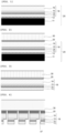
FIG. 1 is a schematic cross-sectional view illustrating a part of a method for manufacturing a bonded wafer for a micro-LED according to the present invention. -
FIG. 2 is a schematic cross-sectional view illustrating another part of a method for manufacturing a bonded wafer for a micro-LED according to the present invention. -
FIG. 3 is a schematic cross-sectional view illustrating another part of a method for manufacturing a bonded wafer for a micro-LED according to the present invention. -
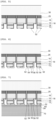
FIG. 4 is a schematic cross-sectional view illustrating another part of a method for manufacturing a bonded wafer for a micro-LED according to the present invention. -
FIG. 5 is a schematic cross-sectional view illustrating another part of a method for manufacturing a bonded wafer for a micro-LED according to the present invention. -
FIG. 6 is a schematic cross-sectional view illustrating another part of a method for manufacturing a bonded wafer for a micro-LED according to the present invention. -
FIG. 7 is a schematic cross-sectional view illustrating another part of a method for manufacturing a bonded wafer for a micro-LED according to the present invention. -
FIG. 8 is a schematic cross-sectional view illustrating another part of a method for manufacturing a bonded wafer for a micro-LED according to the present invention. -
FIG. 9 is a schematic cross-sectional view illustrating another part of a method for manufacturing a bonded wafer for a micro-LED according to the present invention. -
FIG. 10 is a schematic cross-sectional view illustrating another part of a method for manufacturing a bonded wafer for a micro-LED according to the present invention. -
FIG. 11 is a graph illustrating yield results for each wafer having different GaP window layer thicknesses of bonded wafers for micro-LEDs manufactured in Example and Comparative Example. - Hereinafter, the present invention will be described in detail. However, the present invention is not limited thereto.
- The present invention is a method for manufacturing a bonded wafer for a micro-LED, the method comprising the steps of:
- epitaxially growing an AlGaInP-based first cladding layer having a first conductivity-type, an AlGaInP-based non-doped active layer, and an AlGaInP-based second cladding layer having a second conductivity-type on a GaAs substrate to form an epitaxial layer;
- growing a GaP window layer on the second cladding layer;
- bonding the GaP window layer to a transparent substrate, being a to-be-bonded substrate transparent to visible light and ultraviolet light, via a thermosetting bonding member;
- separating the GaAs substrate;
- isolating the epitaxial layer into micro-LED devices each having a quadrilateral shape with a short side length of 50 µm or less;
- exposing the second cladding layer or the GaP window layer in a partial region of the micro-LED device;
- forming a first electrode in contact with a layer having the first conductivity-type and a second electrode in contact with a layer having the second conductivity-type, and performing heat treatment to form an ohmic contact;
- adhering the first electrode and the second electrode to a transfer substrate via silicone resin; and
- irradiating a laser from the transparent substrate side and sublimating the thermosetting bonding member in contact with the transparent substrate through laser lift-off treatment to isolate the micro-LED device from the transparent substrate, wherein
- the GaP window layer has a thickness of 6 µm or more.
- Hereinafter, the aspects of the present invention will be described, referring to the drawings.
- First, an AlGaInP-based light-emitting device structure is formed on a GaAs substrate. Accordingly, as shown in
FIG. 1 , an AlGaInP-basedfirst cladding layer 13 having a first conductivity-type, an AlGaInP-based non-dopedactive layer 14, and an AlGaInP-basedsecond cladding layer 15 having a second conductivity-type are epitaxially grown in sequence on aGaAs substrate 11, being a starting substrate, to form an epitaxial layer. Meanwhile, aGaP window layer 16 is grown on thesecond cladding layer 15. In this way, each layer is formed to produce anepitaxial wafer 20. More specifically, each layer can be epitaxially grown in the following manner. - As shown in
FIG. 1 , anetching stop layer 12 is epitaxially grown on the first conductivity-type GaAs substrate 11, being the starting substrate. Theetching stop layer 12 can be formed, for example, after laminating a first conductivity-type GaAs buffer layer, followed by growing a first conductivity-type GaxIn1-xP (0.4≤x≤0.6) first etching stop layer of, e.g., 0.1 µm, and a first conductivity-type GaAs second etching stop layer of, e.g., 0.1 µm. Moreover, theepitaxial wafer 20 is provided with a light-emittingdevice structure 18 as an epitaxial functional layer, in which, for example, a first conductivity-type (AlyGa1-y)xIn1-xP (0.4≤x≤0.6, 0.6≤y≤1.0)first cladding layer 13 of, e.g., 1.0 µm, a non-doped (AlyGa1-y)xIn1-xP (0.4≤x≤0.6, 0≤y≤0.5)active layer 14, a second conductivity-type (AlyGa1-y)xIn1-xP (0.4≤x≤0.6, 0.6≤y≤1.0)second cladding layer 15 of, e.g., 1.0 µm, a second conductivity-type GaxIn1-xP (0.5≤x≤1.0) intermediate layer (not shown) of, e.g., 0.1 µm, and a second conductivity-typeGaP window layer 16 are sequentially grown on theetching stop layer 12. At this point, from thefirst cladding layer 13 to thesecond cladding layer 15 is referred to as a double-hetero (DH) structure part (FIG. 1 ). - The film thicknesses exemplified above are just examples, and the film thickness is no more than a parameter to be changed according to the operating specifications of the device; therefore, the film thickness is not limited to the thickness described here. The case where both the
first cladding layer 13 and thesecond cladding layer 15 have a thickness of 1.0 µm is exemplified, but rated current density of the micro-LED is smaller than that of a discrete LED with a larger size, and even with a thinner film thickness, a function as the cladding layer is not compromised. - As described later, the electrodes are formed as being in contact with the
first cladding layer 13, thus it is suitable that thefirst cladding layer 13 has a thickness of 0.6 µm or more, considering metal diffusion during ohmic contact formation. A greater thickness than this is preferable and any greater thickness can be selected. - When the second conductivity-type is p-type, an effective mass of a hole is large, allowing the
second cladding layer 15 having a thickness of, for example, about even 0.2 µm to function in the same way as in a thickness of 1.0 µm. Therefore, a thickness of 0.2 µm or more is preferable, and any greater thickness can be selected. - Moreover, a concept includes that each layer is not a single composition layer, but has a layer of a plurality of compositions within a range of compositions shown in the example. Furthermore, a concept includes that levels of carrier concentrations are not uniform in each layer but the concentrations have a plurality of levels in each layer.
- The
active layer 14 may be composed of a single composition or may have a super-lattice structure where a plurality of barrier layers and active layers are alternatively stacked. Both have the same function and any one of the cases can be selected. - In the present invention, the
GaP window layer 16 is required to have a thickness of 6 µm or more. The thickness thinner than this causes the crack of the micro-LED device during the LLO step described later which results in the decrease in yield. Moreover, any thickness can be selected as the upper limit of the thickness of theGaP window layer 16 as long as the thickness thereof is within a thickness range that is thinner than a short side length at device isolation described later. - Next, as shown in
FIG. 2 , theGaP window layer 16 is bonded to atransparent substrate 30, being a to-be-bonded substrate transparent to visible light and ultraviolet light, via athermosetting bonding member 25. This bonding can be specifically performed as follows. Benzocyclobutene (BCB), for example, is spin-coated as thethermosetting bonding member 25 on theepitaxial wafer 20. The transparent substrate 30 (for example, sapphire substrate), being the to-be-bonded substrate, is then stacked facing each other and bonded by thermocompression. This produces an epitaxial-bonded substrate by bonding the epitaxial wafer and the transparent substrate 30 (sapphire substrate) via BCB. When BCB is coated by spin coating, a designed film thickness can be, for example, 0.6 µm. - Note that the
transparent substrate 30, being the to-be-bonded substrate, is not limited to the sapphire substrate, and any material can be selected as long as being transparent to visible light and ultraviolet light and flatness are guaranteed. Quartz can be selected instead of sapphire. - In addition, the
thermosetting bonding member 25 is not limited to BCB, any material that is suitable for a laser process described later, i.e., a material transparent to visible light and absorbing ultraviolet light can be selected. Other than BCB, silicone resin, epoxy resin, SOG (Spin On Glass, spin-on-glass), polyimide (PI, Polyimide), and amorphous fluororesin such as CYTOP (registered trademark) can be used. - Moreover, in addition to being applied in a layered shape, the
thermosetting bonding member 25, such as BCB, can be patterned into an isolated island shape, a line shape, or other shapes, and a bonding step is then performed, and the same result can be obtained. Moreover, the thickness of thethermosetting bonding member 25 is not limited to 0.6 µm; even with the thinner thickness, the same effect can be obtained. - Then, as shown in
FIG. 3 , theGaAs substrate 11, being the starting substrate, is separated. The more specific description is as follows. The GaAs substrate can be separated and removed by wet etching with ammonia-hydrogen peroxide mixture (a mixed solution of ammonia and hydrogen peroxide). This exposes a GaInP first etching stop layer out of theetching stop layer 12. Then the etchant is switched to a hydrochloric acid-based etchant to selectively remove the GaInP first etching stop layer out of theetching stop layer 12, and then the GaAs second etching stop layer out of theetching stop layer 12 is exposed. Then, the etchant is switched to a peroxide sulfuric-based etchant (a mixed solution of sulfuric acid and hydrogen peroxide) to selectively remove the GaAs second etching stop layer, thereby exposing thefirst cladding layer 13. By performing the above treatments, an epitaxial bonded substrate that retains only the DH layer and the GaP window layer can be produced. - Next, as shown in
FIG. 4 , the epitaxial layer is isolated into the micro-LED devices having a quadrilateral shape with a short side length of 50 µm or less. In addition, thesecond cladding layer 15 or theGaP window layer 16 in a partial region of the micro-LED device is exposed. This device isolation processing step is preferably performed by forming a pattern using a photolithography method and by an ICP (inductively coupled plasma, Inductively Coupled Plasma) etching using chlorine gas and argon gas (device isolation groove 47 inFIG. 4 ). The ICP process can be performed twice; the step of exposing the BCB layer (thermosetting bonding member 25), and the step of exposing thesecond cladding layer 15 or theGaP window layer 16. - The size of the device isolation here can be, for example, 25 µm×50 µm but this is just an example, and the present invention exhibits a remarkable effect on the minute micro-LED device having a quadrilateral shape with a short side length of 50 µm or less. Moreover, the
GaP window layer 16 preferably has a thickness less than or equal to the short side length of the device isolation (when the size of the micro-LED device by the above device isolation is 25 µm×50 µm, the thickness is 25 µm or less). The reason thereof is that, although the LLO step itself is possible even when theGaP window layer 16 has a thickness of more than 25 µm, the micro-LED device is likely to fall over after the LLO when theGaP window layer 16 has a thickness thicker than the short side length. Consequently, even when the yield due to the crack of the micro-LED device is improved, a risk in which a transfer yield is decreased due to the falling over of the micro-LED device. Therefore, it is suitable to maintain a height of theGaP window layer 16 at or below the short side length. - In
FIG. 4 , an example is provided where thesecond cladding layer 15 is exposed; however, this is not limited to the case where thesecond cladding layer 15 is exposed. It is sufficient for theactive layer 14 to be at least separated, and the same effect can be obtained even when theGaP window layer 16, rather than thesecond cladding layer 15, is exposed. - After the device isolation processing in
FIG. 4 , aprotective film 52 can be formed as end face processing, as shown inFIG. 5 . SiO2 can be used as theprotective film 52. In addition, theprotective film 52 is not limited to SiO2, but any material can be selected as long as the end face can be protected and the material has insulating properties. SiNx, titanium oxide, magnesium oxide, etc., can also be selected. - Following the formation of the
protective film 52, as shown inFIG. 6 , afirst electrodes 54 in contact with the layer having the first conductivity-type and asecond electrode 56 in contact with the layer having the second conductive-type are formed, and ohmic contact is then formed by performing heat treatment. For example, the first conductivity-type is designed as n-type, and the second conductivity-type is designed as p-type; metals containing Au and Si can be used for the electrode in contact with the n-type layer, and metals containing Au and Be can be used for the electrode in contact with the p-type layer. - The metals for the n-type electrode are not limited to Au and Si, and the same result can be obtained by using metals containing Au and Ge. Moreover, the metals for the p-type electrode are not limited to Au and Be, and the same result can be obtained by using metals containing Au and Zn.
- After forming the ohmic contact, as shown in
FIG. 7 , thefirst electrode 54 and thesecond electrode 56 are adhered to atransfer substrate 70 viasilicone resin 65. A quartz substrate is suitable for thetransfer substrate 70. For example, as shown inFIG. 7 , by using thetransfer substrate 70 on whichsilicone resin 65 is applied to form a convex pattern, thetransfer substrate 70 and the ohmic electrodes (thefirst electrode 54 and the second electrode 56) are faced each other, and the pressure is applied, then the ohmic electrodes portion (thefirst electrode 54 and the second electrode 56) can be adhered to thesilicone resin 65. - Next, as shown in
FIG. 8 , a laser (indicated by six single-headed arrows inFIG. 7 ) is irradiated from thetransparent substrate 30 side. Then, thethermosetting bonding member 25 in contact with thetransparent substrate 30 is sublimated by laser lift-off treatment, causing the micro-LED device isolated from thetransparent substrate 30, thereby manufacturing the bonded wafer for a micro-LED (FIG. 9 ). In this way, for example, an excimer laser is irradiated from thetransparent substrate 30 side, such as the sapphire substrate. Then, a layer of thethermosetting bonding member 25, such as BCB layer in contact with thetransparent substrate 30, is sublimated by laser lift-off (LLO) treatment, causing the micro-LED device isolated from thetransparent substrate 30. - After isolating the micro-LED device and the
transparent substrate 30, such as the sapphire substrate, as shown inFIG. 10 , thethermosetting bonding member 25, such as the BCB, remaining on the micro-LED device surface can be removed by ashing or plasma etching. - Hereinafter, the present invention will be described in detail with reference to Example and Comparative Example. However, the present invention is not limited thereto.
- First, as shown in
FIG. 1 , anetching stop layer 12 was made on an n-type (first conductivity-type)GaAs substrate 11, being a starting substrate, after stacking an n-type GaAs buffer layer, followed by epitaxially growing an n-type GaInP first etching stop layer of 0.1 µm thickness, and an n-type GaAs second etching stop layer of 0.1 µm thickness. Moreover, anepitaxial wafer 20 was provided with a light emittingdevice structure 18 as an epitaxial functional layer, in which an n-type (AlyGa1-y)xIn1-xP (0.4≤x≤0.6, 0.6≤y≤1.0)first cladding layer 13 of 1.0 µm thickness, a non-doped (AlyGa1-y)xIn1-xP (0.4≤x≤0.6, 0≤y≤0.5)active layer 14, a p-type (AlyGa1-y)xIn1-xP (0.4≤x≤0.6, 0.6≤y≤1.0)second cladding layer 15 of 1.0 µm thickness, a p-type GaxIn1-xP (0.5≤x≤1.0) intermediate layer (not shown) of 0.1 µm thickness, and a p-typeGaP window layer 16 were sequentially grown (FIG. 1 ). At this point, the thickness of theGaP window layer 16 was varied in a range of 2 to 5 µm (Comparative Example) and 6 to 15 µm (Example). - Then, as shown in
FIG. 2 , benzocyclobutene (BCB) was spin-coated as athermosetting bonding member 25 on the epitaxial wafer 20 (on the light emitting device structure 18). A sapphire wafer, being atransparent substrate 30, was then stacked facing each other and bonded by thermocompression, thereby bonding the epitaxial wafer to the sapphire substrate via BCB. When BCB was coated by spin coating, a designed film thickness was set to 0.6 µm. - Then, as shown in
FIG. 3 , theGaAs substrate 11, being the starting substrate, and theetching stop layer 12 were removed by wet etching to produce an epitaxial bonded substrate. - Next, as shown in
FIG. 4 , a pattern was formed using a photolithography method, followed by an ICP using chlorine gas and argon gas to perform device isolation processing of 50×100 µm (device isolation groove 47). The ICP processing was performed twice; the step of exposing theBCB layer 25, and the step of exposing thesecond cladding layer 15. - After the device isolation processing, a SiO2
protective film 52 was formed as end face processing, as shown inFIG. 5 . - Following the formation of the
protective film 52, as shown inFIG. 6 , afirst electrode 54 and asecond electrode 56 in contact with an n-type layer and a p-type layer were formed, respectively, and ohmic contact was then formed by performing heat treatment. - After forming the ohmic contact, as shown in
FIG. 7 , atransfer substrate 70 made of quartz, on whichsilicone resin 65 was applied to form a convex pattern, and ohmic electrodes (thefirst electrode 54 and the second electrode 56) were faced each other and pressure was applied to adhere the ohmic electrodes portion (thefirst electrode 54 and the second electrode 56) to thesilicone resin 65. - Next, as shown in
FIG. 8 , an excimer laser was irradiated from a side of thetransparent substrate 30 made of sapphire, and the BCB layer portion in contact with the sapphire substrate was sublimated by laser lift-off (LLO) treatment, causing the sapphire substrate and micro-LED dice isolated (FIG. 9 ). Furthermore, BCB was removed, as shown inFIG. 10 . -
FIG. 11 shows the results of an investigation for yields of each wafer in which the Gap window layers 16 have different thicknesses. As shown inFIG. 11 , when theGaP window layer 16 had a thickness of 4 µm or less (Comparative Example), all micro-LED devices were cracked and the yields thereof were 0. When the thickness of theGaP window layer 16 was 5 µm (Comparative Example), a good yield rate was improved but still insufficient. When the thickness of theGaP window layer 16 was 6 µm (Example), the good yield rate reached 80% or higher, and when the thickness of theGaP window layer 16 was 8 µm or higher (Example), cracking was eliminated, resulting in a 100% yield. - The present description includes the following embodiments.
- [1]: A method for manufacturing a bonded wafer for a micro-LED, the method comprising the steps of:
- epitaxially growing an AlGaInP-based first cladding layer having a first conductivity-type, an AlGaInP-based non-doped active layer, and an AlGaInP-based second cladding layer having a second conductivity-type on a GaAs substrate to form an epitaxial layer;
- growing a GaP window layer on the second cladding layer;
- bonding the GaP window layer to a transparent substrate, being a to-be-bonded substrate transparent to visible light and ultraviolet light, via a thermosetting bonding member;
- separating the GaAs substrate;
- isolating the epitaxial layer into micro-LED devices each having a quadrilateral shape with a short side length of 50 µm or less;
- exposing the second cladding layer or the GaP window layer in a partial region of the micro-LED device;
- forming a first electrode in contact with a layer having the first conductivity-type and a second electrode in contact with a layer having the second conductivity-type, and performing heat treatment to form an ohmic contact;
- adhering the first electrode and the second electrode to a transfer substrate via silicone resin; and
- irradiating a laser from the transparent substrate side and sublimating the thermosetting bonding member in contact with the transparent substrate through laser lift-off treatment to isolate the micro-LED device from the transparent substrate, wherein
- the GaP window layer has a thickness of 6 µm or more.
- [2]: The method for manufacturing a bonded wafer for a micro-LED according to the above [1], wherein
the thermosetting bonding member is at least any of benzocyclobutene, silicone resin, epoxy resin, SOG, polyimide, and amorphous fluororesin. - [3]: The method for manufacturing a bonded wafer for a micro-LED according to the above [1] or [2], wherein
the transparent substrate is a sapphire substrate or a quartz substrate. - [4]: The method for manufacturing a bonded wafer for a micro-LED according to the above [1], [2] or [3], wherein
a method in the step of isolating the epitaxial layer into the micro-LED devices involves forming a pattern by a photolithography method, followed by an ICP etching using chlorine gas and argon gas. - [5]: The method for manufacturing a bonded wafer for a micro-LED according to the above [1], [2], [3], or [4], wherein
the transfer substrate is a quartz substrate. - It should be noted that the present invention is not limited to the above-described embodiments. The embodiments are just examples, and any examples that have substantially the same feature and demonstrate the same functions and effects as those in the technical concept disclosed in claims of the present invention are included in the technical scope of the present invention.
Claims (5)
- A method for manufacturing a bonded wafer for a micro-LED, the method comprising the steps of:epitaxially growing an AlGaInP-based first cladding layer having a first conductivity-type, an AlGaInP-based non-doped active layer, and an AlGaInP-based second cladding layer having a second conductivity-type on a GaAs substrate to form an epitaxial layer;growing a GaP window layer on the second cladding layer;bonding the GaP window layer to a transparent substrate, being a to-be-bonded substrate transparent to visible light and ultraviolet light, via a thermosetting bonding member;separating the GaAs substrate;isolating the epitaxial layer into micro-LED devices each having a quadrilateral shape with a short side length of 50 µm or less;exposing the second cladding layer or the GaP window layer in a partial region of the micro-LED device;forming a first electrode in contact with a layer having the first conductivity-type and a second electrode in contact with a layer having the second conductivity-type, and performing heat treatment to form an ohmic contact;adhering the first electrode and the second electrode to a transfer substrate via silicone resin; andirradiating a laser from the transparent substrate side and sublimating the thermosetting bonding member in contact with the transparent substrate through laser lift-off treatment to isolate the micro-LED device from the transparent substrate, whereinthe GaP window layer has a thickness of 6 µm or more.
- The method for manufacturing a bonded wafer for a micro-LED according to claim 1, wherein
the thermosetting bonding member is at least any of benzocyclobutene, silicone resin, epoxy resin, SOG, polyimide, and amorphous fluororesin. - The method for manufacturing a bonded wafer for a micro-LED according to claim 1 or 2, wherein
the transparent substrate is a sapphire substrate or a quartz substrate. - The method for manufacturing a bonded wafer for a micro-LED according to claim 1 or 2, wherein
a method in the step of isolating the epitaxial layer into the micro-LED devices involves forming a pattern by a photolithography method, followed by an ICP etching using chlorine gas and argon gas. - The method for manufacturing a bonded wafer for a micro-LED according to claim 1 or 2, wherein
the transfer substrate is a quartz substrate.
Applications Claiming Priority (2)
| Application Number | Priority Date | Filing Date | Title |
|---|---|---|---|
| JP2022128478A JP7701319B2 (en) | 2022-08-10 | 2022-08-10 | Manufacturing method of bonded wafer for micro LED |
| PCT/JP2023/028189 WO2024034480A1 (en) | 2022-08-10 | 2023-08-01 | Method for producing bonded wafer for micro leds |
Publications (1)
| Publication Number | Publication Date |
|---|---|
| EP4571855A1 true EP4571855A1 (en) | 2025-06-18 |
Family
ID=89851628
Family Applications (1)
| Application Number | Title | Priority Date | Filing Date |
|---|---|---|---|
| EP23852447.4A Pending EP4571855A1 (en) | 2022-08-10 | 2023-08-01 | Method for producing bonded wafer for micro leds |
Country Status (6)
| Country | Link |
|---|---|
| EP (1) | EP4571855A1 (en) |
| JP (1) | JP7701319B2 (en) |
| KR (1) | KR20250048438A (en) |
| CN (1) | CN120077767A (en) |
| TW (1) | TW202414515A (en) |
| WO (1) | WO2024034480A1 (en) |
Families Citing this family (1)
| Publication number | Priority date | Publication date | Assignee | Title |
|---|---|---|---|---|
| CN120322081B (en) * | 2025-06-17 | 2025-09-30 | 杭州芯聚半导体有限公司 | Micro-led chip packaging structure and preparation method |
Family Cites Families (10)
| Publication number | Priority date | Publication date | Assignee | Title |
|---|---|---|---|---|
| JP4634047B2 (en) | 2004-01-23 | 2011-02-16 | パイオニア株式会社 | Integrated semiconductor light emitting device and method for manufacturing the same |
| KR101254539B1 (en) | 2004-04-28 | 2013-04-19 | 버티클 인코퍼레이티드 | Vertical structure semiconductor devices |
| TWI299914B (en) | 2004-07-12 | 2008-08-11 | Epistar Corp | Light emitting diode with transparent electrically conductive layer and omni directional reflector |
| KR100638825B1 (en) | 2005-05-23 | 2006-10-27 | 삼성전기주식회사 | Vertical structure semiconductor light emitting device and manufacturing method thereof |
| JP4835409B2 (en) | 2006-11-30 | 2011-12-14 | 豊田合成株式会社 | III-V group semiconductor device and manufacturing method thereof |
| US8794501B2 (en) | 2011-11-18 | 2014-08-05 | LuxVue Technology Corporation | Method of transferring a light emitting diode |
| JP6192378B2 (en) | 2013-06-18 | 2017-09-06 | 学校法人 名城大学 | Nitride semiconductor light emitting device |
| CN106941108B (en) | 2017-05-23 | 2019-09-17 | 深圳市华星光电技术有限公司 | Micro- LED display panel and preparation method thereof |
| KR102474953B1 (en) | 2018-03-22 | 2022-12-06 | 엘지이노텍 주식회사 | Semiconductor device |
| JP2019075569A (en) | 2018-12-12 | 2019-05-16 | 晶元光電股▲ふん▼有限公司Epistar Corporation | Method of selectively transferring semiconductor element |
-
2022
- 2022-08-10 JP JP2022128478A patent/JP7701319B2/en active Active
-
2023
- 2023-08-01 EP EP23852447.4A patent/EP4571855A1/en active Pending
- 2023-08-01 CN CN202380058740.8A patent/CN120077767A/en active Pending
- 2023-08-01 WO PCT/JP2023/028189 patent/WO2024034480A1/en not_active Ceased
- 2023-08-01 KR KR1020257004121A patent/KR20250048438A/en active Pending
- 2023-08-07 TW TW112129568A patent/TW202414515A/en unknown
Also Published As
| Publication number | Publication date |
|---|---|
| JP7701319B2 (en) | 2025-07-01 |
| WO2024034480A1 (en) | 2024-02-15 |
| KR20250048438A (en) | 2025-04-08 |
| JP2024025217A (en) | 2024-02-26 |
| CN120077767A (en) | 2025-05-30 |
| TW202414515A (en) | 2024-04-01 |
Similar Documents
| Publication | Publication Date | Title |
|---|---|---|
| US11791446B2 (en) | Micro-device with strengthened connecting layers | |
| KR101254539B1 (en) | Vertical structure semiconductor devices | |
| KR101198758B1 (en) | Vertical structured semiconductor light emitting device and method for producing thereof | |
| WO2017069962A1 (en) | Lift off process for chip scale package solid state devices on engineered substrate | |
| US20090239324A1 (en) | Method for manufacturing semiconductor device using separable support body | |
| EP1468444A2 (en) | Process for preparation of separable semiconductor assemblies, particularly to form substrates for electronics, optoelectronics and optics | |
| CN103814447A (en) | Group III nitride semiconductor vertical configuration LED chip and method of manufacturing same | |
| US9530930B2 (en) | Method of fabricating semiconductor devices | |
| US20250015225A1 (en) | Method for manufacturing bonded semiconductor wafer | |
| CN103890914B (en) | Semiconductor device and method for manufacturing the same | |
| KR100999548B1 (en) | A support substrate for manufacturing a semiconductor light emitting device having a vertical structure, a method for manufacturing a semiconductor light emitting device having a vertical structure and a semiconductor light emitting device having a vertical structure | |
| WO2024125166A1 (en) | Microled display device and manufacturing method therefor | |
| JP7701319B2 (en) | Manufacturing method of bonded wafer for micro LED | |
| EP4517844A1 (en) | Light emitting element and method for manufacturing same | |
| JP2009283762A (en) | Method for manufacturing nitride compound semiconductor led | |
| KR20190119880A (en) | Method of manufacturing a panel with light emitting devices | |
| TW202322419A (en) | Vertical light emitting diode and its manufacturing method | |
| EP4625502A1 (en) | Micro-led structural body and manufacturing method for same | |
| JP7750218B2 (en) | Micro LED element | |
| KR102601702B1 (en) | Method for manufacturing semiconductor light emitting devices using template for semiconductor growth | |
| EP4421887A1 (en) | Method for manufacturing junction semiconductor wafer | |
| KR101018244B1 (en) | Manufacturing method of nitride semiconductor light emitting device | |
| CN119816010A (en) | Gallium oxide removal method, chip manufacturing method and display device manufacturing method | |
| WO2023021972A1 (en) | Provisionally bonded wafer and method for producing same |
Legal Events
| Date | Code | Title | Description |
|---|---|---|---|
| STAA | Information on the status of an ep patent application or granted ep patent |
Free format text: STATUS: THE INTERNATIONAL PUBLICATION HAS BEEN MADE |
|
| PUAI | Public reference made under article 153(3) epc to a published international application that has entered the european phase |
Free format text: ORIGINAL CODE: 0009012 |
|
| STAA | Information on the status of an ep patent application or granted ep patent |
Free format text: STATUS: REQUEST FOR EXAMINATION WAS MADE |
|
| 17P | Request for examination filed |
Effective date: 20250206 |
|
| AK | Designated contracting states |
Kind code of ref document: A1 Designated state(s): AL AT BE BG CH CY CZ DE DK EE ES FI FR GB GR HR HU IE IS IT LI LT LU LV MC ME MK MT NL NO PL PT RO RS SE SI SK SM TR |
|
| DAV | Request for validation of the european patent (deleted) | ||
| DAX | Request for extension of the european patent (deleted) |