EP4571828A2 - Halbleiteranordnung - Google Patents
Halbleiteranordnung Download PDFInfo
- Publication number
- EP4571828A2 EP4571828A2 EP25172736.8A EP25172736A EP4571828A2 EP 4571828 A2 EP4571828 A2 EP 4571828A2 EP 25172736 A EP25172736 A EP 25172736A EP 4571828 A2 EP4571828 A2 EP 4571828A2
- Authority
- EP
- European Patent Office
- Prior art keywords
- layer
- heat dissipation
- disposed
- semiconductor device
- substrate
- Prior art date
- Legal status (The legal status is an assumption and is not a legal conclusion. Google has not performed a legal analysis and makes no representation as to the accuracy of the status listed.)
- Pending
Links
Images






Classifications
-
- H—ELECTRICITY
- H10—SEMICONDUCTOR DEVICES; ELECTRIC SOLID-STATE DEVICES NOT OTHERWISE PROVIDED FOR
- H10W—GENERIC PACKAGES, INTERCONNECTIONS, CONNECTORS OR OTHER CONSTRUCTIONAL DETAILS OF DEVICES COVERED BY CLASS H10
- H10W40/00—Arrangements for thermal protection or thermal control
- H10W40/20—Arrangements for cooling
- H10W40/25—Arrangements for cooling characterised by their materials
- H10W40/255—Arrangements for cooling characterised by their materials having a laminate or multilayered structure, e.g. direct bond copper [DBC] ceramic substrates
-
- H—ELECTRICITY
- H10—SEMICONDUCTOR DEVICES; ELECTRIC SOLID-STATE DEVICES NOT OTHERWISE PROVIDED FOR
- H10W—GENERIC PACKAGES, INTERCONNECTIONS, CONNECTORS OR OTHER CONSTRUCTIONAL DETAILS OF DEVICES COVERED BY CLASS H10
- H10W40/00—Arrangements for thermal protection or thermal control
- H10W40/20—Arrangements for cooling
- H10W40/22—Arrangements for cooling characterised by their shape, e.g. having conical or cylindrical projections
-
- H—ELECTRICITY
- H10—SEMICONDUCTOR DEVICES; ELECTRIC SOLID-STATE DEVICES NOT OTHERWISE PROVIDED FOR
- H10W—GENERIC PACKAGES, INTERCONNECTIONS, CONNECTORS OR OTHER CONSTRUCTIONAL DETAILS OF DEVICES COVERED BY CLASS H10
- H10W40/00—Arrangements for thermal protection or thermal control
- H10W40/20—Arrangements for cooling
- H10W40/25—Arrangements for cooling characterised by their materials
- H10W40/258—Metallic materials
-
- H—ELECTRICITY
- H10—SEMICONDUCTOR DEVICES; ELECTRIC SOLID-STATE DEVICES NOT OTHERWISE PROVIDED FOR
- H10W—GENERIC PACKAGES, INTERCONNECTIONS, CONNECTORS OR OTHER CONSTRUCTIONAL DETAILS OF DEVICES COVERED BY CLASS H10
- H10W40/00—Arrangements for thermal protection or thermal control
- H10W40/70—Fillings or auxiliary members in containers or in encapsulations for thermal protection or control
-
- H—ELECTRICITY
- H10—SEMICONDUCTOR DEVICES; ELECTRIC SOLID-STATE DEVICES NOT OTHERWISE PROVIDED FOR
- H10W—GENERIC PACKAGES, INTERCONNECTIONS, CONNECTORS OR OTHER CONSTRUCTIONAL DETAILS OF DEVICES COVERED BY CLASS H10
- H10W42/00—Arrangements for protection of devices
-
- H—ELECTRICITY
- H10—SEMICONDUCTOR DEVICES; ELECTRIC SOLID-STATE DEVICES NOT OTHERWISE PROVIDED FOR
- H10W—GENERIC PACKAGES, INTERCONNECTIONS, CONNECTORS OR OTHER CONSTRUCTIONAL DETAILS OF DEVICES COVERED BY CLASS H10
- H10W40/00—Arrangements for thermal protection or thermal control
- H10W40/20—Arrangements for cooling
- H10W40/22—Arrangements for cooling characterised by their shape, e.g. having conical or cylindrical projections
- H10W40/226—Arrangements for cooling characterised by their shape, e.g. having conical or cylindrical projections characterised by projecting parts, e.g. fins to increase surface area
- H10W40/228—Arrangements for cooling characterised by their shape, e.g. having conical or cylindrical projections characterised by projecting parts, e.g. fins to increase surface area the projecting parts being wire-shaped or pin-shaped
-
- H—ELECTRICITY
- H10—SEMICONDUCTOR DEVICES; ELECTRIC SOLID-STATE DEVICES NOT OTHERWISE PROVIDED FOR
- H10W—GENERIC PACKAGES, INTERCONNECTIONS, CONNECTORS OR OTHER CONSTRUCTIONAL DETAILS OF DEVICES COVERED BY CLASS H10
- H10W74/00—Encapsulations, e.g. protective coatings
- H10W74/10—Encapsulations, e.g. protective coatings characterised by their shape or disposition
- H10W74/111—Encapsulations, e.g. protective coatings characterised by their shape or disposition the semiconductor body being completely enclosed
- H10W74/114—Encapsulations, e.g. protective coatings characterised by their shape or disposition the semiconductor body being completely enclosed by a substrate and the encapsulations
Definitions
- the disclosure relates to a semiconductor device, and more particularly to a semiconductor device that utilizes a liquid metal layer as a heat dissipation interface.
- a liquid metal is a metal alloy with a low melting point that remains in a liquid state at room temperature.
- the liquid metal may be a gallium-indium-tin alloy, a gallium-indium alloy, an indium-bismuth-tin alloy, or an indium-bismuth-zinc alloy. Since the liquid metal has a stable property on thermal conductivity and electrical conductivity, and its thermal conductivity and specific heat capacity are significantly higher than those of a conventional silicone thermal grease, the liquid metal is currently utilized as a thermal interface material between a heat source and a heat dissipation module. However, a conventional heat dissipation module usually employs copper or aluminum as its primary materials.
- Aluminum is likely to interact with the liquid metal and is prone to rapid corrosion caused by gallium metal in the liquid metal, which results in a degradation in thermal conductivity performance of the liquid metal, and damage to the conventional heat dissipation module.
- copper has a much stable electron configuration due to 10 electrons in its 3d orbital (3d 10 ), so that, compared to aluminum, copper is less susceptible to rapid corrosion caused by gallium metal.
- 3d 10 3d orbital
- FIG. 1 empirical observations reveal that after a period of time and under an elevated temperature, copper and gallium may still cooperatively form needle-like copper-gallium intermetallic compounds (e.g., CuGa 2 and Cu 9 Ga 4 ) at an interface therebetween, which is also known as liquid metal dry-out.
- EP 4057337 A1 discloses an electronic device which includes a heat-generating structure and a heat dissipation structure.
- the heat-generating structure includes a substrate, an electronic component disposed on the substrate, and at least one electronic element disposed on the substrate and spaced apart from the electronic component.
- the heat dissipation structure includes a heat dissipation body, an anti-corrosion layer formed on the heat dissipation body, a liquid metal layer disposed between the electronic component and the heat dissipation body, a blocking member disposed between the substrate and the anti-corrosion layer, a fixing adhesive located between the electronic component and the blocking member, an insulation layer disposed between the substrate and the anti-corrosion layer, and a cushioning adhesive disposed between the blocking member and the anti-corrosion layer.
- an object of the disclosure is to provide a semiconductor device that can alleviate at least one of the drawbacks of the prior art.
- a first embodiment of a semiconductor device includes a substrate unit 1, a chip 2 that is disposed on the substrate unit 1, a liquid metal layer 3 that is coated on a top surface of the chip 2, a heat dissipation cover 4 that is disposed on and covers the substrate unit 1 and the chip 2, and a corrosion protection layer 5 that is coated or plated on the heat dissipation cover 4 to encapsulate the heat dissipation cover 4 and that comes into contact with the liquid metal layer 3.
- the substrate unit 1 includes a substrate 11 on which the chip 2 is disposed, a plurality of electronic components 13 that are disposed on the substrate 11, and an insulating layer 12 that is coated and disposed on the substrate 11 and encapsulates the electronic components 13.
- the insulating layer 12 is made of a glue material or a polymeric material, and a top surface of the insulating layer 12 does not abut against the corrosion protection layer 5 (see FIG. 5 ).
- the plurality of electronic components 13 are effectively encapsulated and protected, so that the plurality of electronic components 13 do not come into contact with overflow of the liquid metal layer 3.
- the liquid metal layer 3 may be a gallium-containing layer.
- the gallium-containing layer may be a gallium-indium-tin alloy layer or a gallium-indium alloy layer, etc.
- the heat dissipation cover 4 may be an integrated heat spreader (IHS), and may be made of an isotropic material (e.g., metal) or an anisotropic material (e.g., graphite or ceramic).
- the metal of the heat dissipation cover 4 may be aluminum.
- the heat dissipation cover 4 and the substrate 11 of the substrate unit 1 cooperatively define an inner space 41 for accommodating the chip 2 and the liquid metal layer 3.
- a material of the corrosion protection layer 5 may include nickel metal, a nickel-palladium-gold alloy, gold metal, silver metal, a graphite material, or a ceramic material.
- the material of the corrosion protection layer 5 is selected from the group consisting of nickel metal, a nickel-palladium-gold alloy, gold metal, silver metal, a graphite material, and a ceramic material.
- the material of the corrosion protection layer 5 may be different from that of the heat dissipation cover 4.
- the corrosion protection layer 5 is able to prevent direct contact between the liquid metal layer 3 and the heat dissipation cover 4, so as to prevent corrosion of the heat dissipation cover 4 influenced by the liquid metal layer 3, and to prevent formation of intermetallic compounds between the liquid metal layer 3 and the heat dissipation cover 4, thereby effectively ensuring stability on thermal conductivity and electrical conductivity of the liquid metal layer 3. Meanwhile, the liquid metal layer 3 and the heat dissipation cover 4 may provide a better heat dissipation effect, so that the semiconductor device has a better working efficiency.
- the heat dissipation cover 4 may be made of an anticorrosive material, and may be integrally formed with the corrosion protection layer 5.
- the heat dissipation cover 4 may be designed to have heat dissipating fins, but other designs may also be suitable for this disclosure.
- a second embodiment of the semiconductor device is generally similar to the first embodiment, except that in the second embodiment, the semiconductor device further includes a heat dissipation module 6 that is disposed on and covers the heat dissipation cover 4, a heat conductive layer 7 that is disposed between the heat dissipation cover 4 and the heat dissipation module 6 and comes into contact with the corrosion protection layer 5, and an anti-corrosion layer 8 that is coated or plated on the heat dissipation module 6 and comes into contact with the heat conductive layer 7.
- a material of the heat dissipation module 6 may include copper, aluminum, a metal alloy, or combinations thereof.
- the material of the heat dissipation module 6 is selected from the group consisting of copper, aluminum, a metal alloy, and combinations thereof.
- a material of the heat conductive layer 7 may be a liquid metal.
- a material of the anti-corrosion layer 8 may include nickel metal, a nickel-palladium-gold alloy, gold metal, silver metal, a graphite material, or a ceramic material.
- the material of the anti-corrosion layer 8 is selected from the group consisting of nickel metal, a nickel-palladium-gold alloy, gold metal, silver metal, a graphite material, and a ceramic material.
- the insulating layer 12 abuts against the corrosion protection layer 5.
- the second embodiment utilizes both the corrosion protection layer 5 and the anti-corrosion layer 8 to prevent the heat conductive layer 7 from directly contacting the heat dissipation cover 4 and the heat dissipation module 6. It should be noted that the first embodiment may adopt the design in which the insulating layer 12 abuts against the corrosion protection layer 5, and the second embodiment may adopt the design in which the insulating layer 12 does not abut against the corrosion protection layer 5.
- a third embodiment of the semiconductor device according to the present disclosure is generally similar to the second embodiment, except that in the third embodiment, the semiconductor device does not include the anti-corrosion layer 8 (see FIG. 7 ), and the material of the heat conductive layer 7 may be a thermal grease, a thermal pad, a phase change material made of silicone oil or non-silicone oil, or a solder.
- a fourth embodiment of the semiconductor device is generally similar to the second embodiment, except that in the fourth embodiment, the material of the heat conductive layer 7 may be the liquid metal, the thermal grease, the thermal pad, the phase change material made of silicone oil or non-silicone oil, or the solder, and the locations of the heat conductive layer 7 and the liquid metal layer 3 are interchanged.
- the semiconductor device further includes a blocking member 9 that is disposed under the anti-corrosion layer 8, that is disposed between the corrosion protection layer 5 and the anti-corrosion layer 8 and that surrounds the liquid metal layer 3. A bottom surface of the blocking member 9 comes into contact with the corrosion protection layer 5, and a top surface of the blocking member 9 comes into contact with the anti-corrosion layer 8.
- the blocking member 9 serves to prevent a spillover of the liquid metal layer 3 from reaching a mainboard (not shown), which may cause a short circuit and corrosion of metal components of the mainboard.
- the blocking member 9 is made of a polymeric material.
- the insulating layer 12 encapsulates the plurality of electronic components 13. In this embodiment, the insulating layer 12 may not contact the corrosion protection layer 5 (see FIG. 9 ), or may abut against the corrosion protection layer 5.
- the insulating layer 12 of the semiconductor device may be dispensed with (see FIG. 10 , a variation of the fourth embodiment).
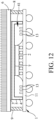
- a fifth embodiment of the semiconductor device is generally similar to the fourth embodiment, except that in the fifth embodiment, the blocking member 9 is disposed outside the heat dissipation cover 4 and the corrosion protection layer 5, and surrounds the heat dissipation cover 4 and the corrosion protection layer 5.
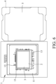
- the substrate unit 1 is not completely covered by the heat dissipation cover 4 so that a part of the substrate 11 is exposed from the heat dissipation cover 4, and the blocking member 9 is disposed between and is in contact with the anti-corrosion layer 8 and the substrate 11.
- the material of the heat conductive layer 7 is the liquid metal
- the insulating layer 12 is disposed on the substrate 11, and encapsulates the plurality of electronic components 13.
- the insulating layer 12 may not contact the corrosion protection layer 5 (see FIG. 11 ), or may abut against the corrosion protection layer 5.
- the material of the heat conductive layer 7 is the thermal grease, the thermal pad, the phase change material made of silicone oil or non-silicone oil, or the solder
- the insulating layer 12 of the semiconductor device may be dispensed with (see FIG. 12 , a variation of the fifth embodiment).
- a sixth embodiment of the semiconductor device is generally similar to the fifth embodiment, except that in the sixth embodiment, some of the electronic components 13 are located in the inner space 41 defined by the heat dissipation cover 4 and the substrate 11, and some of the electronic components 13 are located outside the heat dissipation cover 4 (e.g., located at the part of the substrate 11 that is exposed from the heat dissipation cover 4).
- the electronic components 13 may be disposed on the substrate 11 or may be embedded within the substrate 11.
- the insulating layer 12 may be disposed on the substrate 11 at a location where the electronic components 13 are disposed. When the electronic components 13 are disposed on the substrate 11, the insulating layer 12 may encapsulate the electronic components 13.
- the insulating layer 12 may be overlaid on a top of the electronic components 13, and further encapsulates the electronic components 13 within the substrate 11.
- the electronic components 13 located in the inner space 41 are disposed on (i.e., protrude from) the substrate 11, and for the electronic components 13 located outside the heat dissipation cover 4, some of them are disposed on (i.e., protrude from) the substrate 11, and some of them are embedded within the substrate 11.
- a first portion of the insulating layer 12 may encapsulate the electronic components 13 located in the inner space 41, and a second portion of the insulating layer 12 may encapsulate or be overlaid on the electronic components 13 located outside the heat dissipation cover 4 (which depends on the arrangement, i.e., protruding from or embedded within the substrate 11, of the electronic components 13).
- the material of the heat conductive layer 7 is the liquid metal
- the first portion of the insulating layer 12 is disposed on the substrate 11 and encapsulates the electronic components 13 located in the inner space 41.
- the first portion of the insulating layer 12 may not contact the corrosion protection layer 5 (see FIG.
- the material of the heat conductive layer 7 is the thermal grease, the thermal pad, the phase change material made of silicone oil or non-silicone oil, or the solder, it may be unnecessary to dispose the first portion of the insulating layer 12 on the electronic components 13 that are located in the inner space 41 (see FIG. 14 , a variation of the six embodiment).
- the blocking member 9 is disposed between the anti-corrosion layer 8 and the second portion of the insulating layer 12 and surrounds the heat dissipation cover 4 and the corrosion protection layer 5.
- the corrosion protection layer 5 and the anti-corrosion layer 8 direct contact of the liquid metal layer 3 or the heat conductive layer 7 with the heat dissipation cover 4 and the heat dissipation module 6 can be prevented.
- the formation of intermetallic compounds that are generated between the liquid metal layer 3 and the heat dissipation cover 4 can also be prevented, thus effectively maintaining the stability of the liquid metal layer 3.
- the insulating layer 12 may encapsulate the electronic components 13, thereby effectively preventing such electronic components 13 from coming into contact with any spilled liquid metal layer 3.
Landscapes
- Cooling Or The Like Of Semiconductors Or Solid State Devices (AREA)
- Structures Or Materials For Encapsulating Or Coating Semiconductor Devices Or Solid State Devices (AREA)
Applications Claiming Priority (2)
| Application Number | Priority Date | Filing Date | Title |
|---|---|---|---|
| TW112112626A TWI863204B (zh) | 2023-03-31 | 2023-03-31 | 半導體裝置 |
| EP24166301.2A EP4439656B1 (de) | 2023-03-31 | 2024-03-26 | Halbleiteranordnung |
Related Parent Applications (2)
| Application Number | Title | Priority Date | Filing Date |
|---|---|---|---|
| EP24166301.2A Division-Into EP4439656B1 (de) | 2023-03-31 | 2024-03-26 | Halbleiteranordnung |
| EP24166301.2A Division EP4439656B1 (de) | 2023-03-31 | 2024-03-26 | Halbleiteranordnung |
Publications (2)
| Publication Number | Publication Date |
|---|---|
| EP4571828A2 true EP4571828A2 (de) | 2025-06-18 |
| EP4571828A3 EP4571828A3 (de) | 2025-11-05 |
Family
ID=90675372
Family Applications (2)
| Application Number | Title | Priority Date | Filing Date |
|---|---|---|---|
| EP24166301.2A Active EP4439656B1 (de) | 2023-03-31 | 2024-03-26 | Halbleiteranordnung |
| EP25172736.8A Pending EP4571828A3 (de) | 2023-03-31 | 2024-03-26 | Halbleiteranordnung |
Family Applications Before (1)
| Application Number | Title | Priority Date | Filing Date |
|---|---|---|---|
| EP24166301.2A Active EP4439656B1 (de) | 2023-03-31 | 2024-03-26 | Halbleiteranordnung |
Country Status (5)
| Country | Link |
|---|---|
| US (1) | US20240332217A1 (de) |
| EP (2) | EP4439656B1 (de) |
| CN (1) | CN118737993A (de) |
| DK (1) | DK4439656T3 (de) |
| TW (1) | TWI863204B (de) |
Citations (1)
| Publication number | Priority date | Publication date | Assignee | Title |
|---|---|---|---|---|
| EP4057337A1 (de) | 2021-03-09 | 2022-09-14 | Morningrich Technology Co., Ltd | Elektronische vorrichtung mit wärmeableitungsstruktur |
Family Cites Families (5)
| Publication number | Priority date | Publication date | Assignee | Title |
|---|---|---|---|---|
| KR100245971B1 (ko) * | 1995-11-30 | 2000-03-02 | 포만 제프리 엘 | 중합접착제를 금속에 접착시키기 위한 접착력 촉진층을 이용하는 히트싱크어셈블리 및 그 제조방법 |
| US20110240279A1 (en) * | 2010-03-30 | 2011-10-06 | International Business Machines Corporation | Hybrid liquid metal-solder thermal interface |
| US10777483B1 (en) * | 2020-02-28 | 2020-09-15 | Arieca Inc. | Method, apparatus, and assembly for thermally connecting layers |
| TWM598743U (zh) * | 2020-04-27 | 2020-07-21 | 裕晨科技股份有限公司 | 散熱裝置 |
| US12588499B2 (en) * | 2020-06-18 | 2026-03-24 | Intel Corporation | Integrated circuit heat spreader including sealant interface material |
-
2023
- 2023-03-31 TW TW112112626A patent/TWI863204B/zh active
-
2024
- 2024-02-19 CN CN202410181802.0A patent/CN118737993A/zh active Pending
- 2024-03-26 EP EP24166301.2A patent/EP4439656B1/de active Active
- 2024-03-26 DK DK24166301.2T patent/DK4439656T3/da active
- 2024-03-26 EP EP25172736.8A patent/EP4571828A3/de active Pending
- 2024-03-29 US US18/621,401 patent/US20240332217A1/en active Pending
Patent Citations (1)
| Publication number | Priority date | Publication date | Assignee | Title |
|---|---|---|---|---|
| EP4057337A1 (de) | 2021-03-09 | 2022-09-14 | Morningrich Technology Co., Ltd | Elektronische vorrichtung mit wärmeableitungsstruktur |
Also Published As
| Publication number | Publication date |
|---|---|
| EP4439656B1 (de) | 2026-03-04 |
| EP4439656A3 (de) | 2025-01-08 |
| EP4571828A3 (de) | 2025-11-05 |
| TWI863204B (zh) | 2024-11-21 |
| TW202441735A (zh) | 2024-10-16 |
| US20240332217A1 (en) | 2024-10-03 |
| DK4439656T3 (da) | 2026-03-23 |
| CN118737993A (zh) | 2024-10-01 |
| EP4439656A2 (de) | 2024-10-02 |
Similar Documents
| Publication | Publication Date | Title |
|---|---|---|
| US11758691B2 (en) | Heat dissipation structure and electronic device adopting the same | |
| US8970029B2 (en) | Thermally enhanced heat spreader for flip chip packaging | |
| US6424033B1 (en) | Chip package with grease heat sink and method of making | |
| US4323914A (en) | Heat transfer structure for integrated circuit package | |
| US9271427B2 (en) | Flexible thermal transfer strips | |
| US8373991B2 (en) | Metal thermal interface material and thermal module and packaged microelectronic component containing the material | |
| US20110042784A1 (en) | Mechanical Barrier Element for Improved Thermal Reliability of Electronic Components | |
| US20050083655A1 (en) | Dielectric thermal stack for the cooling of high power electronics | |
| US11754343B2 (en) | Phase change heat-storing mechanisms for substrates of electronic assemblies | |
| US6246583B1 (en) | Method and apparatus for removing heat from a semiconductor device | |
| EP4057337B1 (de) | Elektronische vorrichtung mit wärmeableitungsstruktur | |
| EP1561242A2 (de) | Schottky-bauelement im chip-massstab | |
| EP4439656B1 (de) | Halbleiteranordnung | |
| CN212461665U (zh) | 一种散热盖及芯片的封装结构 | |
| US12087657B2 (en) | Semiconductor packages | |
| CN117650112A (zh) | 一种芯片封装与散热系统 | |
| JPS6142864B2 (de) | ||
| CN223786515U (zh) | 封装结构 | |
| JP2003023126A (ja) | 半導体装置 | |
| US20250233098A1 (en) | Semiconductor device | |
| CN113635648B (zh) | 一种界面导热材料的制备方法 | |
| US3462654A (en) | Electrically insulating-heat conductive mass for semiconductor wafers | |
| KR100798474B1 (ko) | 전도성 도핑층과 금속층을 갖는 반도체 칩 | |
| JP2006073744A (ja) | ヒートシンク | |
| CN119725246A (zh) | 封装结构 |
Legal Events
| Date | Code | Title | Description |
|---|---|---|---|
| PUAI | Public reference made under article 153(3) epc to a published international application that has entered the european phase |
Free format text: ORIGINAL CODE: 0009012 |
|
| STAA | Information on the status of an ep patent application or granted ep patent |
Free format text: STATUS: THE APPLICATION HAS BEEN PUBLISHED |
|
| AC | Divisional application: reference to earlier application |
Ref document number: 4439656 Country of ref document: EP Kind code of ref document: P |
|
| AK | Designated contracting states |
Kind code of ref document: A2 Designated state(s): AL AT BE BG CH CY CZ DE DK EE ES FI FR GB GR HR HU IE IS IT LI LT LU LV MC ME MK MT NL NO PL PT RO RS SE SI SK SM TR |
|
| REG | Reference to a national code |
Ref country code: DE Ref legal event code: R079 Free format text: PREVIOUS MAIN CLASS: H01L0023420000 Ipc: H01L0023373000 |
|
| PUAL | Search report despatched |
Free format text: ORIGINAL CODE: 0009013 |
|
| AK | Designated contracting states |
Kind code of ref document: A3 Designated state(s): AL AT BE BG CH CY CZ DE DK EE ES FI FR GB GR HR HU IE IS IT LI LT LU LV MC ME MK MT NL NO PL PT RO RS SE SI SK SM TR |
|
| RIC1 | Information provided on ipc code assigned before grant |
Ipc: H01L 23/373 20060101AFI20250930BHEP Ipc: H01L 23/42 20060101ALI20250930BHEP Ipc: H01L 23/31 20060101ALN20250930BHEP Ipc: H01L 23/367 20060101ALN20250930BHEP |
|
| RAP1 | Party data changed (applicant data changed or rights of an application transferred) |
Owner name: WINCHAIN MATERIAL TECHNOLOGY CO., LTD. |
|
| STAA | Information on the status of an ep patent application or granted ep patent |
Free format text: STATUS: REQUEST FOR EXAMINATION WAS MADE |