EP4571395A1 - Light output device and information generation device comprising same - Google Patents
Light output device and information generation device comprising same Download PDFInfo
- Publication number
- EP4571395A1 EP4571395A1 EP23853024.0A EP23853024A EP4571395A1 EP 4571395 A1 EP4571395 A1 EP 4571395A1 EP 23853024 A EP23853024 A EP 23853024A EP 4571395 A1 EP4571395 A1 EP 4571395A1
- Authority
- EP
- European Patent Office
- Prior art keywords
- light
- disposed
- light source
- emission pattern
- diffusion member
- Prior art date
- Legal status (The legal status is an assumption and is not a legal conclusion. Google has not performed a legal analysis and makes no representation as to the accuracy of the status listed.)
- Pending
Links
Images









Classifications
-
- G—PHYSICS
- G02—OPTICS
- G02B—OPTICAL ELEMENTS, SYSTEMS OR APPARATUS
- G02B27/00—Optical systems or apparatus not provided for by any of the groups G02B1/00 - G02B26/00, G02B30/00
- G02B27/09—Beam shaping, e.g. changing the cross-sectional area, not otherwise provided for
- G02B27/0916—Adapting the beam shape of a semiconductor light source such as a laser diode or an LED, e.g. for efficiently coupling into optical fibers
-
- G—PHYSICS
- G01—MEASURING; TESTING
- G01S—RADIO DIRECTION-FINDING; RADIO NAVIGATION; DETERMINING DISTANCE OR VELOCITY BY USE OF RADIO WAVES; LOCATING OR PRESENCE-DETECTING BY USE OF THE REFLECTION OR RERADIATION OF RADIO WAVES; ANALOGOUS ARRANGEMENTS USING OTHER WAVES
- G01S7/00—Details of systems according to groups G01S13/00, G01S15/00, G01S17/00
- G01S7/48—Details of systems according to groups G01S13/00, G01S15/00, G01S17/00 of systems according to group G01S17/00
- G01S7/481—Constructional features, e.g. arrangements of optical elements
- G01S7/4814—Constructional features, e.g. arrangements of optical elements of transmitters alone
-
- G—PHYSICS
- G01—MEASURING; TESTING
- G01B—MEASURING LENGTH, THICKNESS OR SIMILAR LINEAR DIMENSIONS; MEASURING ANGLES; MEASURING AREAS; MEASURING IRREGULARITIES OF SURFACES OR CONTOURS
- G01B11/00—Measuring arrangements characterised by the use of optical techniques
- G01B11/22—Measuring arrangements characterised by the use of optical techniques for measuring depth
-
- G—PHYSICS
- G01—MEASURING; TESTING
- G01B—MEASURING LENGTH, THICKNESS OR SIMILAR LINEAR DIMENSIONS; MEASURING ANGLES; MEASURING AREAS; MEASURING IRREGULARITIES OF SURFACES OR CONTOURS
- G01B11/00—Measuring arrangements characterised by the use of optical techniques
- G01B11/24—Measuring arrangements characterised by the use of optical techniques for measuring contours or curvatures
- G01B11/25—Measuring arrangements characterised by the use of optical techniques for measuring contours or curvatures by projecting a pattern, e.g. one or more lines, moiré fringes on the object
- G01B11/2513—Measuring arrangements characterised by the use of optical techniques for measuring contours or curvatures by projecting a pattern, e.g. one or more lines, moiré fringes on the object with several lines being projected in more than one direction, e.g. grids, patterns
-
- G—PHYSICS
- G02—OPTICS
- G02B—OPTICAL ELEMENTS, SYSTEMS OR APPARATUS
- G02B27/00—Optical systems or apparatus not provided for by any of the groups G02B1/00 - G02B26/00, G02B30/00
- G02B27/09—Beam shaping, e.g. changing the cross-sectional area, not otherwise provided for
- G02B27/0938—Using specific optical elements
- G02B27/095—Refractive optical elements
- G02B27/0955—Lenses
- G02B27/0961—Lens arrays
-
- G—PHYSICS
- G02—OPTICS
- G02B—OPTICAL ELEMENTS, SYSTEMS OR APPARATUS
- G02B27/00—Optical systems or apparatus not provided for by any of the groups G02B1/00 - G02B26/00, G02B30/00
- G02B27/18—Optical systems or apparatus not provided for by any of the groups G02B1/00 - G02B26/00, G02B30/00 for optical projection, e.g. combination of mirror and condenser and objective
-
- G—PHYSICS
- G02—OPTICS
- G02B—OPTICAL ELEMENTS, SYSTEMS OR APPARATUS
- G02B27/00—Optical systems or apparatus not provided for by any of the groups G02B1/00 - G02B26/00, G02B30/00
- G02B27/30—Collimators
-
- G—PHYSICS
- G01—MEASURING; TESTING
- G01S—RADIO DIRECTION-FINDING; RADIO NAVIGATION; DETERMINING DISTANCE OR VELOCITY BY USE OF RADIO WAVES; LOCATING OR PRESENCE-DETECTING BY USE OF THE REFLECTION OR RERADIATION OF RADIO WAVES; ANALOGOUS ARRANGEMENTS USING OTHER WAVES
- G01S17/00—Systems using the reflection or reradiation of electromagnetic waves other than radio waves, e.g. lidar systems
- G01S17/88—Lidar systems specially adapted for specific applications
- G01S17/89—Lidar systems specially adapted for specific applications for mapping or imaging
- G01S17/894—Three-dimensional [3D] imaging with simultaneous measurement of time-of-flight at a two-dimensional [2D] array of receiver pixels, e.g. time-of-flight cameras or flash lidar
Definitions
- the present invention relates to a light output device and an information generating device including the same.
- Three-dimensional (3D) content is being applied in many fields such as games, culture, education, manufacturing, and autonomous driving fields, and depth information (depth map) is required to obtain 3D content.
- Depth information is information that represents a distance in a space and represents far and near information of one point with respect to another point in a two-dimensional image.
- a method of obtaining depth information a method of radiating infrared (IR) structured light onto an object, a method using stereo cameras, and a method using a time of flight (ToF) are being used.
- IR infrared
- ToF time of flight
- a distance to an object is calculated by measuring a ToF, that is, a time taken for light to be emitted and reflected to arrive back.
- a ToF method a distance to an object is calculated by measuring a ToF, that is, a time taken for light to be emitted and reflected to arrive back.
- the greatest advantage of the ToF method is that distance information about a 3D space is quickly provided in real time.
- users can obtain accurate distance information without having to apply separate algorithms or perform hardware corrections. It is also possible to obtain accurate depth information even when measuring very close subjects or moving subjects.
- a light-emitting unit of a camera device generates and radiates an output light signal onto an object
- a light-receiving unit of the camera device receives an input light signal reflected from the object
- a depth information generating unit of the camera device generates depth information of the object using the input light signal received by the light-receiving unit.
- LiDAR light detection and ranging
- d-ToF direct-ToF
- these LiDAR cameras or d-ToF cameras require an optical system that transmits and receives a beam of a light source at the same distance at all angles.
- the technical object to be achieved by the present invention is to provide an information generating device capable of extracting depth information with high precision and resolution.
- the technical problem to be achieved by the present invention is to provide an information generating device capable of detecting the same distance at all angles.
- the technical object to be achieved by the present invention is to provide an information generating device capable of receiving an emission pattern with reduced distortion.
- a light output device includes a light source having a long axis in a first direction, a lens group disposed on the light source and configured to transform a first emission pattern output from the light source into a second emission pattern and output the second emission pattern, and a diffusion member disposed on the lens group, wherein the diffusion member includes a first surface disposed to face the light source and a second surface that is a surface opposite to the first surface, a plurality of convex patterns are disposed on the first surface, and each of the plurality of convex patterns has a long axis in a direction parallel to the first direction.
- the diffusion member may transform the second emission pattern into a third emission pattern and may output the third emission pattern.
- the second surface of the diffusion member may be a flat surface.
- Each of the plurality of convex patterns may have a semi-cylindrical shape extending in the first direction.
- the plurality of convex patterns may be disposed adjacent to each other in the first direction and a second direction perpendicular to a direction of an optical axis of the lens group.
- a plurality of convex patterns may be further disposed on the second surface of the diffusion member, and the plurality of convex patterns formed on the first surface and the plurality of convex patterns formed on the second surface may be disposed symmetrically to each other.
- Each of the plurality of convex patterns formed on the first surface and each of the plurality of convex patterns formed on the second surface may have a semi-cylindrical shape extending in the first direction.
- the light source may include a plurality of emitters disposed in an m ⁇ n matrix, and n that is the number of emitters disposed in the first direction may be greater than m that is the number of emitters disposed in a second direction perpendicular to the first direction.
- the lens group may include a first lens and a second lens sequentially disposed from the diffusion member, both surfaces of the first lens may have a convex shape, and both surfaces of the second lens may have a concave shape.
- the third emission pattern may include first and second edges that are symmetrical to each other with respect to an axis in the first direction, and third and fourth edges that are symmetrical to each other with respect to an axis in a second direction that is perpendicular to the first direction, and the first to fourth edges may have a concave shape.
- a light output device includes a light source configured to output a first emission pattern having a long axis in a first direction, a lens group disposed on the light source and configured to transform a first emission pattern into a second emission pattern and output the second emission pattern, and a diffusion member disposed on the lens group and configured to transform the second emission pattern into a third emission pattern and output the third emission pattern, wherein the third emission pattern includes first and second edges that are symmetrical to each other with respect to an axis in the first direction, and third and fourth edges that are symmetrical to each other with respect to an axis in a second direction perpendicular to the first direction, and the first to fourth edges have a concave shape.
- An optical density of the third emission pattern may decrease as a distance from a center of the third emission pattern increases in the first direction and may decrease as the distance from the center of the third emission pattern increases in the second direction.
- An optical density of the second emission pattern may decrease as a distance from a center of the second emission pattern increases in the first direction.
- a distance between the first edge and the second edge in the second direction may increase as the distance from the center of the third emission pattern increases in the first direction, and a distance between the third edge and the fourth edge in the first direction may increase as the distance from the center of the third emission pattern increases in the second direction.
- a light output device includes a light source having a long axis in a first direction, a lens group disposed on the light source, and a diffusion member disposed on the lens group, wherein the diffusion member includes a first surface disposed to face the light source and a second surface that is a surface opposite to the first surface, wherein a plurality of convex patterns may be disposed on the first surface, and each of the plurality of convex patterns may have a long axis in a direction parallel to the first direction, and the lens group includes a first lens and a second lens sequentially disposed from the diffusion member, wherein both surfaces of the first lens may have a convex shape, and both surfaces of the second lens may have a concave shape.
- the lens group may further include at least one lens disposed between the second lens and the light source, and a diameter of each of the first lens and the second lens may be less than a diameter of the at least one lens.
- An information generating device includes a light-emitting unit including the light output device, a light-receiving unit including an image sensor, and an information generating unit configured to generate depth information using an optical signal received by the light-receiving unit.
- An information generating device includes a light-emitting unit configured to output an emission pattern, a light-receiving unit configured to generate an incident pattern using the emission pattern, and an information generating unit configured to generate depth information using the incident pattern, wherein the emission pattern includes first and second edges which are symmetrical to each other with respect to an axis in a first direction, and third and fourth edges which are symmetrical to each other with respect to an axis in a second direction perpendicular to the first direction, wherein the first to fourth edges have a concave shape, and the incident pattern includes fifth and sixth edges which are symmetrical to each other with respect to the axis in the first direction, and seventh and eighth edges which are symmetrical to each other with respect to the axis in the second direction, wherein the fifth to eighth edges are flatter than the first to fourth edges.
- a distance between the first edge and the second edge in the second direction may increase as a distance from a center of the emission pattern increases in the first direction, and a distance between the third edge and the fourth edge in the first direction may increase as the distance from the center of the emission pattern increases in the second direction.
- a ratio of a distance between the first edge and the second edge in the second direction at a corner of the emission pattern to a distance between the first edge and the second edge in the second direction at the center of the emission pattern is greater than a ratio of a distance between the fifth edge and the sixth edge in the second direction at a corner of the incident pattern to a distance between the fifth edge and the sixth edge in the second direction at a center of the incident pattern
- the corner of the emission pattern may be a point at which two edges of the first to fourth edges meet
- the corner of the incident pattern may be a point at which two edges of the fifth to eighth edges meet.
- the light-emitting unit may include a plurality of emitters disposed in a shape of the emission pattern.
- the plurality of emitters may be disposed at a higher density in a central area of the light source than in an edge area of the light source.
- the plurality of emitters are disposed in an m ⁇ n matrix, and a distance between adjacent emitters may decrease in a direction toward a center of m rows and a center of n columns.
- a light output device includes a light source having a long axis in a first direction, a lens group disposed on the light source, and a diffusion member disposed on the lens group, wherein the light source includes a plurality of emitters, wherein the plurality of emitters are disposed at a higher density in a central area of the light source than in an edge area of the light source, and the diffusion member includes a first surface disposed to face the light source and a second surface that is a surface opposite to the first surface, wherein a plurality of convex patterns are disposed on the first surface, and each of the plurality of convex patterns has a long axis in a direction parallel to the first direction.
- the plurality of emitters may be disposed in an m ⁇ n matrix, and n that is the number of the plurality of emitters disposed in the first direction may be greater than m that is the number of the plurality of emitters disposed in a second direction perpendicular to the first direction.
- a light output device includes a light source, and a lens group disposed on the light source, wherein the light source includes a plurality of emitters disposed in an m ⁇ n matrix, and a distance between adjacent emitters decreases in a direction toward a center of m rows and a center of n columns.
- At least one of an imaginary line connecting a plurality of emitters disposed in the same row or an imaginary line connecting a plurality of emitters disposed in the same column may have a curve shape.
- an information generating device capable of extracting depth information with high precision and resolution and capable of detecting the same distance at all angles.
- a light source can be miniaturized, and a beam can be transmitted or received at the same distance at all angles without the use of a micro-electro mechanical system (MEMS) or the like.
- MEMS micro-electro mechanical system
- an emission pattern with reduced distortion is received, thereby enabling more accurate distance detection.
- any one element is described as being formed or disposed "on or below” another element
- such a description includes both cases in which the two elements are formed or disposed in direct contact with each other and in which one or more other elements are interposed between the two elements.
- such a description may include a case in which the one element is disposed at an upper side or a lower side with respect to another element.
- An information generating device may be an information generating device mounted in a vehicle to measure a distance between the vehicle and an object, but the present invention is not limited thereto.
- the information generating device according to the embodiment of the present invention may be a light detection and ranging (LiDAR) camera.
- the information generating device according to the embodiment of the present invention may extract depth information using a time of flight (ToF) principle.
- the information generating device may also be referred to as a depth information generating device or a camera device.
- FIG. 1 is a block diagram of an information generating device according to an embodiment of the present invention.
- FIG. 2 is a conceptual cross-sectional view of the information generating device according to an embodiment of the present invention.
- an information generating device 1000 includes a light-emitting unit 100, a light-receiving unit 200, a depth information generating unit 300, and a control unit 400.
- the light-emitting unit 100 may generate and output an output light signal in the form of a pulse wave or a continuous wave.
- the continuous wave may be in the form of a sinusoid wave or a square wave.
- the information generating device 1000 may detect a time difference or phase difference between the output light signal output from the light-emitting unit 100 and an input light signal reflected from an object and then input to the light-receiving unit 200.
- output light may be light that is output from the light-emitting unit 100 and is incident on an object
- input light may be light that is output from the light-emitting unit 100, reaches an object, and then is reflected from the object to be input to the light-receiving unit 200.
- a pattern of output light may be referred to as an emission pattern
- a pattern of input light may be referred to as an incident pattern. From a point of view of an object, the output light may be incident light, and the input light may be reflected light.
- the light-emitting unit 100 may include a light source 110, a lens group 120 disposed on the light source 110, and a diffusion member 130 disposed on the lens group 120.
- the light source 110 generates and outputs light.
- the light generated by the light source 110 may be infrared light having a wavelength of 770 nm to 3,000 nm.
- the light generated by the light source 110 may be visible light having a wavelength of 380 nm to 770 nm.
- a light-emitting diode (LED) may be used, and may have a form in which a plurality of LEDs are arranged in a certain pattern.
- the light source 110 may also include an organic light-emitting diode (OLED) or a laser diode (LD).
- the light source 110 may be a vertical cavity surface emitting laser (VCSEL).
- the VCSEL is one of laser diodes that convert an electrical signal into an optical signal and may output a wavelength of about 800 to about 1,000 nm, for example, about 850 nm or about 940 nm.
- the light source 110 is repeatedly turned on/off at certain time intervals to generate an output light signal in the form of a pulse wave or continuous wave. The certain time interval may be a frequency of the output light signal.
- the lens group 120 may collect light output from the light source 110 and may output the collected light to the outside.
- the lens group 120 may be disposed above an upper portion of the light source 110 to be spaced apart from the light source 110.
- the upper portion of the light source 110 may be a side through which light is output from the light source 110.
- the lens group 120 may include at least one lens.
- each of the lenses may be arranged with respect to a central axis to form an optical system.
- the central axis may be identical to an optical axis of the optical system.
- the diffusion member 130 may receive light output from the light source 110 and the lens group 120 and then may output the received light by refracting or diffracting the light.
- the light-receiving unit 200 may receive an optical signal reflected from an object.
- the received optical signal may be an optical signal output by the light-emitting unit 100 and reflected from an object.
- the light-receiving unit 200 may include an image sensor 210, a filter 220 disposed on the image sensor 210, and a lens group 230 disposed on the filter 220.
- a light signal reflected from an object may pass through the lens group 230.
- An optical axis of the lens group 230 may be aligned with an optical axis of the image sensor 210.
- the filter 220 may be disposed between the lens group 230 and the image sensor 210.
- the filter 220 may be disposed on an optical path between an object and the image sensor 210.
- the filter 220 may filter light having a certain wavelength range.
- the filter 220 may transmit light in a specific wavelength band.
- the filter 220 may transmit light with a specific wavelength.
- the filter 220 may transmit light in an infrared band and may block light outside the infrared band.
- the image sensor 210 may sense light.
- the image sensor 210 may receive an optical signal.
- the image sensor 210 may detect an optical signal and may output an electrical signal.
- the image sensor 210 may detect light with a wavelength corresponding to a wavelength of light output by the light source 110.
- the image sensor 210 may detect light in an infrared band.
- the image sensor 210 may have a structure in which a plurality of pixels are arranged in a grid form.
- the image sensor 210 may be a complementary metal oxide semiconductor (CMOS) image sensor or may be a charge coupled device (CCD) image sensor.
- CMOS complementary metal oxide semiconductor
- CCD charge coupled device
- the image sensor 210 may include a ToF sensor that receives infrared (IR) light reflected from an object and measures a distance using a time difference or phase difference.
- IR infrared
- the light-receiving unit 200 and the light-emitting unit 100 may be disposed side by side.
- the light-receiving unit 200 may be disposed next to the light-emitting unit 100.
- the light-receiving unit 200 may be disposed in the same direction as the light-emitting unit 100.
- the depth information generating unit 300 may generate depth information of an object using an input light signal input to the light-receiving unit 200. For example, the depth information generating unit 300 may calculate depth information of an object using a flight time taken for an output light signal output from the light-emitting unit 100 to be reflected from an object and then input to the light-receiving unit 200. For example, the depth information generating unit 300 may calculate a time difference between an output light signal and an input light signal using an electric signal received by the image sensor 210 and may calculate a distance between an object and the information generating device 1000 using the calculated time difference. For example, the depth information generating unit 300 may calculate a phase difference between an output light signal and an input light signal using an electrical signal received from a sensor and may calculate a distance between an object and the information generating device 1000 using the calculated phase difference.
- the control unit 400 controls the driving of the light-emitting unit 100, the light-receiving unit 200, and the depth information generating unit 300.
- the depth information generating unit 300 and the control unit 400 may be implemented in the form of a printed circuit board (PCB).
- the depth information generating unit 300 and the control unit 400 may be implemented in the form of different configurations.
- the control unit 400 may be included in a terminal or vehicle in which the information generating device 1000 according to the embodiment of the present invention is disposed.
- control unit 400 may be implemented in the form of an application processor (AP) of a smartphone equipped with the information generating device 1000 according to the embodiment of the present invention or may be implemented in the form of an electronic control unit (ECU) of a vehicle equipped with the information generating device 1000 according to the embodiment of the present invention.
- AP application processor
- ECU electronice control unit
- a LiDAR camera aims to detect the same distance at all angles.
- the lens group 230 of the light-receiving unit 200 may include an f-theta optical system or an f-sine theta optical system.
- FIG. 3 is a diagram for describing a principle of an f-theta optical system.
- an object height OH may be expressed as in Equation 1
- an image height IH may be expressed as in Equation 2.
- the object height OH may refer to a position of an object, that is, the position of the object in a horizontal direction perpendicular to an optical axis from the optical axis
- the image height IH may refer to a position on the image sensor in the horizontal direction perpendicular to the optical axis from the optical axis and may refer to pixel coordinates on the image sensor.
- a distance D may be a certain distance to an object from the information generating device (for example, the lens group 230 in the information generating device).
- a focal length f may correspond to a distance from the lens group 230 to the image sensor 210.
- An incident angle ⁇ may correspond to an angle of light incident on the lens group 230 from an object.
- the image height IH reaching the image sensor 210 may not be proportional to the object height OH. In this way, it can be seen that, when the f-theta optical system is used, it is possible to detect the same distance at all angles.
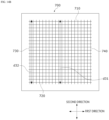
- FIGS. 4A and 4B illustrate a shape of an incident pattern when the lens group of the light-receiving unit includes the f-theta optical system.
- the reflection pattern may have an incident pattern with a transformed shape as shown in FIG. 4B .
- the light-receiving unit should include the f-theta optical system to detect the same distance at all angles, but an incident pattern incident on the image sensor 210 of the light-receiving unit 200 may be distorted due to the f-theta optical system, which may lower the accuracy of depth information.
- it is intended to compensate for the distortion of an incident pattern incident on the image sensor 210 of the light-receiving unit 200 using an emission pattern output from the light-emitting unit 100.
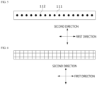
- FIG. 5 is a top view illustrating an arrangement shape of a light source included in a light-emitting unit of a camera device according to one embodiment of the present invention.
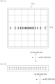
- FIG. 6 illustrates a first emission pattern output from the light source shown in FIG. 5 .
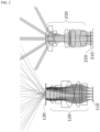
- FIG. 7 is a cross-sectional view of a lens group included in a light-emitting unit according to one embodiment of the present invention.
- FIG. 8 illustrates a second emission pattern output from the lens group of FIG. 7 .
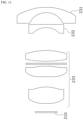
- FIGS. 9A to 9C are perspective views of a diffusion member included in the light-emitting unit according to one embodiment of the present invention.
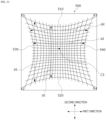
- FIG. 10 illustrates a third emission pattern output from the diffusion member of FIGS. 9A to 9C .
- a light source 110 may include a plurality of light-emitting elements 112.
- the light source 110 may be implemented in the form of an array in which the plurality of light-emitting elements 112 are disposed on a substrate 111 according to a certain rule.
- the plurality of light-emitting elements 112 may be VCSELs. That is, the light source 110 may include a plurality of emitters 112 disposed in an m ⁇ n matrix, and n that is the number of emitters 112 disposed in a first direction may be greater than m that is the number of emitters 112 disposed in a second direction perpendicular to the first direction.
- n may be an integer of 2 or more
- m may be an integer of 1 or more. Accordingly, the light source 110 may have a long axis in the first direction.
- the first emission pattern output from the light source 110 may correspond to an arrangement shape of the light source 110 and may have a long axis in the first direction.
- the first emission pattern is exemplified as a line pattern in which a line in the first direction intersects a line in the second direction, but the present invention is not limited thereto.
- the first emission pattern may be a dot pattern or a surface pattern.
- the dot pattern may be an array form of spots spaced from each other at certain intervals in a certain area.
- the surface pattern may be in a form in which light is uniformly spread in a certain area and may be used interchangeably with a flood lighting pattern, a surface light source pattern, or the like.
- uniformity may mean that light is spread continuously in a space.
- both the first direction and the second direction may be directions perpendicular to a direction of an optical axis.
- a lens group 120 may include a plurality of lenses disposed on the light source 110 and sequentially disposed in a direction from a diffusion member 130 toward the light source 110.
- the lens group 120 may include five lenses sequentially disposed in the direction from the diffusion member 130 toward the light source 110.
- the lens group 120 may be referred to as a collimator because the lens group 120 collects light output from the light source 110 to output the collected light.
- the lens group 120 may include a first lens 121 that is positioned closest to the diffusion member 130 and has both surfaces with a convex shape, and a second lens 122 that is positioned closest to the first lens 121 and has both surfaces with a concave shape.
- the lens group 120 may further include at least one lens 123 positioned between the second lens 122 and the light source 110. In this case, a diameter or effective diameter of each of the first lens 121 and the second lens 122 may be less than a diameter or effective diameter of the at least one lens 123.
- the first lens 121 and the second lens 122 serve to transform the first emission pattern output from the light source 110 into the second emission pattern, and at least one lens 123 serves to correct a chromatic aberration.
- the first emission pattern may be distorted by the lens group 120 and thus may be output as the second emission pattern.
- the first emission pattern shown in FIG. 6 has a long axis in the first direction and has an overall uniform line pattern interval.
- the second emission pattern shown in FIG. 8 has a long axis in the first direction, a line pattern interval becomes narrower in a direction toward a center of the second emission pattern, and a line pattern interval becomes wider in a direction away from the center of the second emission pattern.
- the line pattern interval may be an optical density.
- an optical density of the second emission pattern having the long axis in the first direction may decrease as a distance from the center of the second emission pattern increases in the first direction.
- an optical density of the second emission pattern having the long axis in the first direction may decrease as the distance from the center of the second emission pattern increases in the second direction.
- the second emission pattern is exemplified as a line pattern, but the present invention is not limited thereto.
- the second emission pattern may be a dot pattern or a surface pattern.
- the diffusion member 130 may be disposed on the lens group 120.
- the diffusion member 130 may also be referred to as a diffuser.
- the diffusion member 130 includes a first surface 130A disposed to face the light source 110 and a second surface 130B that is a surface opposite to the first surface 130A.
- FIG. 9A illustrates the first surface 130A facing downward
- FIG. 9B illustrates the first surface 130 facing upward by rotating FIG. 9A by 180 degrees
- FIG. 9C is a plan view of the first surface 130A.
- a plurality of convex patterns 131 may be disposed on the first surface 130A of the diffusion member 130, the second surface 130B of the diffusion member 130 may be a flat surface, and each of the plurality of convex patterns 131 may extend to have a long axis in a direction parallel to the first direction. More specifically, according to an embodiment of the present invention, each of the plurality of convex patterns 131 may have a semi-cylindrical shape extending in the first direction, and the plurality of convex patterns 131 may be disposed adjacent to each other in the second direction perpendicular to the first direction.
- the second emission pattern may be transformed by the diffusion member 130 according to the embodiment of the present invention and then may be output as a third emission pattern 500.
- the second emission pattern may be diffused in the second direction by the diffusion member 130 according to the embodiment of the present invention and then may be output as the third emission pattern 500.
- the third emission pattern 500 may include first and second edges 510 and 520 that are symmetrical to each other with respect to an axis in the first direction, and third and fourth edges 530 and 540 that are symmetrical to each other with respect to an axis in the second direction perpendicular to the first direction, and the first to fourth edges 510, 520, 530, and 540 may have a concave shape.
- the third emission pattern 500 is exemplified as a line pattern, but the present invention is not limited thereto.
- the third emission pattern 500 may be a dot pattern or a surface pattern.
- an edge of a light pattern may be a periphery of a light distribution area having an optical density that is significant for generating depth information.
- the concave shape of the first edge 510 may mean that the first edge 510 has a shape gently curved toward a center C3 of the third emission pattern 500.
- the fact that the second to fourth edges 520, 530, and 540 have the concave shape may mean that the second to fourth edges 520, 530, and 540 have a shape gently curved toward the center C3 of the third emission pattern 500.
- a distance d1 between the first edge 510 and the second edge 320 in the second direction may increase as a distance from the center C3 of the third emission pattern 500 increases in the first direction
- a distance d2 between the third edge 530 and the fourth edge 540 in the first direction may increase as a distance from the center C3 of the third emission pattern 500 increases in the second direction.
- an optical density of the third emission pattern 500 may decrease as the distance from the center C3 of the third emission pattern 500 increases in the first direction and may decrease as the distance from the center C3 of the third emission pattern 500 increases in the second direction.
- An area with the highest optical density in the third emission pattern 500 may be the center C3 of the third emission pattern 500, and areas with the lowest optical density in the third emission pattern 500 may be a point E1 at which the first and third edges 510 and 530 meet, a point E2 at which the second and third edges 320 and 330 meet, a point E3 at which the first and fourth edges 310 and 340 meet, and a point E4 at which the second and fourth edges 320 and 340 meet.
- the third emission pattern 500 output from the diffusion member 130 may be reflected from an object and then may be incident on a light-receiving unit 200.
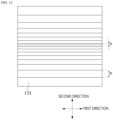
- FIGS. 11A , 11B , and 12 illustrate a diffusion member according to another embodiment of the present invention.
- a plurality of convex patterns 132 may also be disposed on a second surface 130B which is a surface opposite to a first surface 130A disposed to face a light source 110 among both surfaces of a diffusion member 130. That is, according to another embodiment of the present invention, the plurality of convex patterns 132 may also be disposed on the second surface 130B of the diffusion member 130, and each of the plurality of convex patterns 132 may extend to have a long axis in a direction parallel to a first direction.
- each of the plurality of convex patterns 132 may have a semi-cylindrical shape extending in the first direction, and the plurality of convex patterns 132 may be disposed adjacent to each other in a second direction perpendicular to the first direction.
- a plurality of convex patterns 131 formed on the first surface 130A and the plurality of convex patterns 132 formed on the second surface 130B may be disposed symmetrically to each other.
- each of the plurality of convex patterns 131 formed on the first surface 130A and each of the plurality of convex patterns 132 formed on the second surface 130B may form one cylindrical shape extending in the first direction.
- the plurality of convex patterns 131 may have different pitches P.
- each of the plurality of convex patterns 131 may have a semi-cylindrical shape extending in the first direction
- the plurality of convex patterns 131 may be disposed adjacent to each other in the second direction perpendicular to the first direction
- diameters of the semi-cylindrical shapes of the plurality of convex patterns 131, that is, distances in the second direction may be designed to be different.
- a diameter of the semi-cylindrical shape of the plurality of convex patterns 131 is illustrated as increasing from a central area of the diffusion member 130 to an edge area, but the present invention is not limited thereto.
- the diameter of the semi-cylindrical shape of the plurality of convex patterns 131 may decrease from the central area of the diffusion member 130 to the edge area.
- the diameter of the semi-cylindrical shape of the plurality of convex patterns 131 may increase and then decrease again from the central area of the diffusion member 130 to the edge area.
- the diameter of the semi-cylindrical shape of the plurality of convex patterns 131 may be randomly designed without any regularity.
- the energy of output light may be dispersed, which may increase the safety for the user's eyes and may also prevent degradation in homogeneity due to interference.
- pitches of the plurality of convex patterns 131 formed on the first surface 130A of the diffusion member 130 are mainly described, the present invention is not limited thereto, and pitches of the plurality of convex patterns 132 formed on the second surface 130B of the diffusion member 130 may be designed to be symmetrical to the pitches of the plurality of convex patterns 131 formed on the first surface 130A of the diffusion member 130.
- a LiDAR camera is directed to detecting the same distance at all angles.
- a lens group 230 of a light-receiving unit 200 may include an f-theta optical system or an f-sine theta optical system.
- FIG. 13 is a cross-sectional view of a lens group of a light-receiving unit according to one embodiment of the present invention.
- a lens group 230 includes a plurality of lenses sequentially disposed from an object (subject) to an upper side (image sensor 210 side).
- the lens group 230 may include a first lens 231 which is disposed closest to the object and of which a surface facing the object has a convex shape and an upper surface has a concave shape, and a second lens 232 which is disposed closest to the first lens 231 and of which a surface facing the object has a flat shape and an upper surface has a concave shape.
- the lens group 230 may further include at least one lens 233 disposed between the second lens 232 and the image sensor 210.
- the first lens 231 may have the largest diameter or effective diameter among the plurality of lenses included in the lens group 230
- the second lens 232 may have the smallest diameter or effective diameter among the plurality of lenses included in the lens group 230.
- a distance between the second lens 232 and a lens positioned closest to the object among at least one lens 233 may be the longest among distances between the lenses included in the lens group 230.
- the first lens 231 and the second lens 232 serve to transform a third emission pattern reflected from an object into an incident pattern incident on the image sensor 210, and at least one lens 233 serves to correct a chromatic aberration.
- FIGS. 14A and 14B illustrate a transformation of a light pattern by a lens group of a light-receiving unit according to an embodiment of the present invention.
- FIG. 14A illustrates a shape of a light pattern that is incident on a lens group 230 of a light-receiving unit 200 after a third emission pattern 500 output from a light-emitting unit 100 is reflected from an object as described above.
- FIG. 14B illustrates a shape of a light pattern incident on an image sensor after the light pattern of FIG. 14A passes through the lens group of the light-receiving unit according to the embodiment of the present invention.
- a light pattern 600 incident on the lens group 230 of the light-receiving unit 200 may have the same shape as the third emission pattern 500 and may include first and second edges 610 and 620 that are symmetrical to each other with respect to an axis in a first direction, and third and fourth edges 630 and 640 that are symmetrical to each other with respect to an axis in a second direction perpendicular to the first direction.
- the first to fourth edges 610, 620, 630, and 640 may have a concave shape.
- an incident pattern 700 that is transformed by the lens group 230 of the light-receiving unit 200 and then is incident on the image sensor 210 includes fifth and sixth edges 710 and 720 that are symmetrical to each other with respect to the axis in the first direction, and seventh and eighth edges 730 and 740 that are symmetrical to each other with respect to the axis in the second direction.
- the fifth to eighth edges 710, 720, 730, and 740 are flatter than the first to fourth edges 610, 620, 630, and 630.
- a distance between the first edge 610 and the second edge 620 in the second direction in the light pattern 600 increases as a distance from a center of the light pattern 600 increases in the first direction
- a distance between the third edge 630 and the fourth edge 640 in the first direction increases as the distance from the center of the light pattern 600 increases in the second direction
- a ratio d12/d11 of a distance d12 between the first edge 610 and the second edge 620 in the second direction at an edge of the light pattern to a distance d11 between the first edge 610 and the second edge 620 in the second direction at the center of the light pattern 600 is greater than a ratio d32/d31 of a distance d32 between the fifth edge 710 and the sixth edge 720 in the second direction at an edge of the incident pattern 700 to a distance d31 between the fifth edge 710 and the sixth edge 720 in the second direction at the center of the incident pattern 700.
- a ratio of a distance between the third edge 630 and the fourth edge 640 in the first direction at the edge of the light pattern 600 to a distance between the third edge 630 and the fourth edge 640 in the first direction at the center of the light pattern 600 may be greater than a ratio of a distance between the seventh edge 730 and the eighth edge 740 in the first direction at the edge of the incident pattern 700 to a distance between the seventh edge 730 and the eighth edge 740 in the first direction at the center of the incident pattern 700.
- the edge of the light pattern 600 may be a point at which two edges of the first to fourth edges meet
- the edge of the incident pattern 700 may be a point at which two edges of the fifth to eighth edges meet.
- the incident pattern 700 may have a grid shape corresponding to a pixel array of the image sensor 210, and depth information may be generated with high accuracy without distortion while the same distance at all angles is detected.
- the light-emitting unit 100 may also control an emission pattern output from the light-emitting unit 100 using an arrangement shape of the light source 110.
- FIGS. 15A and 15B illustrate an arrangement shape of a light source according to another embodiment of the present invention.
- a light source 110 includes a plurality of emitters 112 and may be disposed to have a long axis in a first direction.
- the plurality of emitters 112 may be disposed to have a higher density in a central area of the light source 110 than in an edge area of the light source 110.
- the plurality of emitters 112 are disposed in an m ⁇ n matrix, and n that is the number of emitters 112 disposed in the first direction may be greater than m that is the number of emitters 112 disposed in a second direction perpendicular to the first direction.
- the number m of emitters 112 disposed in the second direction may be greater than 2.
- a distance between the plurality of emitters 112 disposed in the first direction may increase as a distance from a center of the light source 110 increases, and a distance between the plurality of emitters 112 disposed in the second direction may increase as the distance from the center of the light source 110 increases.
- an emission pattern output from the light source 110 may be as shown in FIG. 15B and may be the same as the second emission pattern output from the lens group 120 shown in FIG. 8 .
- the light-emitting unit 100 may include a general lens group. That is, the light-emitting unit 100 may include a lens group that does not cause distortion, rather than the lens group 120 shown in FIG. 7 .
- the light-emitting unit 100 may include the diffusion member 130 shown in FIGS. 9A to 9C . Even in this case, the diffusion member 130 may be formed to be elongated in the first direction. That is, a plurality of convex patterns are disposed on the diffusion member 130, and each of the plurality of convex patterns may extend to have a long axis in a direction parallel to the first direction.
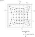
- FIGS. 16A and 16B illustrate an arrangement shape of a light source according to still another embodiment of the present invention.
- a light source 110 may include a plurality of emitters 112, and the plurality of emitters 112 may be disposed in an m ⁇ n matrix and may be disposed such that a distance between adjacent emitters 112 decreases in a direction toward a center of m rows and a center of n columns.
- An imaginary line connecting a plurality of emitters disposed in the same row or an imaginary line connecting a plurality of emitters disposed in the same column may have a curve shape.
- n that is the number of emitters 112 disposed in the first direction may be equal to m that is the number m of emitters 112 disposed in a second direction perpendicular to the first direction, but the present invention is not limited thereto.
- imaginary lines connecting the plurality of emitters 112 disposed at the outermost edge may include first and second imaginary lines VL1 and VL2 that are symmetrical to each other with respect to an axis in the first direction, and third and fourth imaginary lines VL3 and VL4 that are symmetrical to each other with respect to an axis in the second direction.
- the first to fourth imaginary lines VL1 to VL4 may have a concave shape.
- the fact that the first imaginary line VL1 has the concave shape may mean that the first imaginary line VL1 has a shape gently curved toward a center of the light source 110.
- the fact that the second to fourth imaginary lines VL2 to VL4 have the concave shape may mean that the second to fourth imaginary lines VL2 to VL4 have a shape gently curved toward the center of the light source 110.
- a distance between the first imaginary line VL1 and the second imaginary line VL2 in the second direction may increase as a distance from the center of the light source 110 increases in the first direction
- a distance between the third imaginary lines VL3 and the fourth imaginary line VL4 in the first direction may increase as the distance from the center of the light source 110 increases in the second direction.
- a distance between the plurality of emitters 112 disposed in the first direction to pass through the center of the light source 110 may be equal to a distance between the plurality of emitters 112 disposed in the second direction to pass through the center of the light source 110.
- the distance between the plurality of emitters 112 disposed in the first direction to pass through the center of the light source 110 may not be equal to the distance between the plurality of emitters 112 disposed in the second direction to pass through the center of the light source 110.
- a distance between the plurality of emitters 112 may increase as the distance from the center of the light source 110 increases.
- an emission pattern output from the light source 110 may be as shown in FIG. 16B and may be the same as the third emission pattern 500 output from the diffusion member 130 shown in FIG. 10 .
- the light-emitting unit 100 may include a general lens group. That is, the light-emitting unit 100 may include a lens group that does not cause distortion, rather than the lens group 120 shown in FIG. 7 .
- the light-emitting unit 100 may not include the diffusion member 130 shown in FIGS. 9A to 9C . That is, the light-emitting unit 100 may radiate a light signal output from the lens group 120 onto an object.
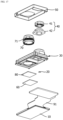
- FIG. 17 is an exploded view of a camera module according to an embodiment of the present invention.
- the camera module may include a light-emitting unit and a light-receiving unit.
- components such as a substrate 10, a holder 30, and a shield can 50 are integrally formed and commonly used for the light-emitting unit and the light-receiving unit, the components may be difficult to distinguish between the light-emitting unit and the light-receiving unit.
- each of the components may be understood as a component of each of the light-emitting unit and the light-receiving unit.
- the common components such as the substrate 10, the holder 30, and the shield can 50 may be separately provided to each of the light-emitting unit and the light-receiving unit.
- the light-emitting unit may include the substrate 10, a light source 20, the holder 30, a diffusion member 41, a diffuser ring 42, and the shield can 50.
- the light-receiving unit may include the substrate 10, a sensor 60, a filter 80, a holder 30, a lens 70, a barrel 71, and the shield can 50.
- the substrate 10 may include a PCB.
- the substrate 10 may be connected to a connector through a flexible PCB (FPCB) 91.
- the substrate 10 and the FPCB 91 may be formed as rigid flexible PCBs (RFPCBs).
- a light source 20 and the sensor 60 may be disposed on the substrate 10.
- the substrate 10 may be disposed below the holder 30.
- the substrate 10 may include terminals.
- the terminal of the substrate 10 may be connected to a coupling portion of the shield can 50.
- the terminals of the substrate 10 may include a plurality of terminals.
- the terminals of the substrate 10 may include two terminals.
- the light source 20 may be disposed on the substrate 10.
- the light source 20 may be disposed in contact with the substrate 10.
- the light source 20 may be disposed above the substrate 10.
- the light source 20 may be disposed on the substrate 10.
- the light source 20 may correspond to the light source 110 described above.
- the holder 30 may be disposed on the substrate 10.
- the holder 30 may be disposed in contact with the substrate 10.
- the holder 30 may be disposed above the substrate 10.
- the holder 30 may be disposed on the substrate 10.
- the holder 30 may be fixed to the substrate 10 through an adhesive.
- the holder 30 may accommodate the light source 20, a diffuser module 40, the sensor 60, and the filter 80 therein.
- the holder 30 may be a plastic injection molded product.
- the holder 30 may be formed through injection molding.
- the diffuser module 40 may include the diffusion member 41 and the diffuser ring 42.
- the diffuser module 40 may be integrally formed as in the modified example, but in the present embodiment, the diffuser module 40 may be manufactured to be separated into the diffusion member 41 and the diffuser ring 42 to increase moldability during injection molding.
- the diffusion member 41 and the diffuser ring 42 may be separated from each other.
- the diffusion member 41 may be a diffuser lens.
- the diffusion member 41 may correspond to the diffusion member 130 described above.
- the diffusion member 41 may be disposed in the holder 30.
- the diffusion member 41 may be coupled to the holder 30.
- the diffusion member 41 may be fixed to the holder 30.
- the diffusion member 41 may be disposed on an optical path of light emitted from the light source 20.
- the diffusion member 41 may be disposed on the light source 20.
- the diffusion member 41 may be disposed above the light source 20.
- the diffusion member 41 may be a plastic injection molded product.
- the diffusion member 41 may be formed through plastic injection molding.
- a height of an upper end of the diffusion member 41 may correspond to a height of an upper end of the lens 70.
- the diffusion member 41 may be inserted in an upward direction of a vertical direction and coupled to the holder 30.
- the upward direction may be a direction from a lower portion of the holder 30 toward an upper portion of the holder 30.
- a portion of the diffusion member 41 may overlap the holder 30 in the upward direction.
- the diffuser ring 42 may be disposed in the holder 30.
- the diffuser ring 42 may be fixed to the holder 30.
- the diffuser ring 42 may be coupled to the holder 30.
- the diffuser ring 42 may be disposed below the diffusion member 41.
- the diffuser ring 42 may support the diffusion member 41.
- the diffuser ring 42 may be in contact with the diffusion member 41.
- the diffuser ring 42 may be a plastic injection molded product.
- the diffuser ring 42 may be formed through plastic injection molding.
- the shield can 50 may cover a body of the holder 30.
- the shield can 50 may include a cover.
- the shield can 50 may include a cover can.
- the shield can 50 may be a nonmagnetic body.
- the shield can 50 may be formed of a metal material.
- the shield can 50 may be formed of a metal plate.
- the shield can 50 may be electrically connected to the substrate 10.
- the shield can 50 may be connected to the substrate 10 through solder balls. Thus, the shield can 50 may be grounded.
- the shield can 50 may block electromagnetic interference (EMI) noise.
- the shield can 500 may be referred to as "EMI shield can."
- EMI shield can since a high voltage is used inside an optical device, EMI noise may increase, and the shield can 50 may block the EMI noise.
- the sensor 60 may be disposed on the substrate 10.
- the sensor 60 may be disposed at the other side of a partition wall of the holder 30 on the substrate 10. That is, the sensor 60 may be disposed at a side opposite to the light source 20 with respect to the partition wall of the holder 30.
- the sensor 60 may detect infrared rays.
- the sensor 60 may detect light with a specific wavelength among infrared rays.
- the sensor 60 may detect light passing through the filter 80.
- the sensor 60 may detect light in a wavelength band of the light source 20.
- the sensor 60 may detect light emitted from the light source 20 and reflected on a subject, thereby sensing three-dimensional (3D) image information of the subject.
- An effective sensing area of the sensor 60 is disposed to correspond to the diffusion member 41, but the sensor 60 may be disposed to be entirely biased toward the partition wall.
- a circuit pattern or the like of the sensor 60 may be disposed in a portion of the sensor 60 that is biased toward the partition wall.
- the lens 70 may be fixed in the barrel 71.
- the lens 70 may be a plastic injection molded product.
- the lens 70 may be formed through plastic injection molding.
- the lens 70 may include a plurality of lenses.
- the filter 80 may be disposed between the lens 70 and the sensor 60.
- the filter 80 may be a band pass filter that transmits light in a specific wavelength band.
- the filter 80 may transmit infrared light.
- the filter 80 may transmit light with a specific wavelength in infrared light.
- the filter 80 may transmit light in a wavelength band of light emitted by the light source 20.
- the filter 80 may block visible light.
- the filter 80 may be coupled to the holder 30.
- a groove with a size corresponding to the filter 80 may be formed in the holder 30, and the filter 80 may be inserted into the groove and fixed through an adhesive.
- An adhesive injection groove for injecting an adhesive between the filter 80 and the holder 30 may be formed in the groove of the holder 30.
- the filter 80 may be positioned at a lower level than the diffuser ring 42.
- a camera device may be a camera device that extracts depth information using a structured light method. That is, the camera device according to the embodiment of the present invention may use structured light having a certain pattern as an output light signal and may generate depth information using the disparity of the structured light.
Landscapes
- Physics & Mathematics (AREA)
- General Physics & Mathematics (AREA)
- Engineering & Computer Science (AREA)
- Optics & Photonics (AREA)
- Computer Networks & Wireless Communication (AREA)
- Radar, Positioning & Navigation (AREA)
- Remote Sensing (AREA)
- Electromagnetism (AREA)
- Computer Vision & Pattern Recognition (AREA)
- Lenses (AREA)
- Measurement Of Optical Distance (AREA)
- Optical Radar Systems And Details Thereof (AREA)
Abstract
A light output device according to an embodiment of the present invention comprises: a light source having a long axis in a first direction; a lens group which is arranged on the light source, and which deforms a first light-emitting pattern that is output from the light source into a second light-emitting pattern and outputs same; and a diffusion member arranged on the lens group, wherein: the diffusion member includes a first surface arranged to face the light source, and a second surface that is opposite to the first surface; a plurality of convex patterns are arranged on the first surface; and each of the plurality of convex patterns has a long axis in the direction parallel to the first direction.
Description
- The present invention relates to a light output device and an information generating device including the same.
- Three-dimensional (3D) content is being applied in many fields such as games, culture, education, manufacturing, and autonomous driving fields, and depth information (depth map) is required to obtain 3D content. Depth information is information that represents a distance in a space and represents far and near information of one point with respect to another point in a two-dimensional image. As a method of obtaining depth information, a method of radiating infrared (IR) structured light onto an object, a method using stereo cameras, and a method using a time of flight (ToF) are being used.
- According to a ToF method, a distance to an object is calculated by measuring a ToF, that is, a time taken for light to be emitted and reflected to arrive back. The greatest advantage of the ToF method is that distance information about a 3D space is quickly provided in real time. In addition, users can obtain accurate distance information without having to apply separate algorithms or perform hardware corrections. It is also possible to obtain accurate depth information even when measuring very close subjects or moving subjects.
- Meanwhile, in order to obtain depth information, a light-emitting unit of a camera device generates and radiates an output light signal onto an object, a light-receiving unit of the camera device receives an input light signal reflected from the object, and a depth information generating unit of the camera device generates depth information of the object using the input light signal received by the light-receiving unit.
- Typically, light detection and ranging (LiDAR) cameras or direct-ToF (d-ToF) cameras aim to detect the same distance at all angles. To this end, these LiDAR cameras or d-ToF cameras require an optical system that transmits and receives a beam of a light source at the same distance at all angles.
- The technical object to be achieved by the present invention is to provide an information generating device capable of extracting depth information with high precision and resolution.
- The technical problem to be achieved by the present invention is to provide an information generating device capable of detecting the same distance at all angles.
- The technical object to be achieved by the present invention is to provide an information generating device capable of receiving an emission pattern with reduced distortion.
- A light output device according to an embodiment of the present invention includes a light source having a long axis in a first direction, a lens group disposed on the light source and configured to transform a first emission pattern output from the light source into a second emission pattern and output the second emission pattern, and a diffusion member disposed on the lens group, wherein the diffusion member includes a first surface disposed to face the light source and a second surface that is a surface opposite to the first surface, a plurality of convex patterns are disposed on the first surface, and each of the plurality of convex patterns has a long axis in a direction parallel to the first direction.
- The diffusion member may transform the second emission pattern into a third emission pattern and may output the third emission pattern.
- The second surface of the diffusion member may be a flat surface.
- Each of the plurality of convex patterns may have a semi-cylindrical shape extending in the first direction.
- The plurality of convex patterns may be disposed adjacent to each other in the first direction and a second direction perpendicular to a direction of an optical axis of the lens group.
- A plurality of convex patterns may be further disposed on the second surface of the diffusion member, and the plurality of convex patterns formed on the first surface and the plurality of convex patterns formed on the second surface may be disposed symmetrically to each other.
- Each of the plurality of convex patterns formed on the first surface and each of the plurality of convex patterns formed on the second surface may have a semi-cylindrical shape extending in the first direction.
- The light source may include a plurality of emitters disposed in an m×n matrix, and n that is the number of emitters disposed in the first direction may be greater than m that is the number of emitters disposed in a second direction perpendicular to the first direction.
- The lens group may include a first lens and a second lens sequentially disposed from the diffusion member, both surfaces of the first lens may have a convex shape, and both surfaces of the second lens may have a concave shape.
- The third emission pattern may include first and second edges that are symmetrical to each other with respect to an axis in the first direction, and third and fourth edges that are symmetrical to each other with respect to an axis in a second direction that is perpendicular to the first direction, and the first to fourth edges may have a concave shape.
- A light output device according to another embodiment of the present invention includes a light source configured to output a first emission pattern having a long axis in a first direction, a lens group disposed on the light source and configured to transform a first emission pattern into a second emission pattern and output the second emission pattern, and a diffusion member disposed on the lens group and configured to transform the second emission pattern into a third emission pattern and output the third emission pattern, wherein the third emission pattern includes first and second edges that are symmetrical to each other with respect to an axis in the first direction, and third and fourth edges that are symmetrical to each other with respect to an axis in a second direction perpendicular to the first direction, and the first to fourth edges have a concave shape.
- An optical density of the third emission pattern may decrease as a distance from a center of the third emission pattern increases in the first direction and may decrease as the distance from the center of the third emission pattern increases in the second direction.
- An optical density of the second emission pattern may decrease as a distance from a center of the second emission pattern increases in the first direction.
- A distance between the first edge and the second edge in the second direction may increase as the distance from the center of the third emission pattern increases in the first direction, and a distance between the third edge and the fourth edge in the first direction may increase as the distance from the center of the third emission pattern increases in the second direction.
- A light output device according to still another embodiment of the present invention includes a light source having a long axis in a first direction, a lens group disposed on the light source, and a diffusion member disposed on the lens group, wherein the diffusion member includes a first surface disposed to face the light source and a second surface that is a surface opposite to the first surface, wherein a plurality of convex patterns may be disposed on the first surface, and each of the plurality of convex patterns may have a long axis in a direction parallel to the first direction, and the lens group includes a first lens and a second lens sequentially disposed from the diffusion member, wherein both surfaces of the first lens may have a convex shape, and both surfaces of the second lens may have a concave shape.
- The lens group may further include at least one lens disposed between the second lens and the light source, and a diameter of each of the first lens and the second lens may be less than a diameter of the at least one lens.
- An information generating device according to an embodiment of the present invention includes a light-emitting unit including the light output device, a light-receiving unit including an image sensor, and an information generating unit configured to generate depth information using an optical signal received by the light-receiving unit.
- An information generating device according to an embodiment of the present invention includes a light-emitting unit configured to output an emission pattern, a light-receiving unit configured to generate an incident pattern using the emission pattern, and an information generating unit configured to generate depth information using the incident pattern, wherein the emission pattern includes first and second edges which are symmetrical to each other with respect to an axis in a first direction, and third and fourth edges which are symmetrical to each other with respect to an axis in a second direction perpendicular to the first direction, wherein the first to fourth edges have a concave shape, and the incident pattern includes fifth and sixth edges which are symmetrical to each other with respect to the axis in the first direction, and seventh and eighth edges which are symmetrical to each other with respect to the axis in the second direction, wherein the fifth to eighth edges are flatter than the first to fourth edges.
- A distance between the first edge and the second edge in the second direction may increase as a distance from a center of the emission pattern increases in the first direction, and a distance between the third edge and the fourth edge in the first direction may increase as the distance from the center of the emission pattern increases in the second direction.
- A ratio of a distance between the first edge and the second edge in the second direction at a corner of the emission pattern to a distance between the first edge and the second edge in the second direction at the center of the emission pattern is greater than a ratio of a distance between the fifth edge and the sixth edge in the second direction at a corner of the incident pattern to a distance between the fifth edge and the sixth edge in the second direction at a center of the incident pattern, the corner of the emission pattern may be a point at which two edges of the first to fourth edges meet, and the corner of the incident pattern may be a point at which two edges of the fifth to eighth edges meet.
- The light-emitting unit may include a plurality of emitters disposed in a shape of the emission pattern.
- The plurality of emitters may be disposed at a higher density in a central area of the light source than in an edge area of the light source.
- The plurality of emitters are disposed in an m×n matrix, and a distance between adjacent emitters may decrease in a direction toward a center of m rows and a center of n columns.
- A light output device according to yet another embodiment of the present invention includes a light source having a long axis in a first direction, a lens group disposed on the light source, and a diffusion member disposed on the lens group, wherein the light source includes a plurality of emitters, wherein the plurality of emitters are disposed at a higher density in a central area of the light source than in an edge area of the light source, and the diffusion member includes a first surface disposed to face the light source and a second surface that is a surface opposite to the first surface, wherein a plurality of convex patterns are disposed on the first surface, and each of the plurality of convex patterns has a long axis in a direction parallel to the first direction.
- The plurality of emitters may be disposed in an m×n matrix, and n that is the number of the plurality of emitters disposed in the first direction may be greater than m that is the number of the plurality of emitters disposed in a second direction perpendicular to the first direction.
- A light output device according to yet another embodiment of the present invention includes a light source, and a lens group disposed on the light source, wherein the light source includes a plurality of emitters disposed in an m×n matrix, and a distance between adjacent emitters decreases in a direction toward a center of m rows and a center of n columns.
- At least one of an imaginary line connecting a plurality of emitters disposed in the same row or an imaginary line connecting a plurality of emitters disposed in the same column may have a curve shape.
- According to embodiments of the present invention, it is possible to obtain an information generating device capable of extracting depth information with high precision and resolution and capable of detecting the same distance at all angles.
- According to embodiments of the present invention, a light source can be miniaturized, and a beam can be transmitted or received at the same distance at all angles without the use of a micro-electro mechanical system (MEMS) or the like.
- According to embodiments of the present invention, an emission pattern with reduced distortion is received, thereby enabling more accurate distance detection.
-
-
FIG. 1 is a block diagram of an information generating device according to an embodiment of the present invention. -
FIG. 2 is a conceptual cross-sectional view of the information generating device according to an embodiment of the present invention. -
FIG. 3 is a diagram for describing a principle of an f-theta optical system. -
FIGS. 4A and 4B illustrate a shape of an incident pattern when a lens group of a light-receiving unit includes an f-theta optical system. -
FIG. 5 is a top view illustrating an arrangement shape of a light source included in a light-emitting unit of a camera device according to one embodiment of the present invention. -
FIG. 6 illustrates a first emission pattern output from the light source shown inFIG. 5 . -
FIG. 7 is a cross-sectional view of a lens group included in a light-emitting unit according to one embodiment of the present invention. -
FIG. 8 illustrates a second emission pattern output from the lens group ofFIG. 7 . -
FIGS. 9A to 9C are perspective views of a diffusion member included in the light-emitting unit according to one embodiment of the present invention. -
FIG. 10 illustrates a third emission pattern output from the diffusion member ofFIGS. 9A to 9C . -
FIGS. 11A and12 illustrate a diffusion member according to another embodiment of the present invention. -
FIG. 13 is a cross-sectional view of a lens group of a light-receiving unit according to one embodiment of the present invention. -
FIGS. 14A and14B illustrate a transformation of a light pattern by a lens group of a light-receiving unit according to an embodiment of the present invention. -
FIGS. 15A and 15B illustrate an arrangement shape of a light source according to another embodiment of the present invention. -
FIGS. 16A and16B illustrate an arrangement shape of a light source according to still another embodiment of the present invention. -
FIG. 17 is an exploded view of a camera module according to an embodiment of the present invention. - Hereinafter, exemplary embodiments of the present disclosure will be described with reference to the accompanying drawings.
- However, the technical spirit of the present invention is not limited to some embodiments which will be described and may be realized using various other embodiments, and at least one component of the embodiments may be selectively coupled, substituted, and used to realize the technical spirit within the range of the technical spirit of the present invention.
- In addition, unless clearly and specifically defined otherwise by context, all terms (including technical and scientific terms) used herein may be interpreted as having customary meanings to those skilled in the art, and meanings of generally used terms, such as those defined in commonly used dictionaries, will be interpreted by considering contextual meanings of the related technology.
- In addition, the terms used in the embodiments of the present invention are for the purpose of describing the embodiments and are not intended to limit the present invention.
- In the present specification, unless clearly indicated otherwise by the context, singular forms include the plural forms thereof, and in a case in which "at least one (or one or more) among A, B, and C" is described, this may include at least one combination among all combinations which may be combined with A, B, and C.
- In addition, in descriptions of components of the present invention, terms such as "first," "second," "A," "B," "(a)," and "(b)" may be used.
- The terms are only used to distinguish one element from another element, and an essence, order, and the like of the element are not limited by the terms.
- In addition, it should be understood that, when an element is referred to as being "connected or coupled" to another element, such a description may include both of a case in which the element is directly connected or coupled to another element and a case in which the element is connected or coupled to another element with still another element disposed therebetween.
- In addition, in a case in which any one element is described as being formed or disposed "on or below" another element, such a description includes both cases in which the two elements are formed or disposed in direct contact with each other and in which one or more other elements are interposed between the two elements. In addition, when one element is described as being disposed "on or under" another element, such a description may include a case in which the one element is disposed at an upper side or a lower side with respect to another element.
- An information generating device according to an embodiment of the present invention may be an information generating device mounted in a vehicle to measure a distance between the vehicle and an object, but the present invention is not limited thereto. The information generating device according to the embodiment of the present invention may be a light detection and ranging (LiDAR) camera. The information generating device according to the embodiment of the present invention may extract depth information using a time of flight (ToF) principle. In the present specification, the information generating device may also be referred to as a depth information generating device or a camera device.
-
FIG. 1 is a block diagram of an information generating device according to an embodiment of the present invention.FIG. 2 is a conceptual cross-sectional view of the information generating device according to an embodiment of the present invention. - Referring to
FIGS. 1 and2 , aninformation generating device 1000 according to an embodiment of the present invention includes a light-emittingunit 100, a light-receivingunit 200, a depthinformation generating unit 300, and acontrol unit 400. - The light-emitting
unit 100 may generate and output an output light signal in the form of a pulse wave or a continuous wave. The continuous wave may be in the form of a sinusoid wave or a square wave. By generating an output light signal in the form of a pulse wave or continuous wave, theinformation generating device 1000 may detect a time difference or phase difference between the output light signal output from the light-emittingunit 100 and an input light signal reflected from an object and then input to the light-receivingunit 200. In the present specification, output light may be light that is output from the light-emittingunit 100 and is incident on an object, and input light may be light that is output from the light-emittingunit 100, reaches an object, and then is reflected from the object to be input to the light-receivingunit 200. In the present specification, a pattern of output light may be referred to as an emission pattern, and a pattern of input light may be referred to as an incident pattern. From a point of view of an object, the output light may be incident light, and the input light may be reflected light. - The light-emitting
unit 100 may include alight source 110, alens group 120 disposed on thelight source 110, and adiffusion member 130 disposed on thelens group 120. Thelight source 110 generates and outputs light. The light generated by thelight source 110 may be infrared light having a wavelength of 770 nm to 3,000 nm. Alternatively, the light generated by thelight source 110 may be visible light having a wavelength of 380 nm to 770 nm. As thelight source 110, a light-emitting diode (LED) may be used, and may have a form in which a plurality of LEDs are arranged in a certain pattern. In addition, thelight source 110 may also include an organic light-emitting diode (OLED) or a laser diode (LD). Alternatively, thelight source 110 may be a vertical cavity surface emitting laser (VCSEL). The VCSEL is one of laser diodes that convert an electrical signal into an optical signal and may output a wavelength of about 800 to about 1,000 nm, for example, about 850 nm or about 940 nm. Thelight source 110 is repeatedly turned on/off at certain time intervals to generate an output light signal in the form of a pulse wave or continuous wave. The certain time interval may be a frequency of the output light signal. - The
lens group 120 may collect light output from thelight source 110 and may output the collected light to the outside. Thelens group 120 may be disposed above an upper portion of thelight source 110 to be spaced apart from thelight source 110. Here, the upper portion of thelight source 110 may be a side through which light is output from thelight source 110. Thelens group 120 may include at least one lens. When thelens group 120 includes a plurality of lenses, each of the lenses may be arranged with respect to a central axis to form an optical system. Here, the central axis may be identical to an optical axis of the optical system. - The
diffusion member 130 may receive light output from thelight source 110 and thelens group 120 and then may output the received light by refracting or diffracting the light. - The light-receiving
unit 200 may receive an optical signal reflected from an object. In this case, the received optical signal may be an optical signal output by the light-emittingunit 100 and reflected from an object. - The light-receiving
unit 200 may include animage sensor 210, afilter 220 disposed on theimage sensor 210, and alens group 230 disposed on thefilter 220. A light signal reflected from an object may pass through thelens group 230. An optical axis of thelens group 230 may be aligned with an optical axis of theimage sensor 210. Thefilter 220 may be disposed between thelens group 230 and theimage sensor 210. Thefilter 220 may be disposed on an optical path between an object and theimage sensor 210. Thefilter 220 may filter light having a certain wavelength range. Thefilter 220 may transmit light in a specific wavelength band. Thefilter 220 may transmit light with a specific wavelength. For example, thefilter 220 may transmit light in an infrared band and may block light outside the infrared band. Theimage sensor 210 may sense light. Theimage sensor 210 may receive an optical signal. Theimage sensor 210 may detect an optical signal and may output an electrical signal. Theimage sensor 210 may detect light with a wavelength corresponding to a wavelength of light output by thelight source 110. For example, theimage sensor 210 may detect light in an infrared band. - The
image sensor 210 may have a structure in which a plurality of pixels are arranged in a grid form. Theimage sensor 210 may be a complementary metal oxide semiconductor (CMOS) image sensor or may be a charge coupled device (CCD) image sensor. In addition, theimage sensor 210 may include a ToF sensor that receives infrared (IR) light reflected from an object and measures a distance using a time difference or phase difference. - The light-receiving
unit 200 and the light-emittingunit 100 may be disposed side by side. The light-receivingunit 200 may be disposed next to the light-emittingunit 100. The light-receivingunit 200 may be disposed in the same direction as the light-emittingunit 100. - The depth
information generating unit 300 may generate depth information of an object using an input light signal input to the light-receivingunit 200. For example, the depthinformation generating unit 300 may calculate depth information of an object using a flight time taken for an output light signal output from the light-emittingunit 100 to be reflected from an object and then input to the light-receivingunit 200. For example, the depthinformation generating unit 300 may calculate a time difference between an output light signal and an input light signal using an electric signal received by theimage sensor 210 and may calculate a distance between an object and theinformation generating device 1000 using the calculated time difference. For example, the depthinformation generating unit 300 may calculate a phase difference between an output light signal and an input light signal using an electrical signal received from a sensor and may calculate a distance between an object and theinformation generating device 1000 using the calculated phase difference. - The
control unit 400 controls the driving of the light-emittingunit 100, the light-receivingunit 200, and the depthinformation generating unit 300. The depthinformation generating unit 300 and thecontrol unit 400 may be implemented in the form of a printed circuit board (PCB). In addition, the depthinformation generating unit 300 and thecontrol unit 400 may be implemented in the form of different configurations. Alternatively, thecontrol unit 400 may be included in a terminal or vehicle in which theinformation generating device 1000 according to the embodiment of the present invention is disposed. For example, thecontrol unit 400 may be implemented in the form of an application processor (AP) of a smartphone equipped with theinformation generating device 1000 according to the embodiment of the present invention or may be implemented in the form of an electronic control unit (ECU) of a vehicle equipped with theinformation generating device 1000 according to the embodiment of the present invention. - Meanwhile, in an embodiment of the present invention, a LiDAR camera aims to detect the same distance at all angles. For this purpose, the
lens group 230 of the light-receivingunit 200 may include an f-theta optical system or an f-sine theta optical system. -
FIG. 3 is a diagram for describing a principle of an f-theta optical system. - Referring to
FIG. 3 , an object height OH may be expressed as in Equation 1, and an image height IH may be expressed as in Equation 2.

- Here, the object height OH may refer to a position of an object, that is, the position of the object in a horizontal direction perpendicular to an optical axis from the optical axis, and the image height IH may refer to a position on the image sensor in the horizontal direction perpendicular to the optical axis from the optical axis and may refer to pixel coordinates on the image sensor. A distance D may be a certain distance to an object from the information generating device (for example, the
lens group 230 in the information generating device). A focal length f may correspond to a distance from thelens group 230 to theimage sensor 210. An incident angle θ may correspond to an angle of light incident on thelens group 230 from an object. - In the f-theta optical system, when the distance between the
lens group 230 and the object is the same but the incident angle is different, the image height IH reaching theimage sensor 210 may not be proportional to the object height OH. In this way, it can be seen that, when the f-theta optical system is used, it is possible to detect the same distance at all angles. -
FIGS. 4A and 4B illustrate a shape of an incident pattern when the lens group of the light-receiving unit includes the f-theta optical system. As shown inFIG. 4A , in a case in which a reflection pattern reflected from an object has a grid shape corresponding to the pixel array of the image sensor, when the reflection pattern passes through the f-theta optical system, the reflection pattern may have an incident pattern with a transformed shape as shown inFIG. 4B . - That is, the light-receiving unit should include the f-theta optical system to detect the same distance at all angles, but an incident pattern incident on the
image sensor 210 of the light-receivingunit 200 may be distorted due to the f-theta optical system, which may lower the accuracy of depth information. - According to an embodiment of the present invention, it is intended to compensate for the distortion of an incident pattern incident on the
image sensor 210 of the light-receivingunit 200 using an emission pattern output from the light-emittingunit 100. -
FIG. 5 is a top view illustrating an arrangement shape of a light source included in a light-emitting unit of a camera device according to one embodiment of the present invention.FIG. 6 illustrates a first emission pattern output from the light source shown inFIG. 5 .FIG. 7 is a cross-sectional view of a lens group included in a light-emitting unit according to one embodiment of the present invention.FIG. 8 illustrates a second emission pattern output from the lens group ofFIG. 7 .FIGS. 9A to 9C are perspective views of a diffusion member included in the light-emitting unit according to one embodiment of the present invention.FIG. 10 illustrates a third emission pattern output from the diffusion member ofFIGS. 9A to 9C . - Referring to
FIGS. 2 and5 , alight source 110 may include a plurality of light-emittingelements 112. Specifically, thelight source 110 may be implemented in the form of an array in which the plurality of light-emittingelements 112 are disposed on asubstrate 111 according to a certain rule. The plurality of light-emittingelements 112 may be VCSELs. That is, thelight source 110 may include a plurality ofemitters 112 disposed in an m×n matrix, and n that is the number ofemitters 112 disposed in a first direction may be greater than m that is the number ofemitters 112 disposed in a second direction perpendicular to the first direction. Here, n may be an integer of 2 or more, and m may be an integer of 1 or more. Accordingly, thelight source 110 may have a long axis in the first direction. - Referring to
FIG. 6 , the first emission pattern output from thelight source 110 may correspond to an arrangement shape of thelight source 110 and may have a long axis in the first direction. Here, the first emission pattern is exemplified as a line pattern in which a line in the first direction intersects a line in the second direction, but the present invention is not limited thereto. The first emission pattern may be a dot pattern or a surface pattern. Here, the dot pattern may be an array form of spots spaced from each other at certain intervals in a certain area. The surface pattern may be in a form in which light is uniformly spread in a certain area and may be used interchangeably with a flood lighting pattern, a surface light source pattern, or the like. Here, uniformity may mean that light is spread continuously in a space. In the present specification, both the first direction and the second direction may be directions perpendicular to a direction of an optical axis. - Referring to
FIGS. 2 and7 , alens group 120 may include a plurality of lenses disposed on thelight source 110 and sequentially disposed in a direction from adiffusion member 130 toward thelight source 110. For example, thelens group 120 may include five lenses sequentially disposed in the direction from thediffusion member 130 toward thelight source 110. In the present specification, thelens group 120 may be referred to as a collimator because thelens group 120 collects light output from thelight source 110 to output the collected light. - According to an embodiment of the present invention, the
lens group 120 may include afirst lens 121 that is positioned closest to thediffusion member 130 and has both surfaces with a convex shape, and asecond lens 122 that is positioned closest to thefirst lens 121 and has both surfaces with a concave shape. According to an embodiment of the present invention, thelens group 120 may further include at least onelens 123 positioned between thesecond lens 122 and thelight source 110. In this case, a diameter or effective diameter of each of thefirst lens 121 and thesecond lens 122 may be less than a diameter or effective diameter of the at least onelens 123. - According to an embodiment of the present invention, the
first lens 121 and thesecond lens 122 serve to transform the first emission pattern output from thelight source 110 into the second emission pattern, and at least onelens 123 serves to correct a chromatic aberration. - Referring to
FIG. 8 , the first emission pattern may be distorted by thelens group 120 and thus may be output as the second emission pattern. It may be seen that the first emission pattern shown inFIG. 6 has a long axis in the first direction and has an overall uniform line pattern interval. On the other hand, it may be seen that the second emission pattern shown inFIG. 8 has a long axis in the first direction, a line pattern interval becomes narrower in a direction toward a center of the second emission pattern, and a line pattern interval becomes wider in a direction away from the center of the second emission pattern. Here, the line pattern interval may be an optical density. That is, an optical density of the second emission pattern having the long axis in the first direction may decrease as a distance from the center of the second emission pattern increases in the first direction. Similarly, an optical density of the second emission pattern having the long axis in the first direction may decrease as the distance from the center of the second emission pattern increases in the second direction. Here, the second emission pattern is exemplified as a line pattern, but the present invention is not limited thereto. The second emission pattern may be a dot pattern or a surface pattern. - Referring to
FIGS. 9A to 9C , thediffusion member 130 may be disposed on thelens group 120. In the present specification, thediffusion member 130 may also be referred to as a diffuser. - The
diffusion member 130 includes afirst surface 130A disposed to face thelight source 110 and asecond surface 130B that is a surface opposite to thefirst surface 130A. In order to describe detailed structures of thefirst surface 130A and thesecond surface 130B,FIG. 9A illustrates thefirst surface 130A facing downward,FIG. 9B illustrates thefirst surface 130 facing upward by rotatingFIG. 9A by 180 degrees, andFIG. 9C is a plan view of thefirst surface 130A. - According to an embodiment of the present invention, a plurality of
convex patterns 131 may be disposed on thefirst surface 130A of thediffusion member 130, thesecond surface 130B of thediffusion member 130 may be a flat surface, and each of the plurality ofconvex patterns 131 may extend to have a long axis in a direction parallel to the first direction. More specifically, according to an embodiment of the present invention, each of the plurality ofconvex patterns 131 may have a semi-cylindrical shape extending in the first direction, and the plurality ofconvex patterns 131 may be disposed adjacent to each other in the second direction perpendicular to the first direction. - Referring to
FIG. 10 , the second emission pattern may be transformed by thediffusion member 130 according to the embodiment of the present invention and then may be output as athird emission pattern 500. The second emission pattern may be diffused in the second direction by thediffusion member 130 according to the embodiment of the present invention and then may be output as thethird emission pattern 500. According to an embodiment of the present invention, thethird emission pattern 500 may include first andsecond edges fourth edges fourth edges third emission pattern 500 is exemplified as a line pattern, but the present invention is not limited thereto. Thethird emission pattern 500 may be a dot pattern or a surface pattern. In the present specification, an edge of a light pattern may be a periphery of a light distribution area having an optical density that is significant for generating depth information. - Here, the concave shape of the
first edge 510 may mean that thefirst edge 510 has a shape gently curved toward a center C3 of thethird emission pattern 500. Similarly, the fact that the second tofourth edges fourth edges third emission pattern 500. - That is, a distance d1 between the
first edge 510 and the second edge 320 in the second direction may increase as a distance from the center C3 of thethird emission pattern 500 increases in the first direction, and a distance d2 between thethird edge 530 and thefourth edge 540 in the first direction may increase as a distance from the center C3 of thethird emission pattern 500 increases in the second direction. - Accordingly, an optical density of the
third emission pattern 500 may decrease as the distance from the center C3 of thethird emission pattern 500 increases in the first direction and may decrease as the distance from the center C3 of thethird emission pattern 500 increases in the second direction. An area with the highest optical density in thethird emission pattern 500 may be the center C3 of thethird emission pattern 500, and areas with the lowest optical density in thethird emission pattern 500 may be a point E1 at which the first andthird edges - In this way, the
third emission pattern 500 output from thediffusion member 130 may be reflected from an object and then may be incident on a light-receivingunit 200. - Meanwhile, various modifications may be applied to the diffusion member according to the embodiment of the present invention.
-
FIGS. 11A ,11B , and12 illustrate a diffusion member according to another embodiment of the present invention. - Referring to
FIGS. 11A and11B , a plurality ofconvex patterns 132 may also be disposed on asecond surface 130B which is a surface opposite to afirst surface 130A disposed to face alight source 110 among both surfaces of adiffusion member 130. That is, according to another embodiment of the present invention, the plurality ofconvex patterns 132 may also be disposed on thesecond surface 130B of thediffusion member 130, and each of the plurality ofconvex patterns 132 may extend to have a long axis in a direction parallel to a first direction. More specifically, according to another embodiment of the present invention, each of the plurality ofconvex patterns 132 may have a semi-cylindrical shape extending in the first direction, and the plurality ofconvex patterns 132 may be disposed adjacent to each other in a second direction perpendicular to the first direction. - Referring to
FIG. 11A , a plurality ofconvex patterns 131 formed on thefirst surface 130A and the plurality ofconvex patterns 132 formed on thesecond surface 130B may be disposed symmetrically to each other. - Alternatively, referring to
FIG. 11B , each of the plurality ofconvex patterns 131 formed on thefirst surface 130A and each of the plurality ofconvex patterns 132 formed on thesecond surface 130B may form one cylindrical shape extending in the first direction. - Referring to
FIG. 12 , the plurality ofconvex patterns 131 may have different pitches P. For example, each of the plurality ofconvex patterns 131 may have a semi-cylindrical shape extending in the first direction, the plurality ofconvex patterns 131 may be disposed adjacent to each other in the second direction perpendicular to the first direction, and diameters of the semi-cylindrical shapes of the plurality ofconvex patterns 131, that is, distances in the second direction, may be designed to be different. - In
FIG. 12 , a diameter of the semi-cylindrical shape of the plurality ofconvex patterns 131 is illustrated as increasing from a central area of thediffusion member 130 to an edge area, but the present invention is not limited thereto. Although not shown, the diameter of the semi-cylindrical shape of the plurality ofconvex patterns 131 may decrease from the central area of thediffusion member 130 to the edge area. Although not shown, the diameter of the semi-cylindrical shape of the plurality ofconvex patterns 131 may increase and then decrease again from the central area of thediffusion member 130 to the edge area. Although not shown, the diameter of the semi-cylindrical shape of the plurality ofconvex patterns 131 may be randomly designed without any regularity. Thus, the energy of output light may be dispersed, which may increase the safety for the user's eyes and may also prevent degradation in homogeneity due to interference. - In
FIG. 12 , although pitches of the plurality ofconvex patterns 131 formed on thefirst surface 130A of thediffusion member 130 are mainly described, the present invention is not limited thereto, and pitches of the plurality ofconvex patterns 132 formed on thesecond surface 130B of thediffusion member 130 may be designed to be symmetrical to the pitches of the plurality ofconvex patterns 131 formed on thefirst surface 130A of thediffusion member 130. - Meanwhile, as described above, a LiDAR camera according to an embodiment of the present invention is directed to detecting the same distance at all angles. A
lens group 230 of a light-receivingunit 200 may include an f-theta optical system or an f-sine theta optical system. -
FIG. 13 is a cross-sectional view of a lens group of a light-receiving unit according to one embodiment of the present invention. - Referring to
FIG. 13 , according to an embodiment of the present invention, alens group 230 includes a plurality of lenses sequentially disposed from an object (subject) to an upper side (image sensor 210 side). Thelens group 230 may include afirst lens 231 which is disposed closest to the object and of which a surface facing the object has a convex shape and an upper surface has a concave shape, and asecond lens 232 which is disposed closest to thefirst lens 231 and of which a surface facing the object has a flat shape and an upper surface has a concave shape. According to an embodiment of the present invention, thelens group 230 may further include at least onelens 233 disposed between thesecond lens 232 and theimage sensor 210. In this case, thefirst lens 231 may have the largest diameter or effective diameter among the plurality of lenses included in thelens group 230, and thesecond lens 232 may have the smallest diameter or effective diameter among the plurality of lenses included in thelens group 230. A distance between thesecond lens 232 and a lens positioned closest to the object among at least onelens 233 may be the longest among distances between the lenses included in thelens group 230. - According to an embodiment of the present invention, the
first lens 231 and thesecond lens 232 serve to transform a third emission pattern reflected from an object into an incident pattern incident on theimage sensor 210, and at least onelens 233 serves to correct a chromatic aberration. -
FIGS. 14A and14B illustrate a transformation of a light pattern by a lens group of a light-receiving unit according to an embodiment of the present invention. -
FIG. 14A illustrates a shape of a light pattern that is incident on alens group 230 of a light-receivingunit 200 after athird emission pattern 500 output from a light-emittingunit 100 is reflected from an object as described above.FIG. 14B illustrates a shape of a light pattern incident on an image sensor after the light pattern ofFIG. 14A passes through the lens group of the light-receiving unit according to the embodiment of the present invention. - As described above, referring to
FIG. 14A , alight pattern 600 incident on thelens group 230 of the light-receivingunit 200 may have the same shape as thethird emission pattern 500 and may include first andsecond edges fourth edges fourth edges - Referring to
FIG. 14B , anincident pattern 700 that is transformed by thelens group 230 of the light-receivingunit 200 and then is incident on theimage sensor 210 includes fifth andsixth edges eighth edges eighth edges fourth edges - More specifically, a distance between the
first edge 610 and thesecond edge 620 in the second direction in thelight pattern 600 increases as a distance from a center of thelight pattern 600 increases in the first direction, and a distance between thethird edge 630 and thefourth edge 640 in the first direction increases as the distance from the center of thelight pattern 600 increases in the second direction. A ratio d12/d11 of a distance d12 between thefirst edge 610 and thesecond edge 620 in the second direction at an edge of the light pattern to a distance d11 between thefirst edge 610 and thesecond edge 620 in the second direction at the center of thelight pattern 600 is greater than a ratio d32/d31 of a distance d32 between thefifth edge 710 and thesixth edge 720 in the second direction at an edge of theincident pattern 700 to a distance d31 between thefifth edge 710 and thesixth edge 720 in the second direction at the center of theincident pattern 700. Similarly, a ratio of a distance between thethird edge 630 and thefourth edge 640 in the first direction at the edge of thelight pattern 600 to a distance between thethird edge 630 and thefourth edge 640 in the first direction at the center of thelight pattern 600 may be greater than a ratio of a distance between theseventh edge 730 and theeighth edge 740 in the first direction at the edge of theincident pattern 700 to a distance between theseventh edge 730 and theeighth edge 740 in the first direction at the center of theincident pattern 700. In this case, the edge of thelight pattern 600 may be a point at which two edges of the first to fourth edges meet, and the edge of theincident pattern 700 may be a point at which two edges of the fifth to eighth edges meet. - Thus, the
incident pattern 700 may have a grid shape corresponding to a pixel array of theimage sensor 210, and depth information may be generated with high accuracy without distortion while the same distance at all angles is detected. - In the above, an embodiment in which an emission pattern output from the light-emitting
unit 100 is controlled using thelens group 120 and thediffusion member 130 of the light-emittingunit 100 has been mainly described, but the embodiment of the present invention is not limited thereto. - The light-emitting
unit 100 may also control an emission pattern output from the light-emittingunit 100 using an arrangement shape of thelight source 110. -
FIGS. 15A and 15B illustrate an arrangement shape of a light source according to another embodiment of the present invention. - Referring to
FIG. 15A , alight source 110 includes a plurality ofemitters 112 and may be disposed to have a long axis in a first direction. In this case, the plurality ofemitters 112 may be disposed to have a higher density in a central area of thelight source 110 than in an edge area of thelight source 110. For example, the plurality ofemitters 112 are disposed in an m×n matrix, and n that is the number ofemitters 112 disposed in the first direction may be greater than m that is the number ofemitters 112 disposed in a second direction perpendicular to the first direction. Here, the number m ofemitters 112 disposed in the second direction may be greater than 2. A distance between the plurality ofemitters 112 disposed in the first direction may increase as a distance from a center of thelight source 110 increases, and a distance between the plurality ofemitters 112 disposed in the second direction may increase as the distance from the center of thelight source 110 increases. - When the
light source 110 has an arrangement shape ofFIG. 15A , an emission pattern output from thelight source 110 may be as shown inFIG. 15B and may be the same as the second emission pattern output from thelens group 120 shown inFIG. 8 . - In this way, when the
light source 110 has the arrangement shape ofFIG. 15A , in a light-emittingunit 100, at least a portion of thelens group 120 shown inFIG. 7 may be omitted. For example, when thelight source 110 has the arrangement shape ofFIG. 15A , the light-emittingunit 100 may include a general lens group. That is, the light-emittingunit 100 may include a lens group that does not cause distortion, rather than thelens group 120 shown inFIG. 7 . However, even when thelight source 100 has the arrangement shape ofFIG. 15A , the light-emittingunit 100 may include thediffusion member 130 shown inFIGS. 9A to 9C . Even in this case, thediffusion member 130 may be formed to be elongated in the first direction. That is, a plurality of convex patterns are disposed on thediffusion member 130, and each of the plurality of convex patterns may extend to have a long axis in a direction parallel to the first direction. -
FIGS. 16A and16B illustrate an arrangement shape of a light source according to still another embodiment of the present invention. - Referring to
FIG. 16A , alight source 110 may include a plurality ofemitters 112, and the plurality ofemitters 112 may be disposed in an m×n matrix and may be disposed such that a distance betweenadjacent emitters 112 decreases in a direction toward a center of m rows and a center of n columns. An imaginary line connecting a plurality of emitters disposed in the same row or an imaginary line connecting a plurality of emitters disposed in the same column may have a curve shape. For example, n that is the number ofemitters 112 disposed in the first direction may be equal to m that is the number m ofemitters 112 disposed in a second direction perpendicular to the first direction, but the present invention is not limited thereto. - In this case, imaginary lines connecting the plurality of
emitters 112 disposed at the outermost edge may include first and second imaginary lines VL1 and VL2 that are symmetrical to each other with respect to an axis in the first direction, and third and fourth imaginary lines VL3 and VL4 that are symmetrical to each other with respect to an axis in the second direction. The first to fourth imaginary lines VL1 to VL4 may have a concave shape. The fact that the first imaginary line VL1 has the concave shape may mean that the first imaginary line VL1 has a shape gently curved toward a center of thelight source 110. Similarly, the fact that the second to fourth imaginary lines VL2 to VL4 have the concave shape may mean that the second to fourth imaginary lines VL2 to VL4 have a shape gently curved toward the center of thelight source 110. - That is, a distance between the first imaginary line VL1 and the second imaginary line VL2 in the second direction may increase as a distance from the center of the
light source 110 increases in the first direction, and a distance between the third imaginary lines VL3 and the fourth imaginary line VL4 in the first direction may increase as the distance from the center of thelight source 110 increases in the second direction. - According to an embodiment of the present invention, a distance between the plurality of
emitters 112 disposed in the first direction to pass through the center of thelight source 110 may be equal to a distance between the plurality ofemitters 112 disposed in the second direction to pass through the center of thelight source 110. However, the distance between the plurality ofemitters 112 disposed in the first direction to pass through the center of thelight source 110 may not be equal to the distance between the plurality ofemitters 112 disposed in the second direction to pass through the center of thelight source 110. Excluding the plurality ofemitters 112 disposed in the first direction to pass through the center of thelight source 110 and the plurality ofemitters 112 disposed in the second direction to pass through the center of thelight source 110, a distance between the plurality ofemitters 112 may increase as the distance from the center of thelight source 110 increases. - When the
light source 110 has the arrangement shape ofFIG. 16A , an emission pattern output from thelight source 110 may be as shown inFIG. 16B and may be the same as thethird emission pattern 500 output from thediffusion member 130 shown inFIG. 10 . - In this way, when the
light source 110 has the arrangement shape of FIG. 1A, in a light-emittingunit 110, at least a portion of thelens group 120 shown inFIG. 7 and thediffusion member 130 shown inFIGS. 9A to 9C may be omitted. For example, when thelight source 110 has the arrangement shape ofFIG. 16A , the light-emittingunit 100 may include a general lens group. That is, the light-emittingunit 100 may include a lens group that does not cause distortion, rather than thelens group 120 shown inFIG. 7 . In addition, when thelight source 100 has the arrangement shape ofFIG. 16A , the light-emittingunit 100 may not include thediffusion member 130 shown inFIGS. 9A to 9C . That is, the light-emittingunit 100 may radiate a light signal output from thelens group 120 onto an object. -
FIG. 17 is an exploded view of a camera module according to an embodiment of the present invention. - The camera module may include a light-emitting unit and a light-receiving unit. However, since components such as a
substrate 10, aholder 30, and a shield can 50 are integrally formed and commonly used for the light-emitting unit and the light-receiving unit, the components may be difficult to distinguish between the light-emitting unit and the light-receiving unit. In this case, each of the components may be understood as a component of each of the light-emitting unit and the light-receiving unit. However, as a modified example, the common components such as thesubstrate 10, theholder 30, and the shield can 50 may be separately provided to each of the light-emitting unit and the light-receiving unit. - The light-emitting unit may include the
substrate 10, alight source 20, theholder 30, adiffusion member 41, adiffuser ring 42, and the shield can 50. The light-receiving unit may include thesubstrate 10, asensor 60, afilter 80, aholder 30, alens 70, abarrel 71, and the shield can 50. - The
substrate 10 may include a PCB. Thesubstrate 10 may be connected to a connector through a flexible PCB (FPCB) 91. Thesubstrate 10 and theFPCB 91 may be formed as rigid flexible PCBs (RFPCBs). Alight source 20 and thesensor 60 may be disposed on thesubstrate 10. Thesubstrate 10 may be disposed below theholder 30. Thesubstrate 10 may include terminals. The terminal of thesubstrate 10 may be connected to a coupling portion of the shield can 50. The terminals of thesubstrate 10 may include a plurality of terminals. The terminals of thesubstrate 10 may include two terminals. - The
light source 20 may be disposed on thesubstrate 10. Thelight source 20 may be disposed in contact with thesubstrate 10. Thelight source 20 may be disposed above thesubstrate 10. Thelight source 20 may be disposed on thesubstrate 10. Thelight source 20 may correspond to thelight source 110 described above. - The
holder 30 may be disposed on thesubstrate 10. Theholder 30 may be disposed in contact with thesubstrate 10. Theholder 30 may be disposed above thesubstrate 10. Theholder 30 may be disposed on thesubstrate 10. Theholder 30 may be fixed to thesubstrate 10 through an adhesive. Theholder 30 may accommodate thelight source 20, adiffuser module 40, thesensor 60, and thefilter 80 therein. Theholder 30 may be a plastic injection molded product. Theholder 30 may be formed through injection molding. - The
diffuser module 40 may include thediffusion member 41 and thediffuser ring 42. Thediffuser module 40 may be integrally formed as in the modified example, but in the present embodiment, thediffuser module 40 may be manufactured to be separated into thediffusion member 41 and thediffuser ring 42 to increase moldability during injection molding. Thediffusion member 41 and thediffuser ring 42 may be separated from each other. - The
diffusion member 41 may be a diffuser lens. Thediffusion member 41 may correspond to thediffusion member 130 described above. Thediffusion member 41 may be disposed in theholder 30. Thediffusion member 41 may be coupled to theholder 30. Thediffusion member 41 may be fixed to theholder 30. Thediffusion member 41 may be disposed on an optical path of light emitted from thelight source 20. Thediffusion member 41 may be disposed on thelight source 20. Thediffusion member 41 may be disposed above thelight source 20. Thediffusion member 41 may be a plastic injection molded product. Thediffusion member 41 may be formed through plastic injection molding. A height of an upper end of thediffusion member 41 may correspond to a height of an upper end of thelens 70. Thediffusion member 41 may be inserted in an upward direction of a vertical direction and coupled to theholder 30. In this case, the upward direction may be a direction from a lower portion of theholder 30 toward an upper portion of theholder 30. A portion of thediffusion member 41 may overlap theholder 30 in the upward direction. - The
diffuser ring 42 may be disposed in theholder 30. Thediffuser ring 42 may be fixed to theholder 30. Thediffuser ring 42 may be coupled to theholder 30. Thediffuser ring 42 may be disposed below thediffusion member 41. Thediffuser ring 42 may support thediffusion member 41. Thediffuser ring 42 may be in contact with thediffusion member 41. Thediffuser ring 42 may be a plastic injection molded product. Thediffuser ring 42 may be formed through plastic injection molding. - The shield can 50 may cover a body of the
holder 30. The shield can 50 may include a cover. The shield can 50 may include a cover can. The shield can 50 may be a nonmagnetic body. The shield can 50 may be formed of a metal material. The shield can 50 may be formed of a metal plate. The shield can 50 may be electrically connected to thesubstrate 10. The shield can 50 may be connected to thesubstrate 10 through solder balls. Thus, the shield can 50 may be grounded. The shield can 50 may block electromagnetic interference (EMI) noise. In this case, the shield can 500 may be referred to as "EMI shield can." In the present embodiment, since a high voltage is used inside an optical device, EMI noise may increase, and the shield can 50 may block the EMI noise. - The
sensor 60 may be disposed on thesubstrate 10. Thesensor 60 may be disposed at the other side of a partition wall of theholder 30 on thesubstrate 10. That is, thesensor 60 may be disposed at a side opposite to thelight source 20 with respect to the partition wall of theholder 30. Thesensor 60 may detect infrared rays. Thesensor 60 may detect light with a specific wavelength among infrared rays. Thesensor 60 may detect light passing through thefilter 80. Thesensor 60 may detect light in a wavelength band of thelight source 20. Thus, thesensor 60 may detect light emitted from thelight source 20 and reflected on a subject, thereby sensing three-dimensional (3D) image information of the subject. An effective sensing area of thesensor 60 is disposed to correspond to thediffusion member 41, but thesensor 60 may be disposed to be entirely biased toward the partition wall. A circuit pattern or the like of thesensor 60 may be disposed in a portion of thesensor 60 that is biased toward the partition wall. - The
lens 70 may be fixed in thebarrel 71. Thelens 70 may be a plastic injection molded product. Thelens 70 may be formed through plastic injection molding. Thelens 70 may include a plurality of lenses. - The
filter 80 may be disposed between thelens 70 and thesensor 60. Thefilter 80 may be a band pass filter that transmits light in a specific wavelength band. Thefilter 80 may transmit infrared light. Thefilter 80 may transmit light with a specific wavelength in infrared light. Thefilter 80 may transmit light in a wavelength band of light emitted by thelight source 20. Thefilter 80 may block visible light. Thefilter 80 may be coupled to theholder 30. A groove with a size corresponding to thefilter 80 may be formed in theholder 30, and thefilter 80 may be inserted into the groove and fixed through an adhesive. An adhesive injection groove for injecting an adhesive between thefilter 80 and theholder 30 may be formed in the groove of theholder 30. Thefilter 80 may be positioned at a lower level than thediffuser ring 42. - In the above, a camera device that extracts depth information using a ToF method has been described, but the embodiment of the present invention is not limited thereto. A camera device according to an embodiment of the present invention may be a camera device that extracts depth information using a structured light method. That is, the camera device according to the embodiment of the present invention may use structured light having a certain pattern as an output light signal and may generate depth information using the disparity of the structured light.
- While the present invention has been described with reference to the embodiments thereof, this is merely an example and is not intended to limit the present invention, and those skilled in the art to which the present invention pertains will be able to understand that various modifications and applications not exemplified above are possible without departing from the essential characteristics of the present embodiment. For example, each component specifically shown in the embodiment may be implemented by modification. In addition, differences related to the modifications and applications should be construed as being included in the scope of the present invention defined in the appended claims.
Claims (10)
- A light output device comprising:a light source having a long axis in a first direction,a lens group disposed on the light source and configured to transform a first emission pattern output from the light source into a second emission pattern and output the second emission pattern; anda diffusion member disposed on the lens group,wherein the diffusion member includes a first surface disposed to face the light source and a second surface that is a surface opposite to the first surface,a plurality of convex patterns are disposed on the first surface, andeach of the plurality of convex patterns has a long axis in a direction parallel to the first direction.
- The light output device of claim 1, wherein the diffusion member transforms the second emission pattern into a third emission pattern and outputs the third emission pattern.
- The light output device of claim 2, wherein the second surface of the diffusion member is a flat surface.
- The light output device of claim 3, wherein each of the plurality of convex patterns has a semi-cylindrical shape extending in the first direction.
- The light output device of claim 4, wherein the plurality of convex patterns are disposed adjacent to each other in the first direction and a second direction perpendicular to a direction of an optical axis of the lens group.
- The light output device of claim 2, wherein a plurality of convex patterns are further disposed on the second surface of the diffusion member, and
the plurality of convex patterns formed on the first surface and the plurality of convex patterns formed on the second surface are disposed symmetrically to each other. - The light output device of claim 6, wherein each of the plurality of convex patterns formed on the first surface and each of the plurality of convex patterns formed on the second surface has a semi-cylindrical shape extending in the first direction.
- The light output device of claim 1, wherein the light source includes a plurality of emitters disposed in an m×n matrix, and
n that is the number of emitters disposed in the first direction is greater than m that is the number of emitters disposed in a second direction perpendicular to the first direction. - The light output device of claim 1, wherein the lens group includes a first lens and a second lens sequentially disposed from the diffusion member,both surfaces of the first lens have a convex shape, andboth surfaces of the second lens have a concave shape.
- The light output device of claim 2, wherein the third emission pattern includes first and second edges that are symmetrical to each other with respect to an axis in the first direction, and third and fourth edges that are symmetrical to each other with respect to an axis in a second direction that is perpendicular to the first direction, and
the first to fourth edges have a concave shape.
Applications Claiming Priority (2)
| Application Number | Priority Date | Filing Date | Title |
|---|---|---|---|
| KR1020220100643A KR20240022227A (en) | 2022-08-11 | 2022-08-11 | Light output device and information generating device comprising the same |
| PCT/KR2023/011833 WO2024035156A1 (en) | 2022-08-11 | 2023-08-10 | Light output device and information generation device comprising same |
Publications (1)
| Publication Number | Publication Date |
|---|---|
| EP4571395A1 true EP4571395A1 (en) | 2025-06-18 |
Family
ID=89852140
Family Applications (1)
| Application Number | Title | Priority Date | Filing Date |
|---|---|---|---|
| EP23853024.0A Pending EP4571395A1 (en) | 2022-08-11 | 2023-08-10 | Light output device and information generation device comprising same |
Country Status (6)
| Country | Link |
|---|---|
| US (1) | US20260043904A1 (en) |
| EP (1) | EP4571395A1 (en) |
| JP (1) | JP2025529734A (en) |
| KR (1) | KR20240022227A (en) |
| CN (1) | CN119678093A (en) |
| WO (1) | WO2024035156A1 (en) |
Families Citing this family (1)
| Publication number | Priority date | Publication date | Assignee | Title |
|---|---|---|---|---|
| WO2026063418A1 (en) * | 2024-09-18 | 2026-03-26 | Scivax株式会社 | Optical system device, and optical element |
Family Cites Families (5)
| Publication number | Priority date | Publication date | Assignee | Title |
|---|---|---|---|---|
| DE102017208052A1 (en) * | 2017-05-12 | 2018-11-15 | Robert Bosch Gmbh | Transmitter optics for a LiDAR system, optical arrangement for a LiDAR system, LiDAR system and working device |
| KR102812092B1 (en) * | 2019-11-25 | 2025-05-23 | 엘지이노텍 주식회사 | Camera module |
| JP7245767B2 (en) * | 2019-12-23 | 2023-03-24 | 株式会社日立エルジーデータストレージ | Omnidirectional ranging device |
| WO2021193085A1 (en) * | 2020-03-25 | 2021-09-30 | ソニーグループ株式会社 | Lens optical system, light receiving device, and distance measuring system |
| JP2023182875A (en) * | 2020-11-13 | 2023-12-27 | ソニーセミコンダクタソリューションズ株式会社 | Illumination device and distance measuring device |
-
2022
- 2022-08-11 KR KR1020220100643A patent/KR20240022227A/en active Pending
-
2023
- 2023-08-10 CN CN202380059142.2A patent/CN119678093A/en active Pending
- 2023-08-10 EP EP23853024.0A patent/EP4571395A1/en active Pending
- 2023-08-10 US US19/102,956 patent/US20260043904A1/en active Pending
- 2023-08-10 JP JP2025507356A patent/JP2025529734A/en active Pending
- 2023-08-10 WO PCT/KR2023/011833 patent/WO2024035156A1/en not_active Ceased
Also Published As
| Publication number | Publication date |
|---|---|
| WO2024035156A1 (en) | 2024-02-15 |
| KR20240022227A (en) | 2024-02-20 |
| CN119678093A (en) | 2025-03-21 |
| JP2025529734A (en) | 2025-09-09 |
| US20260043904A1 (en) | 2026-02-12 |
Similar Documents
| Publication | Publication Date | Title |
|---|---|---|
| EP2287629B1 (en) | Time of flight camera with rectangular field of illumination | |
| CN114762308A (en) | Range camera apparatus | |
| US20200355494A1 (en) | Structured light projection | |
| EP4571395A1 (en) | Light output device and information generation device comprising same | |
| KR20240048280A (en) | 3d sensing device | |
| KR20200113438A (en) | Camera module | |
| US20240056669A1 (en) | Camera module | |
| EP4600692A1 (en) | Light output device and three-dimensional sensing device including same | |
| US20250383480A1 (en) | Camera device | |
| KR20240048281A (en) | Light output device and 3d sensing device comprising the same | |
| KR20240124017A (en) | Light output device and camera device comprising the same | |
| KR20240000754A (en) | Camera device | |
| CN120604508A (en) | Light output device, camera device including the same, and sensor module | |
| US20240159875A1 (en) | Systems, methods, and devices for combining multiple optical component arrays | |
| KR20240079631A (en) | Apparaus of detecting depth information | |
| KR20240040461A (en) | Camera device | |
| KR20250137243A (en) | Light output device and camera device comprising the same | |
| US20240255643A1 (en) | Distance measurement camera module | |
| KR102680498B1 (en) | Camera module | |
| KR20260018265A (en) | Sensor module and camera device comprising the same | |
| KR20240073503A (en) | Camera device | |
| KR20250061156A (en) | Light output apparatus and lidar device comprising the same | |
| KR20240055445A (en) | Camera device | |
| CN121794592A (en) | Light receiving device and LiDAR device including the same | |
| KR20250052083A (en) | Light receiving apparatus and lidar device comprising the same |
Legal Events
| Date | Code | Title | Description |
|---|---|---|---|
| STAA | Information on the status of an ep patent application or granted ep patent |
Free format text: STATUS: THE INTERNATIONAL PUBLICATION HAS BEEN MADE |
|
| PUAI | Public reference made under article 153(3) epc to a published international application that has entered the european phase |
Free format text: ORIGINAL CODE: 0009012 |
|
| STAA | Information on the status of an ep patent application or granted ep patent |
Free format text: STATUS: REQUEST FOR EXAMINATION WAS MADE |
|
| 17P | Request for examination filed |
Effective date: 20250131 |
|
| AK | Designated contracting states |
Kind code of ref document: A1 Designated state(s): AL AT BE BG CH CY CZ DE DK EE ES FI FR GB GR HR HU IE IS IT LI LT LU LV MC ME MK MT NL NO PL PT RO RS SE SI SK SM TR |
|
| DAV | Request for validation of the european patent (deleted) | ||
| DAX | Request for extension of the european patent (deleted) |