EP4568050A2 - Energiespeichersystem und photovoltaisches energiespeichersystem - Google Patents
Energiespeichersystem und photovoltaisches energiespeichersystem Download PDFInfo
- Publication number
- EP4568050A2 EP4568050A2 EP24215636.2A EP24215636A EP4568050A2 EP 4568050 A2 EP4568050 A2 EP 4568050A2 EP 24215636 A EP24215636 A EP 24215636A EP 4568050 A2 EP4568050 A2 EP 4568050A2
- Authority
- EP
- European Patent Office
- Prior art keywords
- switching transistor
- resistor
- power supply
- voltage
- auxiliary power
- Prior art date
- Legal status (The legal status is an assumption and is not a legal conclusion. Google has not performed a legal analysis and makes no representation as to the accuracy of the status listed.)
- Pending
Links
Images


Classifications
-
- H02J7/663—
-
- H—ELECTRICITY
- H02—GENERATION; CONVERSION OR DISTRIBUTION OF ELECTRIC POWER
- H02J—CIRCUIT ARRANGEMENTS OR SYSTEMS FOR SUPPLYING OR DISTRIBUTING ELECTRIC POWER; SYSTEMS FOR STORING ELECTRIC ENERGY
- H02J3/00—Circuit arrangements for AC mains or AC distribution networks
- H02J3/001—Methods to deal with contingencies, e.g. abnormalities, faults or failures
-
- H—ELECTRICITY
- H02—GENERATION; CONVERSION OR DISTRIBUTION OF ELECTRIC POWER
- H02H—EMERGENCY PROTECTIVE CIRCUIT ARRANGEMENTS
- H02H3/00—Emergency protective circuit arrangements for automatic disconnection directly responsive to an undesired change from normal electric working condition with or without subsequent reconnection ; integrated protection
- H02H3/08—Emergency protective circuit arrangements for automatic disconnection directly responsive to an undesired change from normal electric working condition with or without subsequent reconnection ; integrated protection responsive to excess current
- H02H3/087—Emergency protective circuit arrangements for automatic disconnection directly responsive to an undesired change from normal electric working condition with or without subsequent reconnection ; integrated protection responsive to excess current for DC applications
-
- H—ELECTRICITY
- H02—GENERATION; CONVERSION OR DISTRIBUTION OF ELECTRIC POWER
- H02H—EMERGENCY PROTECTIVE CIRCUIT ARRANGEMENTS
- H02H7/00—Emergency protective circuit arrangements specially adapted for specific types of electric machines or apparatus or for sectionalised protection of cable or line systems, and effecting automatic switching in the event of an undesired change from normal working conditions
- H02H7/18—Emergency protective circuit arrangements specially adapted for specific types of electric machines or apparatus or for sectionalised protection of cable or line systems, and effecting automatic switching in the event of an undesired change from normal working conditions for batteries; for accumulators
-
- H—ELECTRICITY
- H02—GENERATION; CONVERSION OR DISTRIBUTION OF ELECTRIC POWER
- H02H—EMERGENCY PROTECTIVE CIRCUIT ARRANGEMENTS
- H02H7/00—Emergency protective circuit arrangements specially adapted for specific types of electric machines or apparatus or for sectionalised protection of cable or line systems, and effecting automatic switching in the event of an undesired change from normal working conditions
- H02H7/22—Emergency protective circuit arrangements specially adapted for specific types of electric machines or apparatus or for sectionalised protection of cable or line systems, and effecting automatic switching in the event of an undesired change from normal working conditions for distribution gear, e.g. bus-bar systems; for switching devices
-
- H—ELECTRICITY
- H02—GENERATION; CONVERSION OR DISTRIBUTION OF ELECTRIC POWER
- H02H—EMERGENCY PROTECTIVE CIRCUIT ARRANGEMENTS
- H02H7/00—Emergency protective circuit arrangements specially adapted for specific types of electric machines or apparatus or for sectionalised protection of cable or line systems, and effecting automatic switching in the event of an undesired change from normal working conditions
- H02H7/26—Sectionalised protection of cable or line systems, e.g. for disconnecting a section on which a short-circuit, earth fault, or arc discharge has occured
- H02H7/268—Sectionalised protection of cable or line systems, e.g. for disconnecting a section on which a short-circuit, earth fault, or arc discharge has occured for DC systems
-
- H—ELECTRICITY
- H02—GENERATION; CONVERSION OR DISTRIBUTION OF ELECTRIC POWER
- H02J—CIRCUIT ARRANGEMENTS OR SYSTEMS FOR SUPPLYING OR DISTRIBUTING ELECTRIC POWER; SYSTEMS FOR STORING ELECTRIC ENERGY
- H02J1/00—Circuit arrangements for DC mains or DC distribution networks
- H02J1/10—Parallel operation of DC sources
-
- H—ELECTRICITY
- H02—GENERATION; CONVERSION OR DISTRIBUTION OF ELECTRIC POWER
- H02J—CIRCUIT ARRANGEMENTS OR SYSTEMS FOR SUPPLYING OR DISTRIBUTING ELECTRIC POWER; SYSTEMS FOR STORING ELECTRIC ENERGY
- H02J3/00—Circuit arrangements for AC mains or AC distribution networks
- H02J3/28—Arrangements for balancing of the load in a network by storage of energy
- H02J3/32—Arrangements for balancing of the load in a network by storage of energy using batteries with converting means
-
- H—ELECTRICITY
- H02—GENERATION; CONVERSION OR DISTRIBUTION OF ELECTRIC POWER
- H02J—CIRCUIT ARRANGEMENTS OR SYSTEMS FOR SUPPLYING OR DISTRIBUTING ELECTRIC POWER; SYSTEMS FOR STORING ELECTRIC ENERGY
- H02J3/00—Circuit arrangements for AC mains or AC distribution networks
- H02J3/36—Arrangements for transfer of electric power between AC networks via a high-tension DC link
-
- H—ELECTRICITY
- H02—GENERATION; CONVERSION OR DISTRIBUTION OF ELECTRIC POWER
- H02J—CIRCUIT ARRANGEMENTS OR SYSTEMS FOR SUPPLYING OR DISTRIBUTING ELECTRIC POWER; SYSTEMS FOR STORING ELECTRIC ENERGY
- H02J3/00—Circuit arrangements for AC mains or AC distribution networks
- H02J3/38—Arrangements for parallely feeding a single network by two or more generators, converters or transformers
- H02J3/381—Dispersed generators
-
- H—ELECTRICITY
- H02—GENERATION; CONVERSION OR DISTRIBUTION OF ELECTRIC POWER
- H02J—CIRCUIT ARRANGEMENTS OR SYSTEMS FOR SUPPLYING OR DISTRIBUTING ELECTRIC POWER; SYSTEMS FOR STORING ELECTRIC ENERGY
- H02J7/00—Circuit arrangements for charging or depolarising batteries or for supplying loads from batteries
- H02J7/0029—Circuit arrangements for charging or depolarising batteries or for supplying loads from batteries with safety or protection devices or circuits
- H02J7/00304—Overcurrent protection
-
- H—ELECTRICITY
- H02—GENERATION; CONVERSION OR DISTRIBUTION OF ELECTRIC POWER
- H02J—CIRCUIT ARRANGEMENTS OR SYSTEMS FOR SUPPLYING OR DISTRIBUTING ELECTRIC POWER; SYSTEMS FOR STORING ELECTRIC ENERGY
- H02J7/00—Circuit arrangements for charging or depolarising batteries or for supplying loads from batteries
- H02J7/34—Parallel operation in networks using both storage and other DC sources, e.g. providing buffering
- H02J7/35—Parallel operation in networks using both storage and other DC sources, e.g. providing buffering with light sensitive cells
-
- H02J7/62—
-
- H02J2101/24—
-
- H—ELECTRICITY
- H02—GENERATION; CONVERSION OR DISTRIBUTION OF ELECTRIC POWER
- H02J—CIRCUIT ARRANGEMENTS OR SYSTEMS FOR SUPPLYING OR DISTRIBUTING ELECTRIC POWER; SYSTEMS FOR STORING ELECTRIC ENERGY
- H02J2207/00—Indexing scheme relating to details of circuit arrangements for charging or depolarising batteries or for supplying loads from batteries
- H02J2207/10—Control circuit supply, e.g. means for supplying power to the control circuit
-
- H—ELECTRICITY
- H02—GENERATION; CONVERSION OR DISTRIBUTION OF ELECTRIC POWER
- H02J—CIRCUIT ARRANGEMENTS OR SYSTEMS FOR SUPPLYING OR DISTRIBUTING ELECTRIC POWER; SYSTEMS FOR STORING ELECTRIC ENERGY
- H02J2207/00—Indexing scheme relating to details of circuit arrangements for charging or depolarising batteries or for supplying loads from batteries
- H02J2207/20—Charging or discharging characterised by the power electronics converter
-
- H—ELECTRICITY
- H02—GENERATION; CONVERSION OR DISTRIBUTION OF ELECTRIC POWER
- H02J—CIRCUIT ARRANGEMENTS OR SYSTEMS FOR SUPPLYING OR DISTRIBUTING ELECTRIC POWER; SYSTEMS FOR STORING ELECTRIC ENERGY
- H02J2300/00—Systems for supplying or distributing electric power characterised by decentralized, dispersed, or local generation
- H02J2300/20—The dispersed energy generation being of renewable origin
- H02J2300/22—The renewable source being solar energy
- H02J2300/24—The renewable source being solar energy of photovoltaic origin
-
- Y—GENERAL TAGGING OF NEW TECHNOLOGICAL DEVELOPMENTS; GENERAL TAGGING OF CROSS-SECTIONAL TECHNOLOGIES SPANNING OVER SEVERAL SECTIONS OF THE IPC; TECHNICAL SUBJECTS COVERED BY FORMER USPC CROSS-REFERENCE ART COLLECTIONS [XRACs] AND DIGESTS
- Y02—TECHNOLOGIES OR APPLICATIONS FOR MITIGATION OR ADAPTATION AGAINST CLIMATE CHANGE
- Y02E—REDUCTION OF GREENHOUSE GAS [GHG] EMISSIONS, RELATED TO ENERGY GENERATION, TRANSMISSION OR DISTRIBUTION
- Y02E60/00—Enabling technologies; Technologies with a potential or indirect contribution to GHG emissions mitigation
- Y02E60/10—Energy storage using batteries
Definitions
- This application relates to the device protection field, and in particular, to an energy storage system and a photovoltaic energy storage system.
- a battery control unit (battery control unit, BCU) in an energy storage system includes a BCU-auxiliary power supply board and a BCU-monitoring board, and a battery pack includes a power board and a battery cell.
- a first auxiliary power supply in the BCU-auxiliary power supply board may be configured to supply power to a second auxiliary power supply in the battery pack.
- a technical solution for short-circuit protection of the auxiliary power supply is mainly implemented through a main power transistor and a sampling control circuit.
- the sampling control circuit determines, based on a collected voltage between two ends of a sampling resistor, whether to turn off the main power transistor.
- the sampling control circuit includes a large quantity of circuits, for example, a sampling circuit, a comparison circuit, and a micro control unit (micro control unit, MCU), and costs are high.
- This application provides an energy storage system and a photovoltaic energy storage system, so that a short-circuit current in a loop can be cut off, a risk of short-circuit fault spreading can be reduced, and costs can also be reduced.
- an energy storage system includes a first auxiliary power supply, a battery pack, and a current-limiting protection circuit, where the first auxiliary power supply is configured to supply power to a second auxiliary power supply in the battery pack; the second auxiliary power supply is configured to supply power to a power board in the battery pack; the power board is configured to monitor a battery cell in the battery pack, or the power board is configured to change a charging voltage and a discharging voltage of a battery cell, or the power board is configured to collect a charging voltage and a discharging voltage of a battery cell; and the second auxiliary power supply and the current-limiting protection circuit are connected in series and then connected in parallel to two ends of the first auxiliary power supply.
- the current-limiting protection circuit includes a drive circuit, a first switching transistor, and a first resistor, one end of the first switching transistor and the first resistor that are connected in series is connected to the first auxiliary power supply, the other end of the first switching transistor and the first resistor that are connected in series is connected to the second auxiliary power supply, and the drive circuit is connected to the first auxiliary power supply through the first switching transistor and the first resistor; and when a drive voltage is greater than a turn-on voltage of the first switching transistor, the first switching transistor is turned on, and the drive voltage is a difference between an output voltage of the drive circuit and a voltage between two ends of the first resistor.
- the current-limiting protection circuit in this embodiment of this application includes only the drive circuit, the first switching transistor, and the first resistor. Protection can be implemented through the current-limiting protection circuit. In comparison with an existing solution in which a sampling circuit, a comparison circuit, and an MCU need to be designed, the current-limiting protection circuit in this embodiment of this application is simple in design, there is a small quantity of components, and costs and complexity can be reduced.
- a base of the first switching transistor is connected to the drive circuit, an emitter of the first switching transistor is connected to the first resistor, and a collector of the first switching transistor is connected to the second auxiliary power supply.
- the drive circuit is connected to the base of the first switching transistor, the emitter of the first switching transistor is connected to the first resistor, and the voltage output by the drive circuit is a sum of the voltage between the two ends of the first resistor and a voltage between the base and the emitter of the first switching transistor. If the second auxiliary power supply is short-circuited, a current flowing through the first resistor increases, the voltage between the two ends of the first resistor increases, and the voltage between the base and the emitter of the first switching transistor decreases.
- the first switching transistor When the voltage between the base and the emitter of the first switching transistor is less than the turn-on voltage of the first switching transistor, the first switching transistor is turned off, so that the short-circuit current in the loop can be cut off, thereby reducing a risk of short-circuit fault spreading.
- a second resistor is connected in series between the drive circuit and the base of the first switching transistor.
- the second resistor is connected in series between the drive circuit and the base of the first switching transistor, a part of a voltage corresponding to a high-level signal output by the drive circuit is borne by the second resistor, so that the voltage between the base and the emitter of the first switching transistor can be reduced, a risk that the voltage applied between the base and the emitter of the first switching transistor exceeds a limit voltage of the first switching transistor can be reduced, and damage to the first switching transistor can be avoided.
- the first switching transistor and the first resistor are connected in series, and the first switching transistor and the first resistor are connected in parallel to two ends of a third resistor, and one end of the third resistor is connected to the base of the first switching transistor.
- a first Zener diode is further connected in parallel to the two ends of the third resistor, and a cathode of the first Zener diode is connected to the base of the first switching transistor.
- the two ends of the third resistor are connected in parallel to the first Zener diode, and the cathode of the first Zener diode is connected to the drive circuit, which is equivalent to that the cathode of the first Zener diode is connected to the drive circuit.
- the voltage corresponding to the high-level signal output by the drive circuit is large, the voltage may break through the first Zener diode.
- the first Zener diode is broken through, the voltage between the two ends of the first Zener diode is a stable voltage value, and the stable voltage value is equivalent to the sum of the voltage of the first switching transistor and the voltage between the two ends of the first resistor.
- the voltage between the two ends of the first Zener diode is always a stable voltage value, that is, the sum of the voltage of the first switching transistor and the voltage between the two ends of the first resistor is a stable value. Therefore, the voltage between the base and the emitter of the first switching transistor is a stable value, so that a turn-on state of the first switching transistor can be stabilized, and then the first auxiliary power supply may continuously supply power to the second auxiliary power supply in the battery pack.
- the current-limiting protection circuit further includes a self-locking circuit, the self-locking circuit is connected in parallel to the second auxiliary power supply, a first end of the self-locking circuit is connected to the first auxiliary power supply, a second end of the self-locking circuit is connected to the collector of the first switching transistor, and a third end of the self-locking circuit is connected to the base of the first switching transistor.
- the first switching transistor is turned on, the drive voltage is greater than the turn-on voltage of the first switching transistor.
- a drive signal is designed as a pulse signal, and the pulse signal output by the drive circuit periodically attempts to drive the first switching transistor to be turned on. After a short-circuit fault is rectified, the first switching transistor can be automatically turned on without manual intervention, so that self-control of the energy storage system can be improved. If the drive signal is designed as the pulse signal, the first switching transistor is periodically turned on and off. However, the self-locking circuit may maintain the turn-on state of the first switching transistor when the first switching transistor is turned on, so that the first auxiliary power supply can continuously supply power to the second auxiliary power supply in the battery pack.
- the second auxiliary power supply is short-circuited, the voltage between the two ends of the first resistor increases, and the drive voltage of the first switching transistor decreases, so that the first switching transistor is turned off, and the short-circuit current can be cut off, thereby reducing the risk of short-circuit fault spreading.
- the self-locking circuit includes a second Zener diode, a fourth resistor, and a second switching transistor.
- the fourth resistor and the second Zener diode are connected in series and then connected in parallel to the second auxiliary power supply, a cathode of the second Zener diode is connected to the fourth resistor, an anode of the second Zener diode is connected to the second auxiliary power supply, an emitter of the second switching transistor is connected to the first auxiliary power supply, a collector of the second switching transistor is connected to the base of the first switching transistor, and a base of the second switching transistor is connected to the cathode of the second Zener diode.
- the self-locking circuit in this embodiment of this application includes the second Zener diode, the fourth resistor, and the second switching transistor.
- the first switching transistor When the first switching transistor is turned on, the loop in which the first auxiliary power supply supplies power to the second auxiliary power supply in the battery pack is turned on, and the voltage between the two ends of the second auxiliary power supply is equal to a voltage obtained after the fourth resistor is connected in series to the second Zener diode.
- the first auxiliary power supply supplies power to the second auxiliary power supply in the battery pack, the first auxiliary power supply may break through the second Zener diode, so that the voltage of the second Zener diode is a stable voltage value. Therefore, a voltage value at two ends of the fourth resistor is stable.
- the two ends of the fourth resistor are respectively connected to the base and the emitter of the second switching transistor, that is, a base voltage of the second switching transistor is always greater than an emitter voltage of the second switching transistor. Therefore, the second switching transistor is always in a turn-on state. Because the emitter of the second switching transistor is connected to the first auxiliary power supply, and the collector of the second switching transistor is connected to the base of the first switching transistor, a base voltage of the first switching transistor is always greater than an emitter voltage of the first switching transistor, so that the turn-on state of the first switching transistor can be maintained.
- the self-locking circuit further includes a fifth resistor, the fifth resistor is connected in series between the fourth resistor and the second Zener diode, one end of the fifth resistor is connected to the base of the second switching transistor, and the other end of the fifth resistor is connected to the cathode of the second Zener diode.
- the self-locking circuit further includes the fifth resistor, the fifth resistor is connected in series between the fourth resistor and the second Zener diode, one end of the fifth resistor is connected to the base of the second switching transistor, and the other end of the fifth resistor is connected to the cathode of the second Zener diode.
- the fifth resistor may bear a part of the voltage output by the first auxiliary power supply. Therefore, a limitation on selection of the second Zener diode is reduced, that is, a Zener diode with a small Zener voltage value may be selected.
- the self-locking circuit further includes a sixth resistor, one end of the sixth resistor is connected to the collector of the second switching transistor, and the other end of the sixth resistor is connected to the base of the first switching transistor.
- the self-locking circuit further includes the sixth resistor, one end of the sixth resistor is connected to the collector of the second switching transistor, and the other end of the sixth resistor is connected to the base of the first switching transistor. Because the first auxiliary power supply is connected to the base of the first switching transistor through the second switching transistor and the sixth resistor, the sixth resistor may bear a part of the voltage output by the auxiliary power supply, so that the base voltage of the first switching transistor can be reduced, and a risk of damage to the first switching transistor can be reduced, thereby prolonging a service life of the first switching transistor.
- the current-limiting protection circuit further includes a temperature detection circuit
- the temperature detection circuit includes a temperature-sensitive resistor circuit and a third switching transistor
- a base of the third switching transistor is connected to the temperature-sensitive resistor circuit
- an emitter of the third switching transistor is connected in series to the emitter of the first switching transistor
- a collector of the third switching transistor is connected to the base of the first switching transistor.
- the temperature detection circuit may turn on the third switching transistor, to enable the first switching transistor to be turned off, so that damage to the first switching transistor caused by an excessively high temperature can be avoided, thereby protecting the first switching transistor, and prolonging a service life of the first switching transistor.
- the temperature-sensitive resistor circuit includes a temperature-sensitive resistor, a seventh resistor, an eighth resistor, and a third Zener diode, and a resistance value of the temperature-sensitive resistor decreases as the temperature of the first switching transistor increases.
- the temperature-sensitive resistor and the seventh resistor are connected in series and then connected to the emitter of the third switching transistor, the third Zener diode and the eighth resistor are connected in series and then connected in parallel to two ends of the seventh resistor, and a connection point between the third Zener diode and the eighth resistor is connected to the base of the third switching transistor.
- the resistance value of the temperature-sensitive resistor decreases as the temperature increases.
- a decrease in the resistance value of the temperature-sensitive resistor causes a decrease in a voltage between two ends of the temperature-sensitive resistor, and a voltage between the two ends of the seventh resistor increases.
- the third Zener diode and the eighth resistor are connected in series, the third Zener diode and the eighth resistor are connected in parallel to the two ends of the seventh resistor. Therefore, the voltage between the two ends of the seventh resistor is a voltage obtained after the third Zener diode and the eighth resistor are connected in series.
- An increase in the voltage between the two ends of the seventh resistor is equivalent to an increase in the voltage obtained after the third Zener diode and the eighth resistor are connected in series. Consequently, the third Zener diode may be broken through. After the third Zener diode is broken through, the voltage between the two ends of the third Zener diode is a stable voltage value. Because an anode of the third Zener diode is connected to the base of the third switching transistor, the third switching transistor is turned on.
- the collector of the third switching transistor is connected to the base of the first switching transistor, and the emitter of the third switching transistor is connected to a negative electrode of the first auxiliary power supply, it is equivalent to that the base of the first switching transistor is connected to the negative electrode of the first auxiliary power supply.
- the emitter of the first switching transistor is also connected to the negative electrode of the first auxiliary power supply, the base voltage of the first switching transistor is consistent with the emitter voltage of the first switching transistor, so that the first switching transistor can be turned off. Therefore, damage to the first switching transistor caused by an excessively high temperature can be avoided, thereby protecting the first switching transistor, and prolonging a service life of the first switching transistor.
- the self-locking circuit further includes a capacitor, the capacitor is connected in parallel to two ends of the fourth resistor, and the capacitor is configured to filter out a clutter of the first auxiliary power supply.
- a photovoltaic energy storage system includes a power converter and the energy storage system according to any implementation of the first aspect, a direct current input end of the power converter is configured to be connected to a photovoltaic module, an alternating current output end of the power converter is configured to be connected to a load, the power converter includes a direct current conversion circuit and an inverter circuit that are connected in series, and a series connection point between the direct current conversion circuit and the inverter circuit is connected to the first auxiliary power supply of the energy storage system.
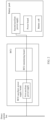
- FIG. 1 is a diagram of a scenario applicable to this application.
- a photovoltaic module converts solar energy into a direct current through a photovoltaic effect.
- a power conversion system converts the direct current from the photovoltaic module into an alternating current, and then outputs the alternating current to a power grid.
- a power conversion system may convert a direct current from an energy storage system into an alternating current, and then output the alternating current to a power grid.
- a power conversion system may convert an alternating current from a power grid into a direct current, and then charge an energy storage system.
- the energy storage system includes a BCU and a battery pack.
- FIG. 2 is a diagram of an energy storage system.
- a BCU includes a BCU-auxiliary power supply board and a BCU-monitoring board.
- the BCU-auxiliary power supply board includes a first auxiliary power supply.
- a battery pack includes a second auxiliary power supply, a power board, and a battery cell.
- One end of the first auxiliary power supply is configured to be connected to a direct current bus of a power conversion system, and the other end of the first auxiliary power supply is connected to the power board through the second auxiliary power supply.
- the first auxiliary power supply obtains power from the direct current bus to supply power to the second auxiliary power supply
- the second auxiliary power supply further provides a direct current with an appropriate voltage for the power board through voltage conversion.
- the BCU-auxiliary power supply board may further include another auxiliary power supply (not shown).
- the another auxiliary power supply may supply power to the BCU-monitoring board, and may also provide some electric energy for the second auxiliary power supply.
- the power board includes a plurality of modules, for example, a sampling module, a monitoring module, and a power conversion module.
- the sampling module is configured to collect current, voltage, or temperature information of the battery cell in a charging/discharging process.
- the monitoring module is configured to transmit information about the battery cell to the BCU.
- the power conversion module is configured to change a charging voltage or a discharging voltage of the battery cell.
- the first auxiliary power supply needs to supply power to the second auxiliary power supply in a cross-device manner, and the first auxiliary power supply is an increase in a power supply path of the second auxiliary power supply.
- the first auxiliary power supply is the increase in the power supply path of the second auxiliary power supply, a probability that a short-circuit fault occurs on the second auxiliary power supply is greatly increased.
- shutdown protection of the energy storage system is triggered. As a result, the energy storage system cannot guide a customer to perform targeted maintenance through an alarm.
- a sampling resistor is disposed on a connection line between the first auxiliary power supply and the second auxiliary power supply.
- a current flowing through the sampling resistor increases, and a voltage between two ends of the sampling resistor increases.
- a sampling circuit transmits a signal of the voltage between the two ends of the sampling resistor to an MCU or a comparison circuit for comparison and determining, to trigger a drive circuit to turn off a main power transistor to disconnect a short-circuit loop.
- this application provides the energy storage system, so that a short-circuit current in the loop when the second auxiliary power supply is short-circuited can be cut off, there is a small quantity of components in the energy storage system, and costs are reduced.
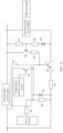
- FIG. 4 is a diagram of an energy storage system according to an embodiment of this application.
- the energy storage system includes a first auxiliary power supply, a battery pack, and a current-limiting protection circuit.
- the first auxiliary power supply is configured to supply power to a second auxiliary power supply in the battery pack
- the second auxiliary power supply is configured to supply power to a power board in the battery pack
- the second auxiliary power supply and the current-limiting protection circuit are connected in series and then connected in parallel to two ends of the first auxiliary power supply.
- the current-limiting protection circuit includes a drive circuit 410, a first switching transistor 420, and a first resistor 430, one end of the first switching transistor 420 and the first resistor 430 that are connected in series is connected to the first auxiliary power supply, the other end of the first switching transistor 420 and the first resistor 430 that are connected in series is connected to the second auxiliary power supply, and the drive circuit 410 is connected to the first auxiliary power supply V1 through the first switching transistor 420 and the first resistor 430; and when a drive voltage is greater than a turn-on voltage of the first switching transistor 420, the first switching transistor 420 is turned on, and the drive voltage is a difference between an output voltage of the drive circuit 410 and a voltage between two ends of the first resistor 430.
- the first switching transistor 420 in this embodiment of this application may be specifically a triode or a metal-oxide semiconductor field-effect transistor (metal-oxide-semiconductor field-effect transistor, MOSFET), or may be an insulated gate bipolar transistor (insulated gate bipolar transistor, IGBT), a gallium nitride (gallium nitride, GaN) high electron mobility transistor (high electron mobility transistor, HEMT), or the like.
- IGBT insulated gate bipolar transistor
- a gallium nitride gallium nitride, GaN
- high electron mobility transistor high electron mobility transistor
- the first resistor 430 in this embodiment of this application may be one resistor, or may include a plurality of resistors connected in series. This is not limited.
- a specific protection process of the energy storage system in this embodiment of this application is as follows: In a normal case, the first switching transistor 420 is turned on, and a loop in which the first auxiliary power supply supplies power to the second auxiliary power supply in the battery pack is turned on, so that the second auxiliary power supply can successfully supply power to the power board in the battery pack.
- the second auxiliary power supply is short-circuited, an increase in a current of the loop in which the first auxiliary power supply supplies power to the second auxiliary power supply causes an increase in the voltage between the two ends of the first resistor 430.
- the drive voltage is the difference between the output voltage of the drive circuit 410 and the voltage between the two ends of the first resistor 430.
- the increase in the voltage between the two ends of the first resistor 430 causes a decrease in the drive voltage of the first switching transistor 420; and when the drive voltage of the first switching transistor 420 is less than the turn-on voltage of the first switching transistor 420, the first switching transistor 420 is turned off, so that a short-circuit current in the loop can be cut off, thereby reducing a risk of short-circuit fault spreading.
- the current-limiting protection circuit in this embodiment of this application includes only the drive circuit 410, the first switching transistor 420, and the first resistor 430. Protection can be implemented through the current-limiting protection circuit.
- the current-limiting protection circuit in this embodiment of this application is simple in design, there is a small quantity of components, and costs and complexity can be reduced.
- the output voltage of the drive circuit 410 in this embodiment of this application is a constant value.
- the voltage output by the drive circuit 410 may not be a constant value.
- a corresponding Zener diode may be disposed, to enable a sum of the drive voltage and the voltage between the two ends of the first resistor 430 to be a constant value.
- the first switching transistor is a triode.
- a base b of the first switching transistor 420 is connected to the drive circuit 410, an emitter e of the first switching transistor 420 is connected to the first resistor R1, and a collector c of the first switching transistor 420 is connected to the second auxiliary power supply.
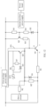
- FIG. 5 is a diagram of another energy storage system according to an embodiment of this application.
- a voltage corresponding to a drive signal output by a drive circuit is small, and a manner in which a first switching transistor Q1 is turned on is as follows: Because an emitter of the first switching transistor Q1 is connected to a negative electrode of a first auxiliary power supply, and a base of Q1 is connected to the drive circuit, when the drive circuit outputs a high-level signal, a base voltage of Q1 is greater than an emitter voltage of Q1; and when a difference between the base voltage of Q1 and the emitter voltage of Q1 is greater than a turn-on voltage of Q1, the first switching transistor Q1 is turned on, that is, a loop in which the first auxiliary power supply supplies power to a second auxiliary power supply in a battery pack is turned on, so that the first auxiliary power supply successfully supplies power to the second auxiliary power supply.
- the turn-on voltage of the first switching transistor Q1 is 3.4 V is used. If a voltage corresponding to the high-level signal output by the drive circuit is 5 V, the voltage is greater than the turn-on voltage of the first switching transistor Q1, so that the first switching transistor Q1 is turned on.
- the voltage output by the drive circuit is a sum of a voltage between two ends of the first resistor R1 and a voltage between the base and the emitter of the first switching transistor Q1. If the second auxiliary power supply is short-circuited, a current flowing through the first resistor R1 increases, the voltage between the two ends of the first resistor R1 increases, and the drive voltage between the base and the emitter of the first switching transistor Q1 decreases.
- the voltage between the base and the emitter of the first switching transistor Q1 is less than the turn-on voltage of the first switching transistor Q1, the first switching transistor Q1 is turned off, so that a short-circuit current in the loop can be cut off, thereby reducing a risk of short-circuit fault spreading.
- a second resistor R2 is connected in series between the drive circuit and the base of the first switching transistor.
- the voltage of the drive signal output by the drive circuit is large. If there is no second resistor R2, the first switching transistor Q1 may be damaged.
- the voltage output by the drive circuit is 48 V
- the voltage of 48 V is applied between the base and the emitter of the first switching transistor Q1 and applied to the first resistor R1.
- the voltage applied between the base and the emitter of the first switching transistor Q1 is large, and may be greater than a limit voltage that can be borne between the base and the emitter of the first switching transistor Q1. As a result, the first switching transistor Q1 is damaged.
- the voltage output by the drive circuit a voltage between two ends of the second resistor R2+the voltage between the base and the emitter of the first switching transistor Q1+the voltage between the two ends of the first resistor R1. Even if the voltage output by the drive circuit is large, the second resistor R2 can bear most of the voltage, to avoid damage to the first switching transistor Q1.
- the turn-on voltage of the first switching transistor Q1 is 3.4 V is still used. If the voltage corresponding to the high-level signal output by the drive circuit is 48 V, and a ratio of a resistance value of the second resistor R2 to the resistance value of the first resistor R1 is 10:1. In this case, if the voltage between the base and the emitter of Q1 is 4 V, the voltage between the two ends of R2 may reach 40 V, and the voltage between the two ends of R1 is 4 V. Because the voltage between the base and the emitter of the first switching transistor Q1 is greater than the turn-on voltage of the first switching transistor Q1, the first switching transistor Q1 is turned on. In addition, because most of the voltage output by the drive circuit is borne by R2, the voltage between the base and the emitter of Q1 is slightly greater than the turn-on voltage of Q1, so that damage to the first switching transistor Q1 can be avoided.
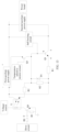
- the voltage output by the drive circuit may not be a constant value. In this case, turn-on or turn-off of the first switching transistor Q1 may be affected. Therefore, as shown in FIG. 7 , in an embodiment, after the first switching transistor Q1 and the first resistor R1 are connected in series, the first switching transistor Q1 and the first resistor R1 are connected in parallel to two ends of a third resistor R2', and one end of the third resistor R2' is connected to the base of the first switching transistor Q1.
- a first Zener diode D1 is further connected in parallel to the two ends of the third resistor R2', and a cathode of the first Zener diode D1 is connected to the base of the first switching transistor Q1.
- functions of R2' and D1 are to stabilize the voltages of Q1 and R1.
- An example in which the turn-on voltage of the first switching transistor Q1 is 3.4 V is still used. If the voltage corresponding to the high-level signal output by the drive circuit is 48 V, and a ratio of the resistance value of the second resistor R2 to a resistance value of the third resistor R2' to the resistance value of the first resistor R1 is 8:4:3, and a Zener voltage value of D1 is 16 V. In this case, because the voltage corresponding to the high level output by the drive circuit is 48 V, the voltage is sufficient to break through the first Zener diode D1. After D1 is broken through, a voltage between two ends of D1 is stabilized at 16 V.
- a sum of the drive voltage of the first switching transistor Q1 and the voltage between the two ends of the first resistor R1 is stabilized at 16 V. If the voltage between the base and the emitter of Q1 is 4 V, the voltage between the two ends of R1 is 12 V. Because the voltage between the base and the emitter of the first switching transistor Q1 is greater than the turn-on voltage of the first switching transistor Q1, the first switching transistor Q1 is turned on.
- the two ends of the third resistor are connected in parallel to the first Zener diode, and the cathode of the first Zener diode is connected to the drive circuit, which is equivalent to that the cathode of the first Zener diode is connected to the drive circuit.
- the voltage corresponding to the high-level signal output by the drive circuit is large, the voltage may break through the first Zener diode.
- the first Zener diode is broken through, the voltage between the two ends of the first Zener diode is a stable voltage value, and the stable voltage value is equivalent to the sum of the drive voltage of the first switching transistor and the voltage between the two ends of the first resistor.
- the voltage between the two ends of the first Zener diode is always a stable voltage value, that is, the sum of the drive voltage of the first switching transistor and the voltage between the two ends of the first resistor is a stable value. Therefore, the voltage between the base and the emitter of the first switching transistor is a stable value, so that the turn-on state of the first switching transistor can be stabilized, and then the first auxiliary power supply may continuously supply power to the second auxiliary power supply in the battery pack.
- the foregoing separately describes a case in which the voltage corresponding to the high-level signal output by the drive circuit is large and a case in which the voltage corresponding to the high-level signal output by the drive circuit is small.
- the signal output by the drive circuit may be a continuous high-level signal, or may be a pulse signal. If the signal output by the drive circuit is a pulse signal, Q1 is periodically turned on and off. This is unfavorable for the first auxiliary power supply to continuously supply power to the second auxiliary power supply in the battery pack.
- the current-limiting protection circuit further includes a self-locking circuit 440, the self-locking circuit 440 is connected in parallel to the second auxiliary power supply, a first end of the self-locking circuit 440 is connected to the first auxiliary power supply, a second end of the self-locking circuit 440 is connected to the collector of the first switching transistor Q1, and a third end of the self-locking circuit 440 is connected to the base of the first switching transistor.
- the drive voltage is greater than the turn-on voltage of the first switching transistor Q1.
- the signal output by the drive circuit is a pulse signal
- Q1 when the signal output by the drive circuit is a pulse signal, Q1 is periodically turned on or off.
- the pulse signal periodically attempts to drive the first switching transistor Q1 to be turned on. After a short-circuit fault is rectified, the first switching transistor Q1 can be automatically turned on without manual intervention, so that self-control of the energy storage system can be improved.
- the drive circuit outputs the pulse signal
- Q1 is periodically turned on or off.
- Q1 is turned off, the loop in which the first auxiliary power supply supplies power to the second auxiliary power supply in the battery pack is disconnected.
- the first auxiliary power supply cannot successfully supply power to the second auxiliary power supply.
- the self-locking circuit 440 in the current-limiting protection circuit in this embodiment of this application can maintain turn-on of the first switching transistor Q1.
- the self-locking circuit is configured to control the drive voltage (namely, the voltage between the base and the emitter of Q1) for driving the first switching transistor to be greater than the turn-on voltage of Q1, to maintain the turn-on state of Q1, so that the first auxiliary power supply can continuously supply power to the second auxiliary power supply in the battery pack.
- the second end of the self-locking circuit 440 is connected to the collector of the first switching transistor Q1, and the third end is connected to the base of the first switching transistor Q1.
- a switching transistor in the self-locking circuit 440 is turned on, it is equivalent to that the base of the first switching transistor Q1 is connected to a positive electrode of the first auxiliary power supply. Because the emitter of the first switching transistor Q1 is connected to the negative electrode of the first auxiliary power supply, the base voltage of the first switching transistor Q1 is greater than the emitter voltage.
- the voltage value of the first auxiliary power supply is appropriate, the voltage between the base and the emitter of the first switching transistor Q1 is greater than the turn-on voltage of the first switching transistor Q1. In this case, the first switching transistor Q1 is turned on, so that the self-locking circuit 440 achieves an objective of maintaining the turn-on state of the first switching transistor Q1.
- the self-locking circuit may maintain the turn-on state of the first switching transistor Q1 when the first switching transistor Q1 is turned on, so that the first auxiliary power supply can continuously supply power to the second auxiliary power supply. If the second auxiliary power supply in the battery pack is short-circuited, the voltage between the two ends of the first resistor R1 increases, and the drive voltage (namely, the voltage between the base and the emitter of Q1) of the first switching transistor Q1 decreases, so that the first switching transistor Q1 is turned off, and the short-circuit current can be cut off, thereby reducing the risk of short-circuit fault spreading.
- FIG. 9 is a diagram of yet another energy storage system according to an embodiment of this application.
- the self-locking circuit 440 in this embodiment of this application includes a second Zener diode D2, a fourth resistor R3, and a second switching transistor Q2.
- the fourth resistor R3 and the second Zener diode D2 are connected in series and then connected in parallel to the second auxiliary power supply, a cathode of the second Zener diode D2 is connected to the fourth resistor R3, an anode of the second Zener diode D2 is connected to the second auxiliary power supply, an emitter of the second switching transistor Q2 is connected to the first auxiliary power supply, a collector of the second switching transistor Q2 is connected to the base of the first switching transistor Q1, and a base of the second switching transistor Q2 is connected to the cathode of the second Zener diode D2.
- the loop in which the first auxiliary power supply supplies power to the second auxiliary power supply in the battery pack is turned on, and the voltage between the two ends of the second auxiliary power supply is equal to a voltage obtained after the resistor R3 is connected in series to the second Zener diode D2.
- a voltage output by the first auxiliary power supply is 48 V, and a turn-on voltage of Q2 is 3.4 V is used.
- the first auxiliary power supply supplies power to the second auxiliary power supply in the battery pack, it is assumed that the voltage between the two ends of the second auxiliary power supply is 36 V.
- a stable voltage of the second Zener diode is 32 V
- the 48 V voltage breaks through the second Zener diode D2, so that the voltage of the second Zener diode D2 is stabilized at 32 V.
- the voltage between the two ends of R3 is 4 V. Because the two ends of R3 are respectively connected to the base of Q2 and the emitter of Q2, and an emitter voltage of Q2 is greater than a base voltage of Q2, Q2 is turned on.
- the collector of Q2 is connected to the base of Q1, when Q2 is turned on, it is equivalent to that the base of Q1 is connected to the first auxiliary power supply, that is, the base voltage of Q1 is always greater than the emitter voltage of Q1, so that the turn-on state of Q1 can be maintained.
- FIG. 10 is a diagram of another energy storage system according to an embodiment of this application.
- the self-locking circuit 440 further includes a fifth resistor R4, the fifth resistor R4 is connected in series between the fourth resistor R3 and the second Zener diode D2, one end of the fifth resistor R4 is connected to the base of the second switching transistor Q2, and the other end of the fifth resistor R4 is connected to the cathode of the second Zener diode D2.
- a limitation on selection of the second Zener diode D2 is reduced.
- a stable voltage of the second Zener diode D2 in this embodiment of this application may be selected as 16 V.
- An example in which a voltage output by the first auxiliary power supply is 48 V, and a turn-on voltage of Q2 is 3.4 V is still used.
- the first auxiliary power supply supplies power to the second auxiliary power supply in the battery pack, it is assumed that the voltage between the two ends of the second auxiliary power supply is 36 V.
- the 48 V voltage breaks through D2, so that the voltage of D2 is stabilized at 16 V. In this case, the voltages of R3 and R4 are 20 V.
- a resistance value of the fourth resistor R3 is 1 ⁇
- a resistance value of the fifth resistor R4 is 5 ⁇
- voltages between two ends of R3 and R4 are respectively 4 V and 16 V. Because the voltage between the two ends of R3 is 4 V, to be specific, the voltage between the base and the emitter of Q2 is 4 V, which is greater than the turn-on voltage of Q2, Q2 is turned on.
- the collector of Q2 is connected to the base of Q1, when Q2 is turned on, it is equivalent to that the base of Q1 is connected to the first auxiliary power supply, that is, the base voltage of Q1 is always greater than the emitter voltage of Q1, so that the turn-on state of Q1 can be maintained.
- selection of the second Zener diode D2 may be slightly relaxed, that is, a Zener diode with a small Zener voltage value may be selected.
- the self-locking circuit 440 further includes a sixth resistor R5, one end of the sixth resistor R5 is connected to the collector of the second switching transistor Q2, and the other end of the sixth resistor R5 is connected to the base of the first switching transistor Q1.
- the sixth resistor R5 in this embodiment of this application may protect Q1. Specifically, when Q2 is turned on, the voltage of the first auxiliary power supply is directly applied between the base and the emitter of Q1, and may exceed a limit voltage between the base and the emitter of Q1. Consequently, this easily causes damage to Q1. When R5 is disposed, R5 may share a part of the voltage, and the voltage between the base and the emitter of Q1 decreases, so that a risk of damage to Q1 can be reduced, and a service life of Q1 can be prolonged.
- the self-locking circuit further includes a capacitor, two ends of the capacitor are respectively connected to the base of the first auxiliary power supply and the base of the second switching transistor, and the capacitor is configured to filter out a clutter of the auxiliary power supply.
- the auxiliary power supply outputs a direct current
- the capacitor may filter out the clutter of the auxiliary power supply, so that a current input to the battery pack is a direct current, thereby reducing interference of the clutter.
- the short-circuit current in the loop may be disconnected by turning off Q1.
- the current-limiting protection circuit in this embodiment of this application may further include a temperature detection circuit, and Q1 is turned off through the temperature detection circuit.
- Strong short circuit and “weak short circuit” in this embodiment of this application are two relative concepts.
- “Strong short circuit” may be understood as that a short-circuit current is quite large. In this case, the voltage between the two ends of the first resistor R1 is large. As a result, the drive voltage of Q1 is less than the turn-on voltage of Q1, and Q1 is turned off.
- "Weak short circuit” may be understood as that a short-circuit current is small.
- the voltage between the two ends of the first resistor R1 increases, an increased amplitude is insufficient to enable the drive voltage of Q1 to be less than the turn-on voltage of the first resistor R1, that is, the transistor Q1 is still in the turn-on state. In this case, for details on how to turn off Q1, refer to descriptions below.
- the current-limiting protection circuit further includes a temperature detection circuit 450
- the temperature detection circuit 450 includes a temperature-sensitive resistor circuit and a third switching transistor Q3, a base of the third switching transistor Q3 is connected to the temperature-sensitive resistor circuit, an emitter of the third switching transistor Q3 is connected in series to the emitter of the first switching transistor Q1, and a collector of the third switching transistor Q3 is connected to the base of the first switching transistor Q1.
- the third switching transistor Q3 When a temperature of the first switching transistor Q1 is greater than a temperature threshold, the third switching transistor Q3 is turned on, and the first switching transistor Q1 is turned off.
- a voltage source of the temperature-sensitive resistor circuit may be a specific voltage source, and the voltage source may be an auxiliary power supply other than the first auxiliary power supply on the BCU-auxiliary power supply board.
- the first switching transistor Q1 is turned on, the loop in which the first auxiliary power supply supplies power to the second auxiliary power supply in the battery pack is turned on, and the first auxiliary power supply successfully supplies power to the second auxiliary power supply in the battery pack.
- a weak short circuit occurs on the second auxiliary power supply, that is, the short-circuit current in the loop in which the first auxiliary power supply supplies power to the second auxiliary power supply is small, although the voltage between the two ends of R1 increases, an increased amplitude of the voltage is insufficient to enable the voltage between the base and the emitter of Q1 to be less than the turn-on voltage of Q1.
- the temperature of Q1 increases.
- the temperature detection circuit 450 detects that the temperature of Q1 exceeds the temperature threshold, and the temperature detection circuit 450 may turn on the third switching transistor Q3. Because the emitter of Q3 is connected to the negative electrode of the first auxiliary power supply, it is equivalent to that the base of Q1 is connected to the negative electrode of the first auxiliary power supply. In addition, because the emitter of Q1 is also connected to the negative electrode of the first auxiliary power supply, the base voltage of Q1 is consistent with the emitter voltage of Q1, so that Q1 can be turned off.
- a setting of the temperature threshold in this embodiment of this application is related to a type of the switching transistor. Temperature thresholds of different types of switching transistors may be the same or may be different.
- the temperature detection circuit may turn on the third switching transistor, to enable the first switching transistor to be turned off, so that damage to the first switching transistor caused by an excessively high temperature can be avoided, thereby protecting the first switching transistor, and prolonging a service life of the first switching transistor.
- the temperature detection circuit is used to protect the first switching transistor against the weak short circuit occurred on the second auxiliary power supply in the battery pack, during actual application, the temperature detection circuit can still protect the first switching transistor against a strong short circuit occurred on the battery pack. Therefore, the temperature detection circuit provided in this embodiment of this application can adapt to various short-circuit scenarios. To be specific, for various short-circuit cases of the second auxiliary power supply in the battery pack, the temperature detection circuit can protect the first switching transistor.
- the temperature-sensitive resistor circuit 450 includes a temperature-sensitive resistor, a seventh resistor, an eighth resistor, and a third Zener diode, and a resistance value of the temperature-sensitive resistor decreases as the temperature of the first switching transistor increases.
- the temperature-sensitive resistor and the seventh resistor are connected in series and then connected to the emitter of the third switching transistor Q3, the third Zener diode and the eighth resistor are connected in series and then connected in parallel to two ends of the seventh resistor, and a connection point between the third Zener diode and the seventh resistor is connected to the base of the third switching transistor.
- the temperature-sensitive resistor is RT1
- the seventh resistor is R6
- the eighth resistor is R7
- the third Zener diode is D3
- a resistance value of the temperature-sensitive resistor RT1 decreases as the temperature increases.
- the second auxiliary power supply in the battery pack is short-circuited, there is the short-circuit current in the loop.
- the short-circuit current flows through the first switching transistor Q1, causing the temperature of the first switching transistor Q1 to increase, and the resistance value of the temperature-sensitive resistor RT1 decreases, causing a voltage between two ends of RT1 to decrease.
- a voltage between the two ends of the seventh resistor R6 increases.
- the third Zener diode D3 and the resistor R7 are connected in series, the third Zener diode D3 and the resistor R7 are connected in parallel to the two ends of the resistor R6.
- the voltage between the two ends of the resistor R6 is voltage obtained after the third Zener diode D3 and the resistor R7 are connected in series.
- An increase in the voltage between the two ends of the resistor R6 is equivalent to an increase in the voltage obtained after the third Zener diode D3 and the resistor R7 are connected in series.
- the third Zener diode D3 may be broken through. After the third Zener diode D3 is broken through, the voltage between the two ends of the third Zener diode D3 is a stable voltage value, for example, is stabilized at 4 V.
- a base voltage of the third switching transistor Q3 is 4 V, which is greater than an emitter voltage of the third switching transistor Q3, and the third switching transistor Q3 is turned on.
- the third switching transistor Q3 is turned on, because the emitter of the third switching transistor Q3 is connected to the negative electrode of the first auxiliary power supply and the collector of the third switching transistor Q3 is connected to the base of the first switching transistor Q1, it is equivalent to that the base of the first switching transistor Q1 is connected to the negative electrode of the first auxiliary power supply.
- the emitter of Q1 is also connected to the negative electrode of the first auxiliary power supply, the base voltage of the first switching transistor Q1 is consistent with the emitter voltage of the first switching transistor Q1, so that the first switching transistor Q1 can be turned off, to protect the first switching transistor Q1.
- the drive circuit and a main circuit (where the main circuit may be understood as a circuit in which the first auxiliary power supply supplies power to the second auxiliary power supply in the battery pack) share the negative electrode is used.
- the drive circuit and the main circuit may alternatively not share the negative electrode, that is, the drive circuit is isolated from the main circuit.
- FIG. 13 is a diagram of yet another energy storage system according to an embodiment of this application.
- the capacitor C can transmit the pulse signal due to a direct current blocking and alternating current characteristic of the capacitor C.
- the drive circuit is connected to the base of the switching transistor Q4, and the emitter of the switching transistor Q4 is grounded. Therefore, when the drive circuit outputs the high-level signal, the switching transistor Q4 is turned on, so that the voltage source is turned on by using a primary side of an optical coupler U and a circuit of the switching transistor Q4.
- the voltage output by the voltage source acts on the primary side of the optical coupler U (that is, on a light-emitting diode of the optical coupler U shown in the figure), so that the light-emitting diode emits light.
- the light-emitting diode may enable a secondary side of the optical coupler U (namely, a switching transistor of the optical coupler U shown in the figure) to be turned on, so that the first auxiliary power supply forms a loop through the secondary side of the optical coupler U, R2, Q1, and R1, and Q1 is turned on.
- the resistor R9 shown in FIG. 13 is configured to protect the switching transistor Q4.
- a voltage between the base and the emitter of the switching transistor Q4 is the voltage between the two ends of the resistor R9, to avoid damage to the switching transistor Q4 caused by an excessively large voltage between the base and the emitter of the switching transistor Q4.
- the voltage source is grounded through the switching transistor Q4, and the first auxiliary power supply is connected to the negative electrode of the first auxiliary power supply V1 through the second auxiliary power supply in the battery pack, the first switching transistor Q1, and the first resistor R1.
- the two voltage sources are not grounded together. In other words, the voltage source is isolated from the circuit in which the first auxiliary power supply supplies power to the second auxiliary power supply in the battery pack.
- the photovoltaic energy storage system includes a power converter and the energy storage system according to any one of the foregoing embodiments, a direct current input end of the power converter is configured to be connected to a photovoltaic module, an alternating current output end of the power converter is configured to be connected to a load, the power converter includes a direct current conversion circuit and an inverter circuit that are connected in series, and a series connection point between the direct current conversion circuit and the inverter circuit is connected to the first auxiliary power supply of the energy storage system.
- the photovoltaic module converts solar energy into a direct current through a photovoltaic effect.
- a power conversion system converts the direct current into an alternating current, and then sends the alternating current to a power grid.
- a power conversion system may convert a direct current from the energy storage system into an alternating current, and then send the alternating current to a power grid.
- the power converter in this embodiment of this application may be the power conversion system in FIG. 1 .
- the energy storage system includes a BCU and a battery pack, the energy storage system is connected to a direct current bus in the power conversion system, and the BCU in the energy storage system may obtain power from the direct current bus in the power conversion system, and process a direct current to output different voltages. For example, a voltage of 48 V obtained after the processing may be used to supply power to a second auxiliary power supply in the battery pack.
- this application may be applied to any scenario including a power supply and a load.
- this application further provides an inverter system.
- the inverter system includes a power converter and a backup power box.
- the power converter is configured to convert a direct current from a direct current source into an alternating current, and transmits the alternating current to the backup power box.
- a first auxiliary power supply in the power converter is configured to supply power to the second auxiliary power supply in the backup power box. After the second auxiliary power supply and a current-limiting protection circuit are connected in series, the second auxiliary power supply and the current-limiting protection circuit are connected in parallel to two ends of the first auxiliary power supply.
- the current-limiting protection circuit includes a drive circuit, a first switching transistor, and a first resistor, one end of the first switching transistor and the first resistor that are connected in series is connected to the first auxiliary power supply, the other end of the first switching transistor and the first resistor that are connected in series is connected to the second auxiliary power supply, and the drive circuit is connected to the first auxiliary power supply through the first switching transistor and the first resistor; and when a drive voltage is greater than a turn-on voltage of the first switching transistor, the first switching transistor is turned on, and the drive voltage is a difference between an output voltage of the drive circuit and a voltage between two ends of the first resistor.
- the first auxiliary power supply in the power converter is equivalent to the first auxiliary power supply in the foregoing embodiments
- the backup power box is equivalent to the battery pack in the foregoing embodiments
- the second auxiliary power supply in the backup power box is equivalent to the second auxiliary power supply in the battery pack.
- this application further provides an electric vehicle.
- the electric vehicle may include an auxiliary power supply and a battery pack, and the auxiliary power supply is configured to supply power to the auxiliary power supply in the battery pack.
- the auxiliary power supply in the battery pack and a current-limiting protection circuit are connected in series, the auxiliary power supply and the current-limiting protection circuit are connected in parallel to two ends of the auxiliary power supply.
- the current-limiting protection circuit includes a drive circuit, a first switching transistor, and a first resistor, one end of the first switching transistor and the first resistor that are connected in series is connected to the auxiliary power supply, the other end of the first switching transistor and the first resistor that are connected in series is connected to the auxiliary power supply in the battery pack, and the drive circuit is connected to the auxiliary power supply through the first switching transistor and the first resistor; and when a drive voltage is greater than a turn-on voltage of the first switching transistor, the first switching transistor is turned on, and the drive voltage is a difference between an output voltage of the drive circuit and a voltage between two ends of the first resistor.
- auxiliary power supply in this embodiment of this application is equivalent to the first auxiliary power supply in the foregoing embodiments, and the auxiliary power supply in the battery pack is equivalent to the second auxiliary power supply in the foregoing embodiments.
- a specific circuit connection relationship and a protection process are similar to those in the foregoing embodiments. Details are not described again.
Landscapes
- Engineering & Computer Science (AREA)
- Power Engineering (AREA)
- Protection Of Static Devices (AREA)
- Charge And Discharge Circuits For Batteries Or The Like (AREA)
- Stand-By Power Supply Arrangements (AREA)
- Dc-Dc Converters (AREA)
Applications Claiming Priority (1)
| Application Number | Priority Date | Filing Date | Title |
|---|---|---|---|
| CN202311648277.0A CN118074062A (zh) | 2023-12-04 | 2023-12-04 | 储能系统和光储系统 |
Publications (2)
| Publication Number | Publication Date |
|---|---|
| EP4568050A2 true EP4568050A2 (de) | 2025-06-11 |
| EP4568050A3 EP4568050A3 (de) | 2025-07-30 |
Family
ID=91104836
Family Applications (1)
| Application Number | Title | Priority Date | Filing Date |
|---|---|---|---|
| EP24215636.2A Pending EP4568050A3 (de) | 2023-12-04 | 2024-11-27 | Energiespeichersystem und photovoltaisches energiespeichersystem |
Country Status (3)
| Country | Link |
|---|---|
| US (1) | US20250183659A1 (de) |
| EP (1) | EP4568050A3 (de) |
| CN (1) | CN118074062A (de) |
Family Cites Families (2)
| Publication number | Priority date | Publication date | Assignee | Title |
|---|---|---|---|---|
| CN102694403B (zh) * | 2012-05-30 | 2015-01-21 | 江苏科技大学 | 一种充电器及其控制方法 |
| CN110198064A (zh) * | 2019-06-26 | 2019-09-03 | 深圳市道通智能航空技术有限公司 | 一种供电的控制电路、方法及充电器 |
-
2023
- 2023-12-04 CN CN202311648277.0A patent/CN118074062A/zh active Pending
-
2024
- 2024-11-27 EP EP24215636.2A patent/EP4568050A3/de active Pending
- 2024-12-02 US US18/965,118 patent/US20250183659A1/en active Pending
Also Published As
| Publication number | Publication date |
|---|---|
| US20250183659A1 (en) | 2025-06-05 |
| CN118074062A (zh) | 2024-05-24 |
| EP4568050A3 (de) | 2025-07-30 |
Similar Documents
| Publication | Publication Date | Title |
|---|---|---|
| US9246402B2 (en) | Converter and semiconductor device | |
| EP3817232B1 (de) | Ansteuerungsschaltung für nmos-schalter und stromversorgungsvorrichtung | |
| CN112134466B (zh) | 原边控制电路、功率变换器及其控制方法 | |
| KR20120112734A (ko) | 전력 라인의 전류를 제한하고 및/또는 차단하는 스위칭 모듈 | |
| CN214900648U (zh) | 一种电源管理芯片及开关电源管理系统 | |
| US20250047119A1 (en) | Battery pack with a bi-directional switch and associated driver circuit and control method | |
| US11114890B2 (en) | DC uninterruptible power supply apparatus with bidirectional protection function | |
| US12132304B2 (en) | Over-energy protection circuit, residual current device, electronic device, and power distribution box | |
| US11831264B2 (en) | Power supply system of motor control module and vehicle | |
| CN114914995A (zh) | 一种用于移动服务机器人的充电过压保护电路 | |
| CN110707764B (zh) | 用于opgw监测的感应取电系统 | |
| EP4568050A2 (de) | Energiespeichersystem und photovoltaisches energiespeichersystem | |
| WO2021000253A1 (en) | Photovoltaic system and control method thereof | |
| WO2023125826A1 (zh) | 双向充电管理系统及其电池监管设备 | |
| CN115498719A (zh) | 充电保护电路、方法、电池管理系统、电池包及用电装置 | |
| US20230406136A1 (en) | Detection Circuit, Anti-Backflow System, and Charging Pile | |
| CN214255774U (zh) | 一种电池充电休眠控制电路 | |
| US6608769B2 (en) | Switched mode power supply with a device for limiting the output voltage | |
| CN119891708B (zh) | 功率半导体器件的驱动取能系统及驱动取能方法 | |
| EP4579980A1 (de) | Energiespeichersystem und heizsteuerungsverfahren für batteriepack | |
| CN211790898U (zh) | 充电控制电路及充电控制装置 | |
| CN219477613U (zh) | 一种车载单元充电电路及车载单元 | |
| US20240380349A1 (en) | Motor controller and powertrain | |
| CN223502615U (zh) | 启停控制装置及电力系统 | |
| CN221113535U (zh) | 主动放电电路、电机控制器及电动车辆 |
Legal Events
| Date | Code | Title | Description |
|---|---|---|---|
| PUAI | Public reference made under article 153(3) epc to a published international application that has entered the european phase |
Free format text: ORIGINAL CODE: 0009012 |
|
| STAA | Information on the status of an ep patent application or granted ep patent |
Free format text: STATUS: THE APPLICATION HAS BEEN PUBLISHED |
|
| AK | Designated contracting states |
Kind code of ref document: A2 Designated state(s): AL AT BE BG CH CY CZ DE DK EE ES FI FR GB GR HR HU IE IS IT LI LT LU LV MC ME MK MT NL NO PL PT RO RS SE SI SK SM TR |
|
| PUAL | Search report despatched |
Free format text: ORIGINAL CODE: 0009013 |
|
| AK | Designated contracting states |
Kind code of ref document: A3 Designated state(s): AL AT BE BG CH CY CZ DE DK EE ES FI FR GB GR HR HU IE IS IT LI LT LU LV MC ME MK MT NL NO PL PT RO RS SE SI SK SM TR |
|
| RIC1 | Information provided on ipc code assigned before grant |
Ipc: H02J 3/32 20060101AFI20250626BHEP Ipc: H02H 7/18 20060101ALI20250626BHEP Ipc: H02J 3/38 20060101ALI20250626BHEP Ipc: H02J 7/00 20060101ALI20250626BHEP |