EP4567902A1 - Solarzelle und herstellungsverfahren dafür - Google Patents
Solarzelle und herstellungsverfahren dafür Download PDFInfo
- Publication number
- EP4567902A1 EP4567902A1 EP23848852.2A EP23848852A EP4567902A1 EP 4567902 A1 EP4567902 A1 EP 4567902A1 EP 23848852 A EP23848852 A EP 23848852A EP 4567902 A1 EP4567902 A1 EP 4567902A1
- Authority
- EP
- European Patent Office
- Prior art keywords
- amorphous silicon
- conductive film
- transparent conductive
- hole
- electrode
- Prior art date
- Legal status (The legal status is an assumption and is not a legal conclusion. Google has not performed a legal analysis and makes no representation as to the accuracy of the status listed.)
- Pending
Links
Images


Classifications
-
- H—ELECTRICITY
- H10—SEMICONDUCTOR DEVICES; ELECTRIC SOLID-STATE DEVICES NOT OTHERWISE PROVIDED FOR
- H10F—INORGANIC SEMICONDUCTOR DEVICES SENSITIVE TO INFRARED RADIATION, LIGHT, ELECTROMAGNETIC RADIATION OF SHORTER WAVELENGTH OR CORPUSCULAR RADIATION
- H10F77/00—Constructional details of devices covered by this subclass
- H10F77/20—Electrodes
- H10F77/206—Electrodes for devices having potential barriers
- H10F77/211—Electrodes for devices having potential barriers for photovoltaic cells
-
- H—ELECTRICITY
- H10—SEMICONDUCTOR DEVICES; ELECTRIC SOLID-STATE DEVICES NOT OTHERWISE PROVIDED FOR
- H10F—INORGANIC SEMICONDUCTOR DEVICES SENSITIVE TO INFRARED RADIATION, LIGHT, ELECTROMAGNETIC RADIATION OF SHORTER WAVELENGTH OR CORPUSCULAR RADIATION
- H10F10/00—Individual photovoltaic cells, e.g. solar cells
- H10F10/10—Individual photovoltaic cells, e.g. solar cells having potential barriers
- H10F10/16—Photovoltaic cells having only PN heterojunction potential barriers
- H10F10/164—Photovoltaic cells having only PN heterojunction potential barriers comprising heterojunctions with Group IV materials, e.g. ITO/Si or GaAs/SiGe photovoltaic cells
- H10F10/165—Photovoltaic cells having only PN heterojunction potential barriers comprising heterojunctions with Group IV materials, e.g. ITO/Si or GaAs/SiGe photovoltaic cells the heterojunctions being Group IV-IV heterojunctions, e.g. Si/Ge, SiGe/Si or Si/SiC photovoltaic cells
- H10F10/166—Photovoltaic cells having only PN heterojunction potential barriers comprising heterojunctions with Group IV materials, e.g. ITO/Si or GaAs/SiGe photovoltaic cells the heterojunctions being Group IV-IV heterojunctions, e.g. Si/Ge, SiGe/Si or Si/SiC photovoltaic cells the Group IV-IV heterojunctions being heterojunctions of crystalline and amorphous materials, e.g. silicon heterojunction [SHJ] photovoltaic cells
-
- H—ELECTRICITY
- H10—SEMICONDUCTOR DEVICES; ELECTRIC SOLID-STATE DEVICES NOT OTHERWISE PROVIDED FOR
- H10F—INORGANIC SEMICONDUCTOR DEVICES SENSITIVE TO INFRARED RADIATION, LIGHT, ELECTROMAGNETIC RADIATION OF SHORTER WAVELENGTH OR CORPUSCULAR RADIATION
- H10F71/00—Manufacture or treatment of devices covered by this subclass
- H10F71/10—Manufacture or treatment of devices covered by this subclass the devices comprising amorphous semiconductor material
- H10F71/103—Manufacture or treatment of devices covered by this subclass the devices comprising amorphous semiconductor material including only Group IV materials
-
- H—ELECTRICITY
- H10—SEMICONDUCTOR DEVICES; ELECTRIC SOLID-STATE DEVICES NOT OTHERWISE PROVIDED FOR
- H10F—INORGANIC SEMICONDUCTOR DEVICES SENSITIVE TO INFRARED RADIATION, LIGHT, ELECTROMAGNETIC RADIATION OF SHORTER WAVELENGTH OR CORPUSCULAR RADIATION
- H10F71/00—Manufacture or treatment of devices covered by this subclass
- H10F71/138—Manufacture of transparent electrodes, e.g. transparent conductive oxides [TCO] or indium tin oxide [ITO] electrodes
- H10F71/1385—Etching transparent electrodes
-
- H—ELECTRICITY
- H10—SEMICONDUCTOR DEVICES; ELECTRIC SOLID-STATE DEVICES NOT OTHERWISE PROVIDED FOR
- H10F—INORGANIC SEMICONDUCTOR DEVICES SENSITIVE TO INFRARED RADIATION, LIGHT, ELECTROMAGNETIC RADIATION OF SHORTER WAVELENGTH OR CORPUSCULAR RADIATION
- H10F77/00—Constructional details of devices covered by this subclass
- H10F77/10—Semiconductor bodies
- H10F77/16—Material structures, e.g. crystalline structures, film structures or crystal plane orientations
- H10F77/162—Non-monocrystalline materials, e.g. semiconductor particles embedded in insulating materials
- H10F77/166—Amorphous semiconductors
- H10F77/1662—Amorphous semiconductors including only Group IV materials
-
- H—ELECTRICITY
- H10—SEMICONDUCTOR DEVICES; ELECTRIC SOLID-STATE DEVICES NOT OTHERWISE PROVIDED FOR
- H10F—INORGANIC SEMICONDUCTOR DEVICES SENSITIVE TO INFRARED RADIATION, LIGHT, ELECTROMAGNETIC RADIATION OF SHORTER WAVELENGTH OR CORPUSCULAR RADIATION
- H10F77/00—Constructional details of devices covered by this subclass
- H10F77/20—Electrodes
- H10F77/206—Electrodes for devices having potential barriers
- H10F77/211—Electrodes for devices having potential barriers for photovoltaic cells
- H10F77/215—Geometries of grid contacts
-
- H—ELECTRICITY
- H10—SEMICONDUCTOR DEVICES; ELECTRIC SOLID-STATE DEVICES NOT OTHERWISE PROVIDED FOR
- H10F—INORGANIC SEMICONDUCTOR DEVICES SENSITIVE TO INFRARED RADIATION, LIGHT, ELECTROMAGNETIC RADIATION OF SHORTER WAVELENGTH OR CORPUSCULAR RADIATION
- H10F77/00—Constructional details of devices covered by this subclass
- H10F77/20—Electrodes
- H10F77/206—Electrodes for devices having potential barriers
- H10F77/211—Electrodes for devices having potential barriers for photovoltaic cells
- H10F77/219—Arrangements for electrodes of back-contact photovoltaic cells
-
- H—ELECTRICITY
- H10—SEMICONDUCTOR DEVICES; ELECTRIC SOLID-STATE DEVICES NOT OTHERWISE PROVIDED FOR
- H10F—INORGANIC SEMICONDUCTOR DEVICES SENSITIVE TO INFRARED RADIATION, LIGHT, ELECTROMAGNETIC RADIATION OF SHORTER WAVELENGTH OR CORPUSCULAR RADIATION
- H10F77/00—Constructional details of devices covered by this subclass
- H10F77/20—Electrodes
- H10F77/244—Electrodes made of transparent conductive layers, e.g. transparent conductive oxide [TCO] layers
Definitions
- the present application relates to the field of photovoltaic technology, in particular to a solar cell and a preparation method therefor.
- heterojunction cells Compared to BSF cells and PERC structured cells, heterojunction cells (HJT, also referred to heterojunction with intrinsic thin layer), represent a more efficient type of crystalline silicon solar cell currently. These cells combine the advantages of crystalline silicon cells and silicon-based thin film cells, offering benefits such as a shorter manufacturing process, a lower processing temperature, a relatively high conversion efficiency, and a greater power generation capacity.
- a typical heterojunction cell includes several layers arranged from top to bottom: a front electrode, a front transparent conductive film layer, a front doped amorphous silicon layer, a front intrinsic amorphous silicon layer, a monocrystalline silicon substrate, a back intrinsic amorphous silicon layer, a back doped amorphous silicon layer, a back transparent conductive film layer, and a back electrode.
- the structure of a conventional heterojunction cell is illustrated in FIG. 2 .
- the front electrode contacts the front transparent conductive film layer, while the back electrode contacts the back transparent conductive film layer.
- the front and back electrodes During carrier collection by the front and back electrodes, carriers primarily transfer in the front and back transparent conductive film layers.
- the photoelectric conversion efficiency of the heterojunction cell with this structure still requires further improvement.
- an objective of the present application is to provide a solar cell having a high photoelectric conversion efficiency.
- the solar cell includes:
- the electrode is disposed on the transparent conductive film layer and in direct contact with the doped amorphous silicon layer, such that the electrode is not only in contact with the transparent conductive film layer, but also in direct contact with the doped amorphous silicon layer.
- the electrode During carrier collection by the electrode, a part of the carriers can be collected in the doped amorphous silicon film layer, which reduces the transfer distance for the carriers in the transparent conductive film layer and decreases the transverse resistance, thereby increasing the photoelectric conversion efficiency of the solar cell.
- the transparent conductive film layer is provided with a through-hole, and a part of the electrode is embedded in the through-hole and in direct contact with the doped amorphous silicon layer.
- a width of the through-hole is less than or equal to a width of the part of the electrode that is not embedded in the through-hole. This ensures excellent contact between the electrode and the transparent conductive film layer, thereby decreasing the resistance to the carriers transferred between the transparent conductive film layer and the electrode, and further increasing the photoelectric conversion efficiency of the solar cell.
- the part of the electrode that is embedded in the through-hole is in contact with a side wall of the through-hole. This further ensures excellent contact between the electrode and the transparent conductive film layer, thereby further decreasing the resistance to the carriers transferred between the transparent conductive film layer and the electrode, and further increasing the photoelectric conversion efficiency of the solar cell.
- a ratio of an area of the through-hole to a bottom area of the part of the electrode that is not embedded in the through-hole is (0.94-0.98): 1.
- the through-hole is either a strip-shaped hole or a plurality of dot-shaped holes arranged at intervals.
- the dot-shaped holes include a circular hole, an elliptical hole, a square hole, a rectangular hole, or any combination thereof.
- a preparation method for a solar cell includes:
- the electrode can be not only in contact with the transparent conductive film layer, but also in direct contact with the doped amorphous silicon layer.
- a part of the carriers can be collected in the doped amorphous silicon film layer, which reduces the transfer distance for the carriers in the transparent conductive film layer and decreases the transverse resistance, thereby increasing the photoelectric conversion efficiency of the solar cell.
- the forming the transparent conductive film layer on the doped amorphous silicon layer includes: depositing the transparent conductive film layer on the doped amorphous silicon layer by using a mask with a shielding region to form a through-hole for the electrode to be embedded in, at a region of the transparent conductive film layer corresponding to the shielding region.
- the transparent conductive film layer with a through-hole in a specific shape is deposited and formed on the doped amorphous silicon layer by using the mask with a specific shielding region, such that the electrode can be in direct contact with doped amorphous silicon layer by passing through the through-hole.
- the preparation method is simple to operate, and the prepared electrode is in excellent contact with the doped amorphous silicon layer, the transparent conductive film layer and inner side wall of the through-hole, thereby further decreasing the resistance and increasing the photoelectric conversion efficiency of the heterojunction cell.
- the method further includes perforating the transparent conductive film layer to form a through-hole for the electrode to be embedded in, in the transparent conductive film layer after the transparent conductive film layer is formed and before the electrode is prepared.
- the transparent conductive film layer is prepared firstly and then perforated to provide the through-hole for the electrode to be embedded in, which makes the preparation method simple in operation.
- the perforating is performed by solution etching, laser etching, or a combination thereof.
- the preparing the electrode on the transparent conductive film layer includes: printing an electrode paste at the through-hole in the transparent conductive film layer by screen printing, ensuing that the through-hole is filled with the electrode paste, and then solidifying the electrode paste.
- the intrinsic amorphous silicon layer is formed on the monocrystalline silicon substrate through a plasma enhanced chemical vapor deposition method.
- the doped amorphous silicon layer is formed on the intrinsic amorphous silicon layer through a plasma enhanced chemical vapor deposition method.
- the transparent conductive film layer is formed on the doped amorphous silicon layer through a physical vapor deposition method.
- the method further includes: texturing the monocrystalline silicon substrate before the forming the intrinsic amorphous silicon layer on the monocrystalline silicon substrate.
- the solar cell of the present application is obtained by modifying the structure of the conventional heterojunction cell so that the electrode of the heterojunction cell is in direct contact with the doped amorphous silicon layer.
- the electrode can be not only in contact with the transparent conductive film layer, but also in direct contact with the doped amorphous silicon layer.
- carrier collection by the electrode not only the carriers can be transferred into the electrode through the transparent conductive film layer, but a part of the carriers can be collected in the doped amorphous silicon film layer and then transferred into the electrode, which reduce the transfer distance for the carriers in the transparent conductive film layer and reduces the transverse resistance, thereby increasing the photoelectric conversion efficiency of the heterojunction solar cell.
- first and second are merely for description and cannot be interpreted as indicating or implying relative importance or implicitly indicating the number or order of technical features indicated. Therefore, the features defined with “first” and “second” can explicitly or implicitly include at least one feature. In the description of the present application, "a plurality of” means at least two, such as two or three unless definitely and specifically limited otherwise.
- an element such as a layer, film or substrate is referred to as being “on” another film layer
- the element can be directly on the other film layer, or intermediate film layers may be provided.
- the layer may be directly below the other layer, or one or more intermediate layers may be provided. It can also be understood that when a layer is referred to as being “between” two layers, the layer may be the only one between the two layers, or one or more intermediate layers may be provided.
- the solar cell 10 includes, in order from a front surface to a back surface, a front electrode 11, a front transparent conductive film layer 12, a front doped amorphous silicon layer 13, a front intrinsic amorphous silicon layer 14, a monocrystalline silicon substrate 15, a back intrinsic amorphous silicon layer 16, a back doped amorphous silicon layer 17, a back transparent conductive film layer 18, and a back electrode 19.
- the front electrode 11 is in direct contact with the front doped amorphous silicon layer 13.
- the back electrode 19 is in direct contact with the back doped amorphous silicon layer 17.
- the front electrode 11 and the back electrode 19 are in contact with the front transparent conductive film layer 12 and the back transparent conductive film layer 18, respectively.
- the carriers primarily transfer in the front transparent conductive film layer 12 and the back transparent conductive film layer 18.
- FIG. 3 A schematic view of a carrier transfer direction in the conventional solar cell 10 is shown in FIG. 3 (a direction indicated by an arrow in FIG. 3 is the carrier transfer direction).
- the structure of the conventional solar cell 10 has been modified in the present application so that the front electrode 11 is in direct contact with the front doped amorphous silicon layer 13, while the back electrode 19 is in direct contact with the back doped amorphous silicon layer 17 in the solar cell 10.
- a part of the carriers can be collected in the doped amorphous silicon film layers, which reduces the transfer distance for the carriers in the transparent conductive film layers and decreases the transverse resistance, thereby increasing the photoelectric conversion efficiency of the solar cell 10.
- the front transparent conductive film layer 12 is provided with a first through-hole 121, and a part of the front electrode 11 is embedded in the first through-hole 121 and in direct contact with the front doped amorphous silicon layer 13.
- the back transparent conductive film layer 18 is provided with a second through-hole 181, and a part of the back electrode 19 is embedded in the second through-hole 181 and in direct contact with the back doped amorphous silicon layer 17.
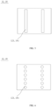
- a width ( a in FIG. 1 ) of the first through-hole 121 is preferably less than or equal to a width (b in FIG. 1 ) of a part of the front electrode 11 that is not embedded in the first through-hole 121, and the front electrode 11 is in contact with a side wall of the first through-hole 121.
- a width (c in FIG. 1 ) of the second through-hole 181 is preferably less than or equal to a width (d in FIG. 1 ) of a part of the back electrode 19 that is not embedded in the second through-hole 181, and the back electrode 19 is in contact with a side wall of the second through-hole 181.
- a ratio of an area of the first through-hole 121 to a bottom area of the part of the front electrode 11 that is not embedded in the first through-hole 121 is (0.94-0.98): 1.
- a ratio of an area of the second through-hole 181 to a bottom area of the part of the back electrode 19 that is not embedded in the second through-hole 181 is (0.94-0.98): 1.
- the first through-hole 121 and the second through-hole 181 may be a strip-shaped hole or a plurality of dot-shaped holes arranged at intervals.
- the dot-shaped holes may be various shapes such as circular holes, elliptical holes, square holes, rectangular holes, etc.
- the shapes of the first through-hole 121 and the second through-hole 181 are not limited thereto, and any through-hole can be used as long as the electrode can pass through the transparent conductive film layer to make direct contact with the doped amorphous silicon layer. Moreover, provided that the width of the through-hole is less than or equal to the width of the electrode, the through-hole can be made appropriately wider, which increases the contact area between the electrode and the doped amorphous silicon layer, thereby reducing the resistance during carrier transfer.
- the specific manner of achieving direct contact between the electrodes and the doped amorphous silicon layers is not limited to the above-mentioned manner of forming the first through-hole 121 and the second through-hole 181 in the front transparent conductive film layer 12 and the back transparent conductive film layer 18.
- Other conventional manners may also be used to establish contact between the front electrode 11 and the front doped amorphous silicon layer 13 and between the back electrode 19 and the back doped amorphous silicon layer 17.
- a preparation method for a solar cell 10 includes S100 to S500.
- the monocrystalline silicon substrate 15 is firstly textured using a texturing chemical solution to form a pyramidal light-trapping structure on a surface of the monocrystalline silicon substrate 15 to reduce the light reflectance on the monocrystalline silicon substrate 15a and increase the light utilization efficiency of the solar cell 10.
- An apparatus and a process for texturing can refer to the conventional texturing and cleaning machines and the conventional texturing procedures.
- a plasma enhanced chemical vapor deposition (PECVD) process may be used to deposit the front intrinsic amorphous silicon layer 14 and the back intrinsic amorphous silicon layer 16 on the front surface and the back surface of the monocrystalline silicon substrate 15, respectively.
- PECVD plasma enhanced chemical vapor deposition
- the specific deposition process conditions for the front intrinsic amorphous silicon layer 14 and the back intrinsic amorphous silicon layer 16 may either follow existing processes or be appropriately adjusted based on existing processes according to actual requirements.
- the thicknesses of both the front intrinsic amorphous silicon layer 14 and the back intrinsic amorphous silicon layer 16 may be determined according to specific needs.
- the front doped amorphous silicon layer 13 may be deposited on a surface of the front intrinsic amorphous silicon layer 14 facing away from the monocrystalline silicon substrate 15 through the PECVD process
- the back doped amorphous silicon layer 17 may be deposited on a surface of the back intrinsic amorphous silicon layer 16 facing away from the monocrystalline silicon substrate 15 through the PECVD process.
- the specific deposition process conditions for the front doped amorphous silicon layer 13 and the back doped amorphous silicon layer 17 may either follow existing processes or be appropriately adjusted based on existing processes according to actual requirements. Thicknesses of both the front doped amorphous silicon layer 13 and the back doped amorphous silicon layer 17 may also be determined according to actual needs.
- the front transparent conductive film layer 12 is deposited on a surface of the front doped amorphous silicon layer 13 facing away from the front intrinsic amorphous silicon layer 14 through a physical vapor deposition (PVD) process
- the back transparent conductive film layer 18 is deposited on a surface of the back doped amorphous silicon layer 17 facing away from the back intrinsic amorphous silicon layer 16 through the PVD process.
- PVD physical vapor deposition
- the front transparent conductive film layer 12 is deposited on the front doped amorphous silicon layer 13 as follows: first, disposing a mask having a shielding region on the front doped amorphous silicon layer 13, and then forming the front transparent conductive film layer 12 on the front doped amorphous silicon layer 13 through the PVD deposition, such that the first through-hole 121 is formed in a region of the front transparent conductive film layer 12 corresponding to the shielding region.
- the back transparent conductive film layer 18 is deposited on the back doped amorphous silicon layer 17 as follows: first, forming the back transparent conductive film layer 18 on the back doped amorphous silicon layer 17 through the PVD deposition by using a mask having a shielding region, such that the second through-hole 181 is formed in a region of the back transparent conductive film layer 18 corresponding to the shielding region.
- the shape of the shielding region on the mask may be determined according to the shape of the first through-hole 121 or the second through-hole 181.
- the first through-hole 121 or the second through-hole 181 is a strip-shaped hole (as shown in FIG. 5 )
- a mask having a strip-shaped shielding region is used.
- the first through-hole 121 or the second through-hole 181 includes dot-shaped holes arranged at intervals (as shown in FIGS. 6 and 7 ), a mask having dot-shaped shielding regions is used.
- the transparent conductive film layer with a through-hole in a specific shape can be conveniently prepared and formed on the doped amorphous silicon layer. Therefore, the electrode can be conveniently in direct contact with the doped amorphous silicon layer through the through-hole after the subsequent preparation of the electrode.
- an intact front transparent conductive film layer 12 and an intact back transparent conductive film layer 18 are deposited on the front doped amorphous silicon layer 13 and the back doped amorphous silicon layer 17 through PVD, respectively, and then the first through-hole 121 and the second through-hole 181 having specific shapes are formed at specific positions of the front transparent conductive film layer 12 and the back transparent conductive film layer 18, respectively.
- corresponding through-holes can also be formed on the transparent conductive film layers.
- first through-hole 121 and the second through-hole 181 having specific shapes may be respectively formed in the front transparent conductive film layer 12 and the back transparent conductive film layer 18 by a method such as solution etching or laser.
- the front electrode 11 is prepared on the front transparent conductive film layer 12 such that a part of the front electrode 11 is embedded in the first through-hole 121 in the front transparent conductive film layer 12 and in direct contact with the front doped amorphous silicon layer 13
- the back electrode 19 is prepared on the back transparent conductive film layer 18 such that a part of the back electrode 19 is embedded in the second through-hole 181 in the back transparent conductive film layer 18 and in direct contact with the back doped amorphous silicon layer 17.
- the solar cell 10, in which the electrodes are in contact with both the transparent conductive film layers and the doped amorphous silicon layers, can be formed through the above-described method, resulting in a solar cell 10 with a high photoelectric conversion efficiency.
- the front electrode 11 and the back electrode 19 are respectively prepared on the front transparent conductive film layer 12 and the back transparent conductive film layer 18 as follows.
- An electrode paste is printed onto a region of the front transparent conductive film layer 12 corresponding to the first through-hole 121 through a screen printing process in a high-precision alignment manner, ensuring that the entire first through-hole 121 is filled with the electrode paste.
- the front electrode 11 is formed on the front transparent conductive film layer 12. The front electrode 11 is in direct contact with the front doped amorphous silicon layer 13 through the first through-hole 121.
- an electrode paste is printed onto a region of the back transparent conductive film layer 18 corresponding to the second through-hole 181 through a screen printing process, ensuring that the entire second through-hole 181 is filled with the electrode paste.
- the back electrode 19 is formed on the back transparent conductive film layer 18. The back electrode 19 is direct contact with the back doped amorphous silicon layer 17 through the second through-hole 181.
- the first through-hole 121 and the second through-hole 181 can be fully filled with the electrode paste by the screen printing.
- the front electrode 11 formed can be in effective contact with both the front doped amorphous silicon layer 13 and the side wall of the first through-hole 121
- the back electrode 19 formed can be in effective contact with both the back doped amorphous silicon layer 17 and the side wall of the second through-hole 181, which further facilitates the carriers to flow into the electrodes simultaneously from the doped amorphous silicon layers and the transparent conductive film layers, thereby further decreasing the resistance and increasing the photoelectric conversion efficiency of the solar cell 10.
- a width of a part of an electrode grid line exposed above the transparent conductive film layer is greater than or equal to the width of the corresponding through-hole (that is, the width of the through-hole is less than or equal to the width of the electrode grid line, as shown in FIG. 1 ).
- the electrode grid line can cover an opening of the through-hole, which further increases a contact area between the electrode grid line and the transparent conductive film layer, thereby reducing the resistance.
- the structure of the solar cell 10 is modified so that the electrodes of the solar cell 10 pass through the transparent conductive film layers to make direct contact with the doped amorphous silicon layers.
- the electrodes of the solar cell 10 pass through the transparent conductive film layers to make direct contact with the doped amorphous silicon layers.
- the transparent conductive film layers with through-holes in specific shapes are firstly deposited on the doped amorphous silicon layers by using the mask with a specific shielding region through the PVD process, or the transparent conductive film layers are firstly prepared and then formed with the through-holes; and then the electrodes are formed at regions of the transparent conductive film layers corresponding to the through-holes by a screen printing process, such that the electrodes are partially embedded into the through-holes and make direct contact with the transparent conductive film layers.
- the preparation method is simple to operate, and in the prepared solar cell 10, the electrodes are in excellent contact with the doped amorphous silicon layers, the transparent conductive film layers and inner side walls of the through-holes, thereby further decreasing the resistance and increasing the photoelectric conversion efficiency of the solar cell 10.
Landscapes
- Photovoltaic Devices (AREA)
Applications Claiming Priority (2)
| Application Number | Priority Date | Filing Date | Title |
|---|---|---|---|
| CN202210932624.1A CN115274882A (zh) | 2022-08-04 | 2022-08-04 | 异质结太阳电池及其制备方法 |
| PCT/CN2023/077581 WO2024027137A1 (zh) | 2022-08-04 | 2023-02-22 | 太阳电池及其制备方法 |
Publications (2)
| Publication Number | Publication Date |
|---|---|
| EP4567902A1 true EP4567902A1 (de) | 2025-06-11 |
| EP4567902A4 EP4567902A4 (de) | 2025-12-31 |
Family
ID=83748447
Family Applications (1)
| Application Number | Title | Priority Date | Filing Date |
|---|---|---|---|
| EP23848852.2A Pending EP4567902A4 (de) | 2022-08-04 | 2023-02-22 | Solarzelle und herstellungsverfahren dafür |
Country Status (5)
| Country | Link |
|---|---|
| US (1) | US20250185410A1 (de) |
| EP (1) | EP4567902A4 (de) |
| CN (1) | CN115274882A (de) |
| AU (1) | AU2023318863A1 (de) |
| WO (1) | WO2024027137A1 (de) |
Families Citing this family (3)
| Publication number | Priority date | Publication date | Assignee | Title |
|---|---|---|---|---|
| CN115274882A (zh) * | 2022-08-04 | 2022-11-01 | 通威太阳能(合肥)有限公司 | 异质结太阳电池及其制备方法 |
| CN116525723A (zh) * | 2023-06-28 | 2023-08-01 | 广东利元亨智能装备股份有限公司 | 异质结电池的制作方法及其电池 |
| CN118016745B (zh) * | 2024-04-07 | 2024-10-01 | 浙江晶科能源有限公司 | 太阳能电池及其制备方法、叠层电池及光伏组件 |
Family Cites Families (9)
| Publication number | Priority date | Publication date | Assignee | Title |
|---|---|---|---|---|
| JP5535709B2 (ja) * | 2010-03-19 | 2014-07-02 | 三洋電機株式会社 | 太陽電池、その太陽電池を用いた太陽電池モジュール及び太陽電池の製造方法 |
| TWI469380B (zh) * | 2013-11-08 | 2015-01-11 | Ind Tech Res Inst | 異質接面太陽電池結構 |
| CN207967020U (zh) * | 2018-01-23 | 2018-10-12 | 国家电投集团西安太阳能电力有限公司 | 一种n型异质结双面太阳能电池结构 |
| CN110649129A (zh) * | 2019-09-19 | 2020-01-03 | 国家电投集团科学技术研究院有限公司 | 硅异质结太阳电池 |
| CN112331741A (zh) * | 2020-11-04 | 2021-02-05 | 东方日升(常州)新能源有限公司 | 一种晶体硅太阳电池、组件及其制作方法 |
| CN114203839A (zh) * | 2020-11-11 | 2022-03-18 | 福建金石能源有限公司 | 一种异质结太阳能单面电池的制作方法 |
| CN213845286U (zh) * | 2021-01-30 | 2021-07-30 | 宣城睿晖宣晟企业管理中心合伙企业(有限合伙) | 一种异质结太阳能电池 |
| CN114823935B (zh) * | 2022-05-16 | 2024-05-03 | 东方日升新能源股份有限公司 | 一种异质结电池及其制备方法 |
| CN115274882A (zh) * | 2022-08-04 | 2022-11-01 | 通威太阳能(合肥)有限公司 | 异质结太阳电池及其制备方法 |
-
2022
- 2022-08-04 CN CN202210932624.1A patent/CN115274882A/zh not_active Withdrawn
-
2023
- 2023-02-22 AU AU2023318863A patent/AU2023318863A1/en active Pending
- 2023-02-22 WO PCT/CN2023/077581 patent/WO2024027137A1/zh not_active Ceased
- 2023-02-22 US US18/842,954 patent/US20250185410A1/en active Pending
- 2023-02-22 EP EP23848852.2A patent/EP4567902A4/de active Pending
Also Published As
| Publication number | Publication date |
|---|---|
| EP4567902A4 (de) | 2025-12-31 |
| AU2023318863A1 (en) | 2024-09-19 |
| WO2024027137A1 (zh) | 2024-02-08 |
| US20250185410A1 (en) | 2025-06-05 |
| CN115274882A (zh) | 2022-11-01 |
Similar Documents
| Publication | Publication Date | Title |
|---|---|---|
| EP4567902A1 (de) | Solarzelle und herstellungsverfahren dafür | |
| CN102763225B (zh) | 使用半导体晶片的高效率光伏背结背触点太阳能电池结构和制造方法 | |
| CN103489934B (zh) | 一种双面透光的局部铝背场太阳能电池及其制备方法 | |
| US8884154B2 (en) | Thin-film solar module contacted on one side and having an inner contact layer | |
| CN115274913B (zh) | 一种带有钝化接触结构的ibc太阳电池的制备方法及电池、组件和系统 | |
| JP2026010070A (ja) | 背面接触太陽電池、製造方法および電池アセンブリ | |
| US20250176308A1 (en) | Solar cell and manufacturing method therefor | |
| JP7595198B1 (ja) | 太陽電池及びその製造方法、光起電力モジュール | |
| EP4411835A2 (de) | Solarzelle, herstellungsverfahren dafür und fotovoltaisches modul | |
| US11996494B2 (en) | Low-cost passivated contact full-back electrode solar cell and preparation method thereof | |
| WO2025039932A1 (zh) | 异质结太阳能电池及其制作方法、光伏组件及光伏系统 | |
| JP2025535005A (ja) | バックコンタクト型太陽電池及びその製造方法 | |
| CN117637891A (zh) | 一种背接触电池及其制造方法、光伏组件和掩膜版 | |
| WO2019237561A1 (zh) | 一种背接触太阳能电池及其制备方法 | |
| CN119451291A (zh) | 背接触电池、光伏组件及光伏系统 | |
| CN108269873A (zh) | Ibc太阳能电池及其制备方法 | |
| CN119789597B (zh) | 太阳能电池及其制作方法 | |
| EP4411836A2 (de) | Solarzellenstruktur, verfahren zur herstellung einer solarzelle und maskenplatte | |
| CN110752274A (zh) | 一种用阴罩掩膜镀膜制造hbc电池片及电池的方法 | |
| CN102185031B (zh) | 基于p型硅片的背接触式hit太阳能电池制备方法 | |
| CN115621334A (zh) | 一种背结太阳能电池的制备方法以及背结太阳能电池 | |
| CN223503313U (zh) | 背接触电池、光伏组件及光伏系统 | |
| CN106206783A (zh) | 太阳能电池、其模组及其制造方法 | |
| US12568712B2 (en) | Solar cell and manufacturing method thereof, photovoltaic module and photovoltaic system | |
| CN222088623U (zh) | 太阳能电池及光伏组件 |
Legal Events
| Date | Code | Title | Description |
|---|---|---|---|
| STAA | Information on the status of an ep patent application or granted ep patent |
Free format text: STATUS: THE INTERNATIONAL PUBLICATION HAS BEEN MADE |
|
| PUAI | Public reference made under article 153(3) epc to a published international application that has entered the european phase |
Free format text: ORIGINAL CODE: 0009012 |
|
| STAA | Information on the status of an ep patent application or granted ep patent |
Free format text: STATUS: REQUEST FOR EXAMINATION WAS MADE |
|
| 17P | Request for examination filed |
Effective date: 20240830 |
|
| AK | Designated contracting states |
Kind code of ref document: A1 Designated state(s): AL AT BE BG CH CY CZ DE DK EE ES FI FR GB GR HR HU IE IS IT LI LT LU LV MC ME MK MT NL NO PL PT RO RS SE SI SK SM TR |
|
| DAV | Request for validation of the european patent (deleted) | ||
| DAX | Request for extension of the european patent (deleted) | ||
| REG | Reference to a national code |
Ref country code: DE Ref legal event code: R079 Free format text: PREVIOUS MAIN CLASS: H01L0031022400 Ipc: H10F0077200000 |
|
| A4 | Supplementary search report drawn up and despatched |
Effective date: 20251202 |
|
| RIC1 | Information provided on ipc code assigned before grant |
Ipc: H10F 77/20 20250101AFI20251126BHEP Ipc: H10F 10/166 20250101ALI20251126BHEP |