EP4567152A1 - Verfahren zur herstellung von elektroden - Google Patents
Verfahren zur herstellung von elektroden Download PDFInfo
- Publication number
- EP4567152A1 EP4567152A1 EP23215275.1A EP23215275A EP4567152A1 EP 4567152 A1 EP4567152 A1 EP 4567152A1 EP 23215275 A EP23215275 A EP 23215275A EP 4567152 A1 EP4567152 A1 EP 4567152A1
- Authority
- EP
- European Patent Office
- Prior art keywords
- electrodes
- etching
- sacrificial part
- layer
- conductive layer
- Prior art date
- Legal status (The legal status is an assumption and is not a legal conclusion. Google has not performed a legal analysis and makes no representation as to the accuracy of the status listed.)
- Pending
Links
Images


Classifications
-
- G—PHYSICS
- G01—MEASURING; TESTING
- G01N—INVESTIGATING OR ANALYSING MATERIALS BY DETERMINING THEIR CHEMICAL OR PHYSICAL PROPERTIES
- G01N27/00—Investigating or analysing materials by the use of electric, electrochemical, or magnetic means
- G01N27/02—Investigating or analysing materials by the use of electric, electrochemical, or magnetic means by investigating impedance
-
- G—PHYSICS
- G01—MEASURING; TESTING
- G01N—INVESTIGATING OR ANALYSING MATERIALS BY DETERMINING THEIR CHEMICAL OR PHYSICAL PROPERTIES
- G01N27/00—Investigating or analysing materials by the use of electric, electrochemical, or magnetic means
- G01N27/26—Investigating or analysing materials by the use of electric, electrochemical, or magnetic means by investigating electrochemical variables; by using electrolysis or electrophoresis
- G01N27/28—Electrolytic cell components
- G01N27/30—Electrodes, e.g. test electrodes; Half-cells
- G01N27/327—Biochemical electrodes, e.g. electrical or mechanical details for in vitro measurements
-
- C—CHEMISTRY; METALLURGY
- C23—COATING METALLIC MATERIAL; COATING MATERIAL WITH METALLIC MATERIAL; CHEMICAL SURFACE TREATMENT; DIFFUSION TREATMENT OF METALLIC MATERIAL; COATING BY VACUUM EVAPORATION, BY SPUTTERING, BY ION IMPLANTATION OR BY CHEMICAL VAPOUR DEPOSITION, IN GENERAL; INHIBITING CORROSION OF METALLIC MATERIAL OR INCRUSTATION IN GENERAL
- C23F—NON-MECHANICAL REMOVAL OF METALLIC MATERIAL FROM SURFACE; INHIBITING CORROSION OF METALLIC MATERIAL OR INCRUSTATION IN GENERAL; MULTI-STEP PROCESSES FOR SURFACE TREATMENT OF METALLIC MATERIAL INVOLVING AT LEAST ONE PROCESS PROVIDED FOR IN CLASS C23 AND AT LEAST ONE PROCESS COVERED BY SUBCLASS C21D OR C22F OR CLASS C25
- C23F4/00—Processes for removing metallic material from surfaces, not provided for in group C23F1/00 or C23F3/00
- C23F4/04—Processes for removing metallic material from surfaces, not provided for in group C23F1/00 or C23F3/00 by physical dissolution
-
- C—CHEMISTRY; METALLURGY
- C25—ELECTROLYTIC OR ELECTROPHORETIC PROCESSES; APPARATUS THEREFOR
- C25F—PROCESSES FOR THE ELECTROLYTIC REMOVAL OF MATERIALS FROM OBJECTS; APPARATUS THEREFOR
- C25F3/00—Electrolytic etching or polishing
- C25F3/02—Etching
- C25F3/14—Etching locally
-
- H—ELECTRICITY
- H10—SEMICONDUCTOR DEVICES; ELECTRIC SOLID-STATE DEVICES NOT OTHERWISE PROVIDED FOR
- H10P—GENERIC PROCESSES OR APPARATUS FOR THE MANUFACTURE OR TREATMENT OF DEVICES COVERED BY CLASS H10
- H10P50/00—Etching of wafers, substrates or parts of devices
- H10P50/20—Dry etching; Plasma etching; Reactive-ion etching
- H10P50/26—Dry etching; Plasma etching; Reactive-ion etching of conductive or resistive materials
- H10P50/262—Dry etching; Plasma etching; Reactive-ion etching of conductive or resistive materials by physical means only
-
- H—ELECTRICITY
- H10—SEMICONDUCTOR DEVICES; ELECTRIC SOLID-STATE DEVICES NOT OTHERWISE PROVIDED FOR
- H10P—GENERIC PROCESSES OR APPARATUS FOR THE MANUFACTURE OR TREATMENT OF DEVICES COVERED BY CLASS H10
- H10P50/00—Etching of wafers, substrates or parts of devices
- H10P50/71—Etching of wafers, substrates or parts of devices using masks for conductive or resistive materials
-
- G—PHYSICS
- G01—MEASURING; TESTING
- G01N—INVESTIGATING OR ANALYSING MATERIALS BY DETERMINING THEIR CHEMICAL OR PHYSICAL PROPERTIES
- G01N33/00—Investigating or analysing materials by specific methods not covered by groups G01N1/00 - G01N31/00
- G01N33/0004—Gaseous mixtures, e.g. polluted air
- G01N33/0009—General constructional details of gas analysers, e.g. portable test equipment
- G01N33/0027—General constructional details of gas analysers, e.g. portable test equipment concerning the detector
- G01N33/0031—General constructional details of gas analysers, e.g. portable test equipment concerning the detector comprising two or more sensors, e.g. a sensor array
Definitions
- the present invention is generally related to a method of manufacturing a plurality of electrodes and more specifically to a method of manufacturing a plurality of electrodes comprising noble metal.
- Electrode materials such as gold, platinum, and silver, are often used as electrode materials due to their high conductivity, chemical stability, and resistance to oxidation and corrosion. These properties make them ideal for use in a variety of applications, including electrochemical actuator, batteries and fuel cells.
- Electrical leakage is an unintended flow of electrical current between the electrodes, leading to a loss of efficiency and accuracy in the device. Electrical leakage can be caused by a variety of factors, including the presence of impurities or defects in the electrode material, or the formation of conductive pathways between the electrodes due to the accumulation of ions or other charged species.
- One issue that can arise when using noble metal electrodes is the problem of electrical leakage due to the re-sputtering of the noble metal particles in conventional manufacturing methods for electrode array in low pitch.
- etching methods for noble metals such as gold, platinum, and silver
- drawbacks including the re-sputtering of metal particles.
- high-energy ions can cause the metal particles to be ejected from the surface, leading to re-sputtering. This can result in the formation of conductive pathways between the electrodes, increasing the risk of electrical leakage.
- the present disclosure provides reliable methods for making electrodes comprising noble metal with low leakage between the electrodes.
- low leakage requires the resistance between electrodes to be at least 1e8 ohm.
- the distance between the two neighboring electrodes can be advantageously scaled to not larger than 500nm, preferably not larger than 300nm, more preferably not larger than 200nm, and more preferably not larger than 150nm.
- Reducing the effect of re-sputtering is important for eliminating electrical leakage, which is crucial for using such electrodes in bio-sensing and bio-actuating in liquid environments. To minimize the risk of electrical leakage, it is important to carefully control the etching process and use methods that reduce the impact of re-sputtering.
- Electrode array having a pitch not larger than 500nm, preferably not larger than 300nm, more preferably not larger than 200nm, and more preferably not larger than 150nm.
- Semiconductor device pitch is defined as the combined length of a single printed feature along with the adjacent space. In the present disclosure, this is equivalent to the distance measured from the centerline of a space between two neighboring electrodes (or electrode columns) to the centerline of the next space adjacent to the next pair of electrodes. Essentially, it is the distance between the imaginary line that runs through the centers of spaces situated between each pair of neighbouring electrodes or electrode columns.
- an advantage of using the further step of reactive ion etching is that the methods further disables the leakage path formed by re-sputtered noble metal particles between the electrodes.
- the sacrificial part comprises a protruded structure of the dielectric layer. These methods prevent the buildup of conductive particles, i.e. re-sputtered noble metal particles, between the electrodes during the ion-beam etching step.
- top surface is used as a reference for a certain surface. It is to be understood that the “top surface” can be a bottom surface in figures under appropriate circumstances, for example when the surface/stack is turned around.
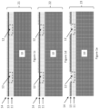
- the first aspect of the present disclosure relates to the manufacture of a plurality of electrodes (15) wherein the electrodes (15) comprise noble metal as exemplified in Figure 1a to 1h , 2a to 2h .
- the method comprises the steps of:
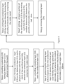
- Figure 4 shows an exemplar flow chart of the main steps of an embodiment of the manufacture method in the present disclosure.
- the masking layer (14) is in physical contact with the conductive layer (13) in step c.
- step g of removing the masking layer (14) is directly after the step f of etching at least a portion of the sacrificial part (12) by dry etching.
- step g of removing the masking layer (14) is after the step e of etching the conductive layer (13) by ion-beam thereby forming the plurality of electrodes (15) and before step f of etching at least a portion of the sacrificial part (12) by dry etching, wherein the dry etching is a non-ion-beam etching.
- the step d of patterning the masking layer (14) to expose at least part of the conductive layer (13) above the sacrificial part (12) defines the edge of the plurality of electrodes (15) such that the smallest distance (d1) between the plurality of electrodes (15) is designed to be not larger than 500nm, preferably not larger than 300nm, more preferably not larger than 200nm, and more preferably not larger than 150nm.
- the masking layer (14) is formed as a conformal layer over the conductive layer (13).
- the sacrificial part (12) consist of the same material as in the dielectric layer (11) thus being part of the dielectric layer (11).
- the conductive layer (13) above and corresponding to the sacrificial part (12) is etched substantially completely by ion-beam thereby forming the plurality of electrodes (15) in step e.
- the present disclosure concerns the manufacture of electrodes comprising at least one type of noble metal.
- An electrode is a conductor through which electric current can pass.
- Noble metals such as gold, platinum, and silver, are often used as electrode materials due to their high conductivity, chemical stability, and resistance to oxidation and corrosion, even in liquid environment. These properties make them ideal for use in a variety of applications, including electrochemical actuator, batteries, and fuel cells.
- the noble metal is selected from the list consisting of platinum (Pt), gold (Au) or silver (Ag). In a preferred embodiment, the noble metal is platinum.
- the substrate (10) is a base material that supports the formation of other layers on top of it.
- the substrate is preferably composed of a semiconductor material, which is a type of material that can conduct electricity under certain conditions.
- the substrate may be a circular wafer or a rectangular wafer die.
- the substrate (10) comprises Silicon (Si), which is the most widely used material for integrated circuits and microelectronics devices. Silicon has high purity, low cost, and excellent electrical and thermal properties.
- the substrate can comprise other semiconductor materials such as Gallium arsenide (GaAs), Sapphire (Al 2 O 3 ), Germanium (Ge).
- the substrate (10) comprises (e.g. consist of) semiconductor material. In some embodiment, the substrate (10) comprises (e.g. consist of) silicon.
- the substrate (10) comprises a stack of semiconductor layers. In some embodiments, the substrate (10) comprises a conductive layer for forming buried conductive connections between electrodes. In some embodiments, the substrate (10) comprises conductive layers and dielectric layers configured for forming switches or other control logic.
- the substrate (10) has a dielectric layer (11) in physical contact therewith.
- a dielectric layer (11) is a layer of material that has a high electrical resistance and can store electric charge. Dielectrics are often used as insulators or capacitors in electronic devices.
- the dielectric layer (11) may comprise any material that can be etched or dissolved by a chemical solution, such as silicon (di)oxide (e.g. SiO 2 ), silicon nitride (Si 3 N 4 ), or polyimide.
- the dielectric layer (11) may have a thickness ranging from 10 nm to 10 ⁇ m.
- the dielectric layer (11) comprises a sacrificial part (12) that has a top surface (121).
- the properties of the dielectric layer (11), such as thickness or material are selected and designed such that the resistance between the electrodes (15) at the smallest distance can reach at least 1e8 ohm.
- the dielectric layer (11) may either be an integral part of the substrate (10) or a separate layer deposited on one of the largest surfaces of the substrate (10) by any suitable method, such as chemical vapor deposition (CVD), physical vapor deposition (PVD), atomic layer deposition (ALD), or spin coating. In either case, the dielectric layer (11) is always in direct contact with the substrate.
- the dielectric layer (11) may have a uniform or non-uniform composition and thickness across the substrate (10).
- the dielectric layer (11) may also have different properties, such as refractive index, dielectric constant, or stress, depending on the application.
- the dielectric layer comprises (e.g. consist of) silicon oxide (e.g. Si x O y , such as SiO 2 ) and/or silicon nitride (e.g. Si x N y , such as Si 3 N 4 ).
- the silicon nitride layer is deposited by chemical vapour deposition (CVD); e.g. plasma-enhanced CVD (PECVD) or low-pressure CVD (LPCVD).
- CVD chemical vapour deposition
- PECVD plasma-enhanced CVD
- LPCVD low-pressure CVD
- the silicon oxide is deposited by chemical vapour deposition (e.g. PECVD or LPCVD) or is formed by thermal oxidation of the Si substrate.
- chemical vapour deposition e.g. PECVD or LPCVD
- thermal oxidation of the Si substrate e.g. PECVD or LPCVD
- the sacrificial part (12) is a portion of the dielectric layer (11) that will be removed in a later step to further enhance the separation between electrodes (15).
- the conductive layer (13) is a layer of electrically conductive material that is deposited on the dielectric layer (11) by any suitable method, such as sputtering, evaporation, electroplating, or electroless plating.
- the conductive layer (13) may have a uniform or non-uniform composition and thickness across the dielectric layer (11).
- the conductive layer (13) comprises at least one type of noble metal.
- the conductive layer (13) may comprise a single material, i.e. a noble metal or alloy thereof, or a combination of materials, such as with different type of noble metals, alloys.
- the conductive layer (13) must comprise a noble metal, such as platinum (Pt), gold (Au), silver (Ag) or palladium (Pd), which has high conductivity, low reactivity, and good compatibility with organic materials.
- the top surface of the substrate (10) can be the top surface of a silicon wafer which is a substantially smooth and flat surface that serves as a base for, e.g. depositing various layers of materials.
- the top surface of the substrate of a wafer may also have different patterns, such as trenches, holes, or pillars, that are formed by lithography and etching processes.
- the top surface of the substrate (10) is planarized by chemical mechanical polishing (CMP) before step b., which involves forming a conductive layer (13) on the dielectric layer (11) and in physical contact with the top surface (121) of the sacrificial part (12), wherein the conductive layer (13) comprises a noble metal.
- CMP chemical mechanical polishing
- the top surface of the conductive layer (13) is planarized by chemical mechanical polishing (CMP) before step c., which involves providing a masking layer (14) in physical contact with the conductive layer (13).
- CMP chemical mechanical polishing
- the masking layer comprises (e.g. consist of) Silicon Oxide (e.g. Si x O y , such as SiO 2 ), silicon nitride (e.g. Si x N y , such as Si 3 N 4 ), Titanium (Ti), Titanium nitride (TiN) and/or diamond like carbon (DLC).
- Silicon Oxide e.g. Si x O y , such as SiO 2
- silicon nitride e.g. Si x N y , such as Si 3 N 4
- Titanium Ti
- TiN Titanium nitride
- DLC diamond like carbon
- the silicon nitride layer is deposited by chemical vapour deposition (e.g. PECVD or LPCVD).
- chemical vapour deposition e.g. PECVD or LPCVD.
- the silicon oxide is deposited by chemical vapour deposition (e.g. PECVD or LPCVD).
- chemical vapour deposition e.g. PECVD or LPCVD.
- the Ti or TiN is deposited by chemical vapour deposition (e.g. PECVD or LPCVD) or atomic layer deposition (ALD).
- chemical vapour deposition e.g. PECVD or LPCVD
- ALD atomic layer deposition
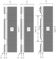
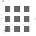
- the second aspect of the present disclosure relates to an electrode array (100), as exemplified in Figure 3 , obtained by the method described in the present disclosure.
- Figure 1h or Figure 2h in the first and second examples of the first aspect can be a zoom-in cross section along the indication line A in Figure 3 .
- the array has a pitch distance (d1) of not larger than 500nm, preferably not larger than 300nm, more preferably not larger than 200nm, and more preferably not larger than 150nm.
- the pitch distance can be measured between a pair of neighboring electrodes, e.g. in the direction of indication line A (d1) or in the direction perpendicular to the indication line A (d1').
- the distance between the pair of neighboring in the direction of indication line A (d1) is substantially equal to the distance between the pair of neighboring in the direction perpendicular to indication line A (d1').
- the array comprises at least a thousand, preferably a million electrodes.
- the third aspect of the present disclosure relates to an electroactive device for bio-material processing comprising:
- the bio-material is biomolecules such as proteins, carbohydrates, lipids, and nucleic acids (e.g. DNA, RNA).
- the bio-material is biologic tissues such as cells and organoids.
- the electroactive device is configured for DNA or RNA synthesis on electrodes.
- the substrate (10) is provided having a dielectric layer (11).
- Sacrificial part (12) is indicated in the dashed square.
- the sacrificial part (12) is an integral part of the dielectric layer (11).
- the top surface of the dielectric layer (11) is planar and the top surface (121) of the sacrificial part (12) is coplanar with a directly surrounding top surface of the dielectric layer (11).
- the top surface of the dielectric layer (11) is planarized by Chemical Mechanical Polishing (CMP) before step b. of forming a conductive layer (13) on the dielectric layer (11) and in physical contact with the top surface (121) of the sacrificial part (12), wherein the conductive layer (13) comprises a noble metal.
- CMP Chemical Mechanical Polishing
- the conductive layer (13) is deposited directly on the dielectric layer (11).
- a stack (20) comprising the substrate (10), the dielectric layer (11), and the conductive layer (13) is formed after step b and before step c.
- the conductive layer (13) completely covers the top surface (121) of the sacrificial part (12), as shown in Figure 1b .
- the conductive layer (13) may have a thickness ranging from 10 nm to 100 nm, preferably from 10 nm to 20 nm.
- the masking layer (14) is deposited directly on the conductive layer.
- a stack (21) comprising the substrate (10), the dielectric layer (11), the conductive layer (13) and the masking layer is formed after step c and before step d.
- the masking layer (14) is provided in physical contact with the conductive layer (13), as shown in Figure 1c .
- the dielectric layer serving as a masking layer (14)
- the masking layer (14) completely covers the conductive layer (13) in the region corresponding to the sacrificial part (12).
- the masking layer (14) can be made of a composite material comprising SiO 2 , Si 3 N 4 , Ti and/or TiN.
- the masking layer (14) can be deposited by any suitable technique, such as chemical vapor deposition (CVD), atomic layer deposition (ALD), physical vapor deposition (PVD), or sputtering.
- the masking layer (14) can have a thickness ranging from 10 nm to 10 ⁇ m, more preferably 5nm to 1 ⁇ m.
- the masking layer (14) is patterned.
- the patterning of the masking layer (14) would expose at least part of the conductive layer to be etched, thereby defining the boundaries of the electrodes.
- a stack (22) comprising the substrate (10), the dielectric layer (11), the conductive layer (13) and a patterned masking layer is formed after step d and before step e.
- the masking layer (14) is patterned to expose at least part of the conductive layer (13) in the regions corresponding to the sacrificial part (12). In an embodiment, the masking layer (14) is patterned to expose at least 70% of the conductive layer (13) in the regions corresponding to the sacrificial part (12). In an embodiment, the masking layer (14) is patterned to expose completely the conductive layer (13) in the regions corresponding to the sacrificial part (12).
- the patterning can be performed by any suitable technique, such as photolithography.
- the exposed part of the conductive layer (13) is etched by ion-beam etching.
- the ion-beam etching is a directional process that can effectively remove the conductive material.
- ion-beam etching uses Ar, Xe, Ne or Kr (i.e. the noble inert gases): this enables physical etching or sputtering and allows, among other processes, etching of noble metals such as Au, Pt, Pd which are non-reactive materials and hence do not respond to reactive plasma or chemical etching.
- the ion-beam etching can have an etching rate ranging from 1 nm/min to 100 nm/min depending on the ion source, the voltage, and the angle of incidence.
- the ion-beam etching can also be controlled by adjusting the duration and the area of exposure.
- the ion-beam etching removes the conductive layer (13) to form electrodes (15) on the dielectric layer (11) in the regions not corresponding to the sacrificial part (12).
- a stack (23) comprising the substrate (10), the dielectric layer (11), a patterned conductive layer (13), i.e. the electrodes (15), and a patterned masking layer (14) is formed after the step e and before step f.
- the dielectric layer (14) serves as a masking layer to protect the conductive layer (13) from being removed in the regions not corresponding to the sacrificial part (12). However, the ion-beam etching will consume part of the masking layer (14). Thus, the masking layer (14) shall have a thickness and characteristics such that it is not completely removed before the conductive layer in the regions corresponding to the sacrificial part (12) is removed. In an embodiment, the masking layer shall have at least a thickness of 25% of the thickness before ion-beam etching. This can ensure that the electrodes (15) are well defined and aligned with the opening (13).
- the masking layer (14) can have a higher etching selectivity than the conductive layer (13), i.e. a lower etching rate, so that it can withstand the ion-beam etching longer than the conductive layer (13).
- the conductive layer corresponding to the sacrificial part (12) is completely removed, ensuring that no electrodes will be formed on top of the sacrificial part (12).
- some noble metal particles are generated from the conductive layer (13) and re-sputtered in the space between the electrodes (15), i.e. above or on the surface of the sacrificial part (12). These noble metal particles can affect the electrical characteristics and performance of the device.
- a cleaning process can be performed to remove the re-sputtered noble metal particles from the space between the electrodes (15) by using a solvent, such as acetone, isopropanol, or ethanol, and applying ultrasonic waves to dissolve and dislodge the noble metal particles.
- a solvent such as acetone, isopropanol, or ethanol
- the solvent can penetrate into the space between the electrodes (15) and the dielectric layer (11), which can cause swelling or cracking of the dielectric layer (11). Moreover, the solvent can also react with the dielectric layer (11) or the electrodes (15), which can degrade their properties or cause corrosion. Furthermore, the ultrasonic waves can generate mechanical stress or vibration on the electrodes (15), which can damage or detach them from the dielectric layer (11). Therefore, the conventional cleaning process using a solvent and ultrasonic wave can compromise the quality and reliability of the device. Furthermore, noble metal, such as Pt, is not removable by standard cleaning solvents. It is typically etched by aggressive solvent such as aqua regia.
- the sacrificial part (12) is etched by dry etching, e.g. reactive ion etching.
- the reactive ion etching can selectively remove the material of the sacrificial part (12) without damaging the electrodes (15).
- the electrodes act as hard mask for reactive ion etching the sacrificial part (12).
- step f of etching is done by a non-ion-beam dry etch so that further re-sputtering of metal particles is prevented.
- part of the sacrificial part (12) is etched by ion-beam etching. Because of the non-ion-beam dry etch, the density of metal particles close to the edge of the electrode is significantly reduced thus increasing the resistance between the electrodes.
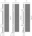
- the resistance at the smallest distance (d1) between the plurality of electrodes (15), as indicated in Figure 1g is at least 1e8 ohm.
- the dry etching can have an etching rate ranging from 10 nm/min to 1000 nm/min depending on the material of the sacrificial part (12), the etching gas, and the etching parameters.
- the dry etching can also be controlled by adjusting the duration and the area of exposure.
- the dry etching removes at least a portion of the sacrificial part (12) to form a cavity that has a depth ranging from 10 nm to 200 nm.
- the dielectric layer (11) comprises recessed regions in the dielectric layer (11), corresponding to the removed sacrificial part, is obtained between the plurality of electrodes (15).
- a stack (24) comprising the substrate (10), the dielectric layer (11) with recessed regions, a patterned conductive layer (13), i.e. the electrodes (15), and a patterned masking layer (14) is formed after the step f and before step g.
- the masking layer (14) is removed by conventional etching methods.
- a stack (25) comprising the substrate (10), the dielectric layer (11) with recessed region and a patterned conductive layer (13), i.e. the electrodes (15) is formed after step f.
- the masking layer (14) can be removed before the reactive ion etching of at least part of the sacrificial part (12).
- the distance (d1) between the electrodes is defined in the step d of patterning the masking layer (14) to expose at least part of the conductive layer (13) above the sacrificial part (12).
- the distance (d2) of the recessed region in the dielectric layer between the electrodes is substantively equal to the distance (d1) between the electrodes. Because, in some embodiments, the electrodes act as hard mask for reactive ion etching the sacrificial part (12).
- the distance (d2) of the recessed region in the dielectric layer between the electrodes within 10% margin of the distance (d1) between the electrodes. In a preferred embodiment, the distance (d2) of the recessed region in the dielectric layer between the electrodes is within 5% margin of the distance (d1) between the electrodes.
- the pitch (d3) is defined after step e of etching the conductive layer (13) by ion-beam thereby forming the plurality of electrodes (15).
- the distance (d1) between the electrodes can be the smallest distance between any two electrodes of the plurality of electrodes.
- the resistance of the said two electrodes which has the smallest distance can be less than 1e8 ohm after dry etching step f.
- the probes of the multimeter or the ohmmeter can be connected to the two electrodes whose resistance is to be measured.
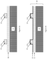
- the substrate (10) is provided having a dielectric layer (11).
- Sacrificial part (12) is indicated in the dashed square.
- the sacrificial part (12) is an integral part of the dielectric layer (11).
- the sacrificial part (12) is a protruded structure (12) of the dielectric layer (11).
- the conductive layer (13) is deposited directly on the dielectric layer (11).
- a stack (20) comprising the substrate (10), the dielectric layer (11), the conductive layer (13) is formed after step b and before step c.
- the conductive layer (13) completely covers the top surface (121) of the sacrificial part (12), as shown in Figure 2b .
- the conductive layer (13) may have a thickness ranging from 10 nm to 100 nm, preferably from 10 nm to 20 nm.
- the masking layer (14) is deposited directly on the conductive layer.
- a stack (21) comprising the substrate (10), the dielectric layer (11), the conductive layer (13) and masking layer is formed after step c and before step d.
- the masking layer (14) is provided in physical contact with the conductive layer (13), as shown in Figure 2c .
- a dielectric layer serving as the masking layer (14), is deposited over the conductive layer (13).
- the masking layer (14) completely covers the conductive layer (13) in the region corresponding to the sacrificial part (12).
- the masking layer (14) can be made of a composite material comprising SiO 2 , Si 3 N 4 , Ti and/or TiN.
- the masking layer (14) can be deposited by any suitable technique, such as chemical vapor deposition (CVD), atomic layer deposition (ALD), physical vapor deposition (PVD), or sputtering.
- the masking layer (14) can have a thickness ranging from 10 nm to 10 ⁇ m, more preferably 5nm to 1 ⁇ m.
- the masking layer (14) is patterned.
- the patterning of the masking layer (14) would expose at least part of conductive layer to be etched thereby defining the boundary of the electrodes.
- a stack (22) comprising the substrate (10), the dielectric layer (11), the conductive layer (13) and a patterned masking layer is formed after step d and before step e.
- the masking layer (14) is patterned to expose at least part of the conductive layer (13) above the protruded structure. In an embodiment, the masking layer (14) is patterned to expose at least 70% of the conductive layer (13) in the regions corresponding to the sacrificial part (12). In an embodiment, the masking layer (14) is patterned to expose completely the conductive layer (13) in the regions corresponding to the sacrificial part (12). The patterning can be performed by any suitable technique, such as photolithography. In an embodiment, the masking layer (14) is patterned to expose completely the conductive layer (13) in the regions corresponding to the sacrificial part (12) and a portion of the masking layer (14) in the neighboring regions of the regions corresponding to the sacrificial part (12).
- the exposed part of the conductive layer (13) is etched by ion-beam etching.
- the ion-beam etching is a directional process that can effectively remove the conductive material.
- ion-beam etching uses Ar, Xe, Ne or Kr (i.e. the noble inert gases): this enables physical etching or sputtering and allows, among other processes, etching of noble metals such as Au, Pt, Pd which are non-reactive materials and hence do not respond to reactive plasma or chemical etching.
- the ion-beam etching can have an etching rate ranging from 1 nm/min to 100 nm/min depending on the ion source, the voltage, and the angle of incidence.
- the ion-beam etching can also be controlled by adjusting the duration and the area of exposure.
- the ion-beam etching removes the conductive layer (13) to form electrodes (15) on the dielectric layer (11) in the regions not corresponding to the sacrificial part (12).
- a stack (23) comprising the substrate (10), the dielectric layer (11), a patterned conductive layer (13), i.e. the electrodes (15), and a patterned masking layer (14) is formed after step e and before step f.
- the masking layer (14) protects the conductive layer (13) from being removed in the regions not corresponding to the sacrificial part (12). However, the ion-beam etching may consume the masking layer (14). Thus, the masking layer (14) shall have a thickness and characteristics such that it is not completely removed before the conductive layer in the regions corresponding to the sacrificial part (12) is removed. In an embodiment, the masking layer shall have at least a thickness of 25% of the thickness before ion-beam etching. This can ensure that the electrodes (15) are well defined and aligned with the opening (13).
- the masking layer (14) can have a higher etching selectivity than the conductive layer (13), i.e. a lower etching rate, so that it can withstand the ion-beam etching longer than the conductive layer (13).
- the conductive layer corresponding to the sacrificial part (12) is completely removed thus no electrode will be formed on top of the sacrificial part (12).
- some noble metal particles are generated from the conductive layer (13) and re-sputtered in the space between the electrodes (15), i.e. above or on the surface of the sacrificial part (12). These noble metal particles can affect the electrical characteristics and performance of the device.
- a cleaning process can be performed to remove the re-sputtered noble metal particles from the space between the electrodes (15) by using a solvent, such as acetone, isopropanol, or ethanol, and applying ultrasonic waves to dissolve and dislodge the noble metal particles.
- a solvent such as acetone, isopropanol, or ethanol
- the solvent can penetrate into the space between the electrodes (15) and the dielectric layer (11), which can cause swelling or cracking of the dielectric layer (11). Moreover, the solvent can also react with the dielectric layer (11) or the electrodes (15), which can degrade their properties or cause corrosion. Furthermore, the ultrasonic waves can generate mechanical stress or vibration on the electrodes (15), which can damage or detach them from the dielectric layer (11). Therefore, the conventional cleaning process using a solvent and ultrasonic wave can compromise the quality and reliability of the device.
- the sacrificial part (12) is etched by dry etching.
- step f of etching can be done by any effective dry etch to remove the sacrificial part. Because of the existence of the protruded structure, the metal particles re-sputtered during the step e mainly lands on the masking layer. Much less of the metal particles would remain in the space between the electrodes.
- the dry etching in step f comprises a continuous ion-beam etching from step e.
- the ion-beam etching initiated in step e continues in step f, thereby constituting the dry etching process for at least a portion of the sacrificial part in step f.
- the resistance at the smallest distance (d1) between the plurality of electrodes (15), as indicated in Figure 1g can be at least 1e8 ohm.
- the dielectric layer (11) comprises regions corresponding to the removed sacrificial part.
- the sacrificial part (12) is further etched by non-ion-beam dry etching, e.g. reactive ion etching.
- the reactive ion etching can selectively remove the material of the sacrificial part (12) without damaging the electrodes (15).
- the electrodes act as hard mask for reactive ion etching the sacrificial part (12).
- a stack (24) comprising the substrate (10), the dielectric layer (11), a patterned conductive layer (13), i.e. the electrodes (15), and a patterned masking layer (14) is formed after the step f and before step g.
- the masking layer (14) is removed by conventional etching methods.
- a stack (25) comprising the substrate (10), the dielectric layer (11) and a patterned conductive layer (13), i.e. the electrodes (15) is formed after step f.
- the masking layer (14) can be removed before the further non-ion-beam dry etching, e.g. reactive ion etching, by conventional etching methods.
- the distance (d1) between the electrodes is defined in the step d of patterning the masking layer (14) to expose at least part of the conductive layer (13) above the sacrificial part (12).
- the pitch (d3) is defined after step e of etching the conductive layer (13) by ion-beam thereby forming the plurality of electrodes (15).
- the distance (d1) between the electrodes can be the smallest distance between any two electrodes of the plurality of electrodes.
- the resistance of the said two electrodes which has the smallest distance can be less than 1e8 ohm after dry etching step f.
- the dry etching in step f comprises a further step of non-ion-beam etching, e.g. reactive ion etching.
- the dry etching can have an etching rate ranging from 10 nm/min to 1000 nm/min depending on the material of the sacrificial part (12), the etching gas, and the etching parameters.
- the dry etching can also be controlled by adjusting the duration and the area of exposure.
- the dry etching removes at least a portion of the sacrificial part (12) to form a cavity (17) that has a depth ranging from 10 nm to 200 nm.
- the dielectric layer (11) comprises recessed regions corresponding to the removed sacrificial part.
- a stack (24) comprising the substrate (10), the dielectric layer (11) with recessed regions, a patterned conductive layer (13), i.e. the electrodes (15), and a patterned masking layer (14) is formed after the step f and before step g.
- the masking layer (14) is removed by conventional etching methods.
- a stack (25) comprising the substrate (10), the dielectric layer (11) with recessed region and a patterned conductive layer (13), i.e. the electrodes (15) is formed after step f.
- the distance (d1) between the electrodes is defined in the step d of patterning the masking layer (14) to expose at least part of the conductive layer (13) above the sacrificial part (12).
- the distance (d2) of the recessed region in the dielectric layer between the electrodes is substantively equal to the distance (d1) between the electrodes.
- the distance (d2) of the recessed region in the dielectric layer between the electrodes is within 10% margin of the distance (d1) between the electrodes.
- the pitch (d3) is defined after step e of etching the conductive layer (13) by ion-beam thereby forming the plurality of electrodes (15).
- the distance (d1) between the electrodes can be the smallest distance between any two electrodes of the plurality of electrodes.
- the resistance of the said two electrodes which has the smallest distance can be less than 1e8 ohm after dry etching step f.
- the probes of the multimeter or the ohmmeter can be connected to the two electrodes whose resistance is to be measured.
Landscapes
- Chemical & Material Sciences (AREA)
- Life Sciences & Earth Sciences (AREA)
- Health & Medical Sciences (AREA)
- Chemical Kinetics & Catalysis (AREA)
- Electrochemistry (AREA)
- Analytical Chemistry (AREA)
- Biochemistry (AREA)
- Pathology (AREA)
- Immunology (AREA)
- General Physics & Mathematics (AREA)
- General Health & Medical Sciences (AREA)
- Physics & Mathematics (AREA)
- Materials Engineering (AREA)
- Engineering & Computer Science (AREA)
- Organic Chemistry (AREA)
- Metallurgy (AREA)
- Molecular Biology (AREA)
- Mechanical Engineering (AREA)
- Micromachines (AREA)
Priority Applications (2)
| Application Number | Priority Date | Filing Date | Title |
|---|---|---|---|
| EP23215275.1A EP4567152A1 (de) | 2023-12-08 | 2023-12-08 | Verfahren zur herstellung von elektroden |
| US18/969,063 US20250189478A1 (en) | 2023-12-08 | 2024-12-04 | Method for manufacturing electrodes |
Applications Claiming Priority (1)
| Application Number | Priority Date | Filing Date | Title |
|---|---|---|---|
| EP23215275.1A EP4567152A1 (de) | 2023-12-08 | 2023-12-08 | Verfahren zur herstellung von elektroden |
Publications (1)
| Publication Number | Publication Date |
|---|---|
| EP4567152A1 true EP4567152A1 (de) | 2025-06-11 |
Family
ID=89164633
Family Applications (1)
| Application Number | Title | Priority Date | Filing Date |
|---|---|---|---|
| EP23215275.1A Pending EP4567152A1 (de) | 2023-12-08 | 2023-12-08 | Verfahren zur herstellung von elektroden |
Country Status (2)
| Country | Link |
|---|---|
| US (1) | US20250189478A1 (de) |
| EP (1) | EP4567152A1 (de) |
Citations (2)
| Publication number | Priority date | Publication date | Assignee | Title |
|---|---|---|---|---|
| WO2009010389A1 (de) * | 2007-07-17 | 2009-01-22 | Robert Bosch Gmbh | Sensorelement zur detektion von leitfähigen partikeln in einem gasstrom sowie verfahren zu dessen herstellung und dessen verwendung |
| US20210288152A1 (en) * | 2017-10-13 | 2021-09-16 | Wayne State University | Method for fabricating wafer scale/nano submicron gap electrodes and arrays via photolithography |
-
2023
- 2023-12-08 EP EP23215275.1A patent/EP4567152A1/de active Pending
-
2024
- 2024-12-04 US US18/969,063 patent/US20250189478A1/en active Pending
Patent Citations (2)
| Publication number | Priority date | Publication date | Assignee | Title |
|---|---|---|---|---|
| WO2009010389A1 (de) * | 2007-07-17 | 2009-01-22 | Robert Bosch Gmbh | Sensorelement zur detektion von leitfähigen partikeln in einem gasstrom sowie verfahren zu dessen herstellung und dessen verwendung |
| US20210288152A1 (en) * | 2017-10-13 | 2021-09-16 | Wayne State University | Method for fabricating wafer scale/nano submicron gap electrodes and arrays via photolithography |
Non-Patent Citations (2)
| Title |
|---|
| HINTSCHE R ET AL: "Microelectrode arrays and application to biosensing devices", BIOSENSORS AND BIOELECTRONICS, ELSEVIER SCIENCE LTD, UK, AMSTERDAM , NL, vol. 9, no. 9-10, 1 January 1994 (1994-01-01), pages 697 - 705, XP026594166, ISSN: 0956-5663, [retrieved on 19940101], DOI: 10.1016/0956-5663(94)80068-5 * |
| YUSUKE SHIOMI ET AL: "High-Yield Bridged Assembly of ssDNA-Modified SWCNT Using Dielectrophoresis", INTERNATIONAL JOURNAL OF AUTOMATION TECHNOLOGY, 5 January 2018 (2018-01-05), pages 29 - 36, XP055740241, Retrieved from the Internet <URL:https://www.fujipress.jp/ijat/au/ijate001200010029/> DOI: 10.20965/ijat.2018.p0029 * |
Also Published As
| Publication number | Publication date |
|---|---|
| US20250189478A1 (en) | 2025-06-12 |
Similar Documents
| Publication | Publication Date | Title |
|---|---|---|
| US7960240B1 (en) | System and method for providing a dual via architecture for thin film resistors | |
| US20170365474A1 (en) | Depositing a passivation layer on a graphene sheet | |
| US8530321B2 (en) | Variable resistance element and manufacturing method thereof | |
| JP2012517105A (ja) | 積層された固体電解質構造を有するプログラマブルメタライゼーションメモリセル | |
| US20160064647A1 (en) | Size-controllable opening and method of making same | |
| US20240395458A1 (en) | Capacitor and method of manufacturing capacitor | |
| SE538018C2 (sv) | Isolering av mikrostrukturer | |
| EP4567152A1 (de) | Verfahren zur herstellung von elektroden | |
| EP2833461B1 (de) | Herstellungsverfahren einer Lithium-Mikrobatterie | |
| CN113145432A (zh) | 电容式超音波换能器及其制造方法 | |
| CN102194614A (zh) | 开关及其制造方法、继电器 | |
| JP2005340398A (ja) | 半導体装置およびその製造方法 | |
| KR100912516B1 (ko) | 다른 요소의 공정 중 메모리 셀의 액티브층 보호 방법 | |
| US11322580B2 (en) | Titanium layer as getter layer for hydrogen in a MIM device | |
| US20140312736A1 (en) | Electricoacoustic Component with Structured Conductor and Dielectric Layer | |
| TW201528492A (zh) | 電阻式記憶體及其製造方法 | |
| CN112104960B (zh) | Mems麦克风器件及其形成方法 | |
| CN119896061A (zh) | 3d nand结构中的字线侧壁接触 | |
| JP5826841B2 (ja) | 直列に接続された複数の基本セルを備える燃料電池及びその製造方法 | |
| US7342314B2 (en) | Device having a useful structure and an auxiliary structure | |
| JP2004140198A (ja) | 半導体装置およびその製造方法 | |
| JP2022524959A (ja) | 積層構造の処理方法 | |
| JPH11251321A (ja) | 集積回路内の電子部品間の導通パス製作方法および集積回路 | |
| JP2014075193A (ja) | 電子装置の製造方法 | |
| JP5743383B2 (ja) | 圧電素子及び圧電装置の製造方法 |
Legal Events
| Date | Code | Title | Description |
|---|---|---|---|
| PUAI | Public reference made under article 153(3) epc to a published international application that has entered the european phase |
Free format text: ORIGINAL CODE: 0009012 |
|
| STAA | Information on the status of an ep patent application or granted ep patent |
Free format text: STATUS: THE APPLICATION HAS BEEN PUBLISHED |
|
| AK | Designated contracting states |
Kind code of ref document: A1 Designated state(s): AL AT BE BG CH CY CZ DE DK EE ES FI FR GB GR HR HU IE IS IT LI LT LU LV MC ME MK MT NL NO PL PT RO RS SE SI SK SM TR |
|
| REG | Reference to a national code |
Ref country code: DE Ref legal event code: R079 Free format text: PREVIOUS MAIN CLASS: C23F0001020000 Ipc: C23F0004040000 |
|
| STAA | Information on the status of an ep patent application or granted ep patent |
Free format text: STATUS: REQUEST FOR EXAMINATION WAS MADE |
|
| GRAP | Despatch of communication of intention to grant a patent |
Free format text: ORIGINAL CODE: EPIDOSNIGR1 |
|
| STAA | Information on the status of an ep patent application or granted ep patent |
Free format text: STATUS: GRANT OF PATENT IS INTENDED |
|
| 17P | Request for examination filed |
Effective date: 20251203 |
|
| RIC1 | Information provided on ipc code assigned before grant |
Ipc: C23F 4/04 20060101AFI20251204BHEP Ipc: C25F 3/14 20060101ALI20251204BHEP Ipc: G01N 27/02 20060101ALI20251204BHEP Ipc: H01L 21/3213 20060101ALI20251204BHEP Ipc: G01N 33/00 20060101ALN20251204BHEP |
|
| INTG | Intention to grant announced |
Effective date: 20251223 |
|
| RAP3 | Party data changed (applicant data changed or rights of an application transferred) |
Owner name: IMEC VZW |
|
| GRAS | Grant fee paid |
Free format text: ORIGINAL CODE: EPIDOSNIGR3 |
|
| GRAA | (expected) grant |
Free format text: ORIGINAL CODE: 0009210 |
|
| STAA | Information on the status of an ep patent application or granted ep patent |
Free format text: STATUS: THE PATENT HAS BEEN GRANTED |