EP4565032A2 - Field effect transistor having loop distributed field effect transistor cells - Google Patents
Field effect transistor having loop distributed field effect transistor cells Download PDFInfo
- Publication number
- EP4565032A2 EP4565032A2 EP25162449.0A EP25162449A EP4565032A2 EP 4565032 A2 EP4565032 A2 EP 4565032A2 EP 25162449 A EP25162449 A EP 25162449A EP 4565032 A2 EP4565032 A2 EP 4565032A2
- Authority
- EP
- European Patent Office
- Prior art keywords
- fet
- gate
- disposed
- substrate
- drain
- Prior art date
- Legal status (The legal status is an assumption and is not a legal conclusion. Google has not performed a legal analysis and makes no representation as to the accuracy of the status listed.)
- Pending
Links
Images





Classifications
-
- H—ELECTRICITY
- H10—SEMICONDUCTOR DEVICES; ELECTRIC SOLID-STATE DEVICES NOT OTHERWISE PROVIDED FOR
- H10D—INORGANIC ELECTRIC SEMICONDUCTOR DEVICES
- H10D84/00—Integrated devices formed in or on semiconductor substrates that comprise only semiconducting layers, e.g. on Si wafers or on GaAs-on-Si wafers
- H10D84/80—Integrated devices formed in or on semiconductor substrates that comprise only semiconducting layers, e.g. on Si wafers or on GaAs-on-Si wafers characterised by the integration of at least one component covered by groups H10D12/00 or H10D30/00, e.g. integration of IGFETs
- H10D84/82—Integrated devices formed in or on semiconductor substrates that comprise only semiconducting layers, e.g. on Si wafers or on GaAs-on-Si wafers characterised by the integration of at least one component covered by groups H10D12/00 or H10D30/00, e.g. integration of IGFETs of only field-effect components
- H10D84/83—Integrated devices formed in or on semiconductor substrates that comprise only semiconducting layers, e.g. on Si wafers or on GaAs-on-Si wafers characterised by the integration of at least one component covered by groups H10D12/00 or H10D30/00, e.g. integration of IGFETs of only field-effect components of only insulated-gate FETs [IGFET]
-
- H—ELECTRICITY
- H10—SEMICONDUCTOR DEVICES; ELECTRIC SOLID-STATE DEVICES NOT OTHERWISE PROVIDED FOR
- H10D—INORGANIC ELECTRIC SEMICONDUCTOR DEVICES
- H10D30/00—Field-effect transistors [FET]
- H10D30/80—FETs having rectifying junction gate electrodes
- H10D30/87—FETs having Schottky gate electrodes, e.g. metal-semiconductor FETs [MESFET]
-
- H—ELECTRICITY
- H10—SEMICONDUCTOR DEVICES; ELECTRIC SOLID-STATE DEVICES NOT OTHERWISE PROVIDED FOR
- H10D—INORGANIC ELECTRIC SEMICONDUCTOR DEVICES
- H10D62/00—Semiconductor bodies, or regions thereof, of devices having potential barriers
- H10D62/10—Shapes, relative sizes or dispositions of the regions of the semiconductor bodies; Shapes of the semiconductor bodies
- H10D62/124—Shapes, relative sizes or dispositions of the regions of semiconductor bodies or of junctions between the regions
- H10D62/126—Top-view geometrical layouts of the regions or the junctions
- H10D62/127—Top-view geometrical layouts of the regions or the junctions of cellular field-effect devices, e.g. multicellular DMOS transistors or IGBTs
-
- H—ELECTRICITY
- H10—SEMICONDUCTOR DEVICES; ELECTRIC SOLID-STATE DEVICES NOT OTHERWISE PROVIDED FOR
- H10D—INORGANIC ELECTRIC SEMICONDUCTOR DEVICES
- H10D64/00—Electrodes of devices having potential barriers
- H10D64/20—Electrodes characterised by their shapes, relative sizes or dispositions
- H10D64/23—Electrodes carrying the current to be rectified, amplified, oscillated or switched, e.g. sources, drains, anodes or cathodes
- H10D64/251—Source or drain electrodes for field-effect devices
- H10D64/257—Source or drain electrodes for field-effect devices for lateral devices wherein the source or drain electrodes are characterised by top-view geometrical layouts, e.g. interdigitated, semi-circular, annular or L-shaped electrodes
-
- H—ELECTRICITY
- H10—SEMICONDUCTOR DEVICES; ELECTRIC SOLID-STATE DEVICES NOT OTHERWISE PROVIDED FOR
- H10D—INORGANIC ELECTRIC SEMICONDUCTOR DEVICES
- H10D64/00—Electrodes of devices having potential barriers
- H10D64/20—Electrodes characterised by their shapes, relative sizes or dispositions
- H10D64/27—Electrodes not carrying the current to be rectified, amplified, oscillated or switched, e.g. gates
- H10D64/311—Gate electrodes for field-effect devices
- H10D64/411—Gate electrodes for field-effect devices for FETs
-
- H—ELECTRICITY
- H10—SEMICONDUCTOR DEVICES; ELECTRIC SOLID-STATE DEVICES NOT OTHERWISE PROVIDED FOR
- H10D—INORGANIC ELECTRIC SEMICONDUCTOR DEVICES
- H10D64/00—Electrodes of devices having potential barriers
- H10D64/20—Electrodes characterised by their shapes, relative sizes or dispositions
- H10D64/27—Electrodes not carrying the current to be rectified, amplified, oscillated or switched, e.g. gates
- H10D64/311—Gate electrodes for field-effect devices
- H10D64/411—Gate electrodes for field-effect devices for FETs
- H10D64/511—Gate electrodes for field-effect devices for FETs for IGFETs
- H10D64/517—Gate electrodes for field-effect devices for FETs for IGFETs characterised by the conducting layers
- H10D64/519—Gate electrodes for field-effect devices for FETs for IGFETs characterised by the conducting layers characterised by their top-view geometrical layouts
-
- H—ELECTRICITY
- H10—SEMICONDUCTOR DEVICES; ELECTRIC SOLID-STATE DEVICES NOT OTHERWISE PROVIDED FOR
- H10W—GENERIC PACKAGES, INTERCONNECTIONS, CONNECTORS OR OTHER CONSTRUCTIONAL DETAILS OF DEVICES COVERED BY CLASS H10
- H10W20/00—Interconnections in chips, wafers or substrates
- H10W20/20—Interconnections within wafers or substrates, e.g. through-silicon vias [TSV]
-
- H—ELECTRICITY
- H10—SEMICONDUCTOR DEVICES; ELECTRIC SOLID-STATE DEVICES NOT OTHERWISE PROVIDED FOR
- H10W—GENERIC PACKAGES, INTERCONNECTIONS, CONNECTORS OR OTHER CONSTRUCTIONAL DETAILS OF DEVICES COVERED BY CLASS H10
- H10W20/00—Interconnections in chips, wafers or substrates
- H10W20/20—Interconnections within wafers or substrates, e.g. through-silicon vias [TSV]
- H10W20/211—Through-semiconductor vias, e.g. TSVs
- H10W20/212—Top-view shapes or dispositions, e.g. top-view layouts of the vias
-
- H—ELECTRICITY
- H10—SEMICONDUCTOR DEVICES; ELECTRIC SOLID-STATE DEVICES NOT OTHERWISE PROVIDED FOR
- H10W—GENERIC PACKAGES, INTERCONNECTIONS, CONNECTORS OR OTHER CONSTRUCTIONAL DETAILS OF DEVICES COVERED BY CLASS H10
- H10W44/00—Electrical arrangements for controlling or matching impedance
- H10W44/20—Electrical arrangements for controlling or matching impedance at high-frequency [HF] or radio frequency [RF]
-
- H—ELECTRICITY
- H10—SEMICONDUCTOR DEVICES; ELECTRIC SOLID-STATE DEVICES NOT OTHERWISE PROVIDED FOR
- H10D—INORGANIC ELECTRIC SEMICONDUCTOR DEVICES
- H10D62/00—Semiconductor bodies, or regions thereof, of devices having potential barriers
- H10D62/80—Semiconductor bodies, or regions thereof, of devices having potential barriers characterised by the materials
- H10D62/85—Semiconductor bodies, or regions thereof, of devices having potential barriers characterised by the materials being Group III-V materials, e.g. GaAs
- H10D62/8503—Nitride Group III-V materials, e.g. AlN or GaN
-
- H—ELECTRICITY
- H10—SEMICONDUCTOR DEVICES; ELECTRIC SOLID-STATE DEVICES NOT OTHERWISE PROVIDED FOR
- H10W—GENERIC PACKAGES, INTERCONNECTIONS, CONNECTORS OR OTHER CONSTRUCTIONAL DETAILS OF DEVICES COVERED BY CLASS H10
- H10W44/00—Electrical arrangements for controlling or matching impedance
- H10W44/20—Electrical arrangements for controlling or matching impedance at high-frequency [HF] or radio frequency [RF]
- H10W44/203—Electrical connections
- H10W44/209—Vertical interconnections, e.g. vias
- H10W44/212—Coaxial feed-throughs in substrates
-
- H—ELECTRICITY
- H10—SEMICONDUCTOR DEVICES; ELECTRIC SOLID-STATE DEVICES NOT OTHERWISE PROVIDED FOR
- H10W—GENERIC PACKAGES, INTERCONNECTIONS, CONNECTORS OR OTHER CONSTRUCTIONAL DETAILS OF DEVICES COVERED BY CLASS H10
- H10W44/00—Electrical arrangements for controlling or matching impedance
- H10W44/20—Electrical arrangements for controlling or matching impedance at high-frequency [HF] or radio frequency [RF]
- H10W44/203—Electrical connections
- H10W44/216—Waveguides, e.g. strip lines
Definitions
- This disclosure relates generally to Field Effect Transistors (FETs) and more particularly to improved layouts for such FETs.
- FETs Field Effect Transistors having a linear array of a plurality of FET cells are used in many applications.
- Each one of the FET cells has a source, a drain and a gate between the source and the drain to control a flow of carriers along a channel between the source and drain.
- the source and drain may be reversed in any electrical circuit application; with, in either circuit application, the gate controlling the flow of carriers between a source and a drain.
- the gates are finger-like gates interconnected to a common gate contact on the top surface of a substrate.
- the individual drains connected to a common drain contact electrode and the sources are connected to a common source contact using air bridges over the gate fingers and over either the drains, or over the sources, and with air bridges connected to a common drain, or source, contact on the bottom surface of the substrate.
- a FET with the air bridges over the drains is shown in FIG. 1 .
- many of these are FET cells are stacked together in a linear array in the output stage of a power amp Monolithic Microwave Integrated Circuit (MMIC), as shown in FIG. 1 . The linear stacking of these FET cells determines the linear dimension size of the MMIC.
- MMIC Monolithic Microwave Integrated Circuit
- a Field Effect Transistor having: a plurality of FET cells having a plurality of source pads, a plurality of drain pads, and a plurality of gate electrodes disposed on a surface of a substrate; each one of the FET cells having a corresponding one of the gate electrodes disposed between one of the source pads and one of the drain pads; a drain contact connected to the drain pad of each one of the FET cells; and a source contact connected to source pad of each one of the FET cells.
- the cells are disposed in a loop configuration.
- the FET gate contact is disposed on a bottom surface of the substrate and an electrically conductive gate via passes through the substrate to electrically connect the gate contact to the gate pad.
- the gate pad is disposed in an inner region of the loop.
- the gate projects outwardly from the gate pad.
- the drain contact is disposed on the upper surface of the substrate.
- the source contact is a conductor disposed on the bottom surface of the substrate and is connected to the source pad of each one of the FET cells though a corresponding one of a plurality of electrically conductive source vias passing through the substrate.
- a strip conductor is disposed on the bottom of the substrate, the feed line having one end connected to the gate contact, the feed line being spaced from the conductor disposed on the bottom surface of the substrate and connected to the gate contact through a gate via passing through the substrate.
- the strip conductor and the conductor disposed on the bottom surface of the substrate provide a coplanar waveguide transmission line
- the gate via and the plurality of source vias provide a quasi-coaxial transmission line.
- the loop configuration is a circle.
- a Field Effect Transistor (FET) 10 is shown here formed using photo-lithographic chemical etching processing. More particularly, the FET 10 includes a plurality of, here eight, FET cells 12 1 -12 8 , ( FIG. 3A ) interconnected by eight air bridges 11 1 -11 8 and controlled by a corresponding one of eight gates G 1 -G 8 , respectively ( FIGS. 2 and 3A ; FIG. 3B showing the FET 10 with the air bridges 11 1 -11 8 removed to more clearly show the cells 12 1 -12 8 ).
- Each one of the FET cells 12 1 -12 8 has, on an upper, planar surface 13 of a semiconductor substrate 15, here for example a substrate having gallium nitride (GaN), a corresponding one of eight gates G 1 -G 8 , respectively, in Schottky contact with the surface 13 of the semiconductor substrate 15, as shown in FIG. 1 ; each one of the eight gates G 1 -G 8 being disposed between a source (S) and a drain (D) in a manner to be described in more detail hereinafter to control a flow of carriers along a channel between the source pad (S) and drain pad (D) of each one of the eight, FET cells 12 1 -12 8 .
- a semiconductor substrate 15 here for example a substrate having gallium nitride (GaN), a corresponding one of eight gates G 1 -G 8 , respectively, in Schottky contact with the surface 13 of the semiconductor substrate 15, as shown in FIG. 1 ; each one of the eight gates G 1 -G 8 being disposed between
- each one of the gates G 1 -G 8 is here an elongated, finger-like gate and extends radially outward from a central, circular shaped gate pad 17, as shown.
- the gate pad 17 is electrically connected to a gate contact 18, shown more clearly in FIG. 4 ) disposed on a bottom surface 19 (FIG. 2B) of the semiconductor substrate 17 through an electrically conductive gate via 21 disposed at the center of the gate pad 17 and passing vertically through the substrate 15 between the gate pad 17 and the gate contact 23 ( FIGS. 3C and 4 ).
- the elongated, finger-like gates G 1 -G 8 are regularly spaced about the outer periphery of the common gate pad 17.
- the finger-like gate electrodes G 1 -G 8 are electrically interconnected to successive, evenly spaced points, P, ( FIG. 3B ) along an outer edge of the common, circular shaped, gate pad 17.
- P points
- the here eight elongated, finger-like gates Gi-Gs are separated one from the other by here forty-five degrees.
- the FET 10 also includes a drain contact 16 disposed on the upper surface 13 of the substrate 15 and terminating in a circular ring-like structure 18 ( FIG. 4 ) having a plurality of, here four, radially inwardly extending projections 20 1 -20 4 regularly spaced about an outer, circumferential rim of the circular structure 18; each one of the projections 20 1 -20 4 is a drain pad in ohmic contacted with the surface 13 of the semiconductor substrate 15.
- Each one of the projections 20 1 -20 8 provides a drain (D) ( FIGS. 2 , 3A , 3B ) for a pair of adjacent FET cells 12 1 -12 8 , in a manner to be described in more detail hereinafter.
- the central axis of the circular structure 18 and the center of the circular, common pad 17 are co-axial and are disposed along a common vertical Z axis, such Z axis being perpendicular to the X-Y planar surface 13 ( FIG. 3B ).
- the surface 13 is in the X-Y plane and the common vertical axis is along the Z-axis.
- the projections 20 1 -20 4 are spaced one from another by ninety degrees. It is noted that the projections 20 1 -20 4 terminate a predetermined distance from the outer periphery of the common gate pad 17 ( FIG. 3B ).
- each one of the projections 20 1 -20 4 is disposed between every other adjacent pair of the finger-like gates G 1 -G 8 ; as shown most clearly in FIG. 3B .
- each one of the projections 20 1 - 20 4 provides two drains (D) for the FET 10, one radial positioned side region of the projection 20 1 - 20 4 providing a drain for one of the eight FET cells 12 1 -12 8 and the opposite radially positioned side region providing a drain for the adjacent one of the eight FET cells 12 1 -12 8 .
- projection 20 1 is disposed between gates G 2 and G 3 ; projection 20 2 is disposed between gates G 4 and G 5 ; projection 20 3 is disposed between gates G 6 and G 7 ; and projection 20 4 is disposed between gates G 8 and G 1 .
- one side region of projection 20 1 provides the drain for FET cell 12 2 while the opposite side region of projection 20 1 provides the drain for FET cell 12 3 ;
- one side region of projection 20 2 provides the drain for FET cell 12 4 while the opposite side region of projection 20 1 provides the drain for FET cell 12 5 ;
- one side region of projection 20 3 provides the drain for FET cell 12 6 while the opposite side region of projection 20 3 provides the drain for FET cell 12 7 ;
- one side region of projection 20 4 provides the drain for FET cell 18 2 while the opposite side region of projection 20 4 provides the drain for FET cell 12 1 .
- An annular structure 30 ( FIG. 4 ) having a center coaxial with both the gate pad 17 and the circular ring-like structure 18 (along the Z-axis) has four source pads 22 1 - 22 4 ( FIGS. 2 , 3A and 3B ) regularly spaced circumferentially about the annular structure 30; that is the source pads 22 1 - 22 4 are spaced one from the other by ninety degrees and are disposed on the upper surface 13 ( FIGS. 2 , 3A and 3B ). Each one of the source pads 22 1 - 22 4 is in ohmic contacted with the surface 13 of the semiconductor substrate 15.
- the source pads 22 1 - 22 4 ( FIG. 4 ) are electrically interconnected by the air bridges 11 1 -11 4 ( FIGS.
- each one of the air bridges 11 1 -11 4 is elevated from the surface 13 and, more particularly, each one of the air bridges 11 1 -11 4 is elevated from a corresponding one of the projections 20 1 -20 4 and over a pair of adj acent Gi-Gs on each side of the such corresponding one of the projections; one gate finger on either side of the projection 20 1 -20 4 .
- air bridge 11 1 is over projection 20 1 and over gate fingers G 2 and G 3 ; air bridge 11 2 is over projection 20 2 and over gate fingers G 4 and G 5 ; air bridge 11 3 is over projection 20 3 and over gate fingers G 6 and G 7 ; and air bridge 11 4 is over projection 20 4 and over gate fingers G 8 and G 1 ; as indicated in FIGS. 2 and 3B .
- each one of the four source pads 22 1 - 22 4 is disposed between an adjacent pair of the finger-like gates G 1 -G 8 .
- source pad 22 1 is disposed between gates G 1 and G 2 ; source pad 22 2 is disposed between gates G 3 and G 4 ; source pad 22 3 is disposed between gates G 5 and G 6 ; and source pad 22 4 is disposed between gates G 7 and G 8 as shown in FIG. 3B .
- each one of the source pads 22 1 - 22 4 provides two sources (S) for the FET 10, one radial positioned side region of the source pad 22 1 - 22 4 providing a source (S) for one of the eight FET cells 12 1 -12s and the opposite radially positioned side region providing a source (S) for the adjacent one of the eight FET cells 12 1 -12 8 .
- each one of the gate fingers G 1 -G 8 is disposed between a source (S) and drain (D), with each one of the fingers Gi-Gs being adjacent one side of one of the source (S) and one side of the drain (D) while an adjacent one of the gate fingers G 1 -G 8 is adjacent the other side of the same drain (D) and one of the source (S). It follows then that each gate finger (G) shares a drain (D) provided by one of the projections or drain pads 20 1 -20 4 and a source (S) provided by an adjacent one of the source pads22 1 - 22 4 .
- a source contact 25, here provided by an electrical conductor 25 on the bottom surface 19 of the substrate 17 is electrically connected to the sources pads 22 1 -22 4 of the FET cells 12 1 -14 8 through, here four vias 27 ( FIGS. 2 , 3A and 4 ) passing vertically through the substrate 15 between the conductor 25 and the four source pads 22 1 -22 4 .
- a conductive feed 32 ( FIG. 4 ) for the gate pad 17.
- the feed 32 is a strip conductor 34 terminating in the gate contact 23.
- the gate contact 23 is connected to the gate pad 17 with a gate via 21.
- the gate via 21 is disposed within a circular array of the vias 27 thus forming a vertical quasi coaxial transmission line.
- the electrical conductor 25 ( FIG. 4 ) and feed 32 are electrically insulated from each other by the portion of the substrate 19 in the space between the feed 32 and the electrical conductor 25, as indicated.
- the conductor 25 on the bottom of the substrate 15 is spaced a predetermined distance from the feed line 34, as indicated, to provide a coplanar waveguide (CPW) transmission line feed for the 32.
- CPW coplanar waveguide
- the FET cells 12 1 -12 8 are disposed in an X-Y plane in a closed loop configuration, here for example, a circular configuration in the X-Y plane ( Fig. 3A and 3B ) on the upper surface 13 of the substrate 19.
- the FET 10 is suitable for flip chip mounting to a printed circuit board.
- the FET 10' has the air bridges 11 1 -11 4 eliminated since each one of the source pads 22 1 -22 4 is connected to ground conductor 25 of the bottom of the substrate 15 with the vias 27. More particularly, it was recognized that because the gates G1-G8 extend radially out from the pad 17, the source pads 22 1 -22 4 are triangular shaped and thus flare out from the center of the pad 17, there is now sufficient space towards the base of the triangle for placement of a via 27 thus eliminating the need for air bridges. To put it another way, the gate to gate spacing spreads out as one moves away from the center of the FET which allows for vias 27 for each source pad without growing the size of the FET.
- the FET 10' again includes the plurality of, here eight, FET cells 12 1 -12 8 , ( FIG. 3A ); here, however they are interconnected by the electrical conductor 25 through the vias 27. More particularly, as described above and shown more clearly in FIG 3B , one side region of projection 20 1 provides the drain for FET cell 12 2 while the opposite side region of projection 20 1 provides the drain for FET cell 12 3 ; one side region of projection 20 2 provides the drain for FET cell 12 4 while the opposite side region of projection 20 1 provides the drain for FET cell 12 5 ; one side region of projection 20 3 provides the drain for FET cell 12 6 while the opposite side region of projection 20 3 provides the drain for FET cell 12 7 ; and one side region of projection 20 4 provides the drain for FET cell 18 2 while the opposite side region of projection 20 4 provides the drain for FET cell 12 1 .
- the drain / RF output can be bonded to from the topside of this circular FET as shown in FIG. 5A .
- the FET 10' mounted to a printed circuit board 30 having an input impedance matching network (IMN) and an output impedance matching network (OMN) coupled to the FET 10'.
- the IMN is coupled to the gate contact 23 through a microstrip transmission line having a strip conductor 36 separated from a ground plane conductor 38.
- the strip conductor 36 is connected to the strip conductor 34 ( FIG. 4 ).
- the OMN is coupled to the drain contact 16 through a conductor 38 connecting the strip conductor 40 of a microstrip transmission line separated from an underlying portion of the ground plane conductor 38.
- a Field Effect Transistor includes: a plurality of FET cells having a plurality of source pads, a plurality of drain pads, and a plurality of gate electrodes disposed on a surface of a substrate, each one of the FET cells having a corresponding one of the gate electrodes disposed between one of the source pads and one of the drain pads, a gate contact connected to the gate electrode of each one of the FET cells, a drain contact connected to the drain pad of each one of the FET cells and a source contact connected to source pad of each one of the FET cells; wherein the cells are disposed in a loop configuration.
- the FET may include one or more of the following features, independently or in combination with another feature, to include: a gate pad disposed on an upper surface of the substrate connected to the plurality of gate electrodes wherein the gate contact is disposed on an bottom surface of the substrate; and wherein an electrically conductive gate via passes through the substrate to electrically connect the gate contact to the gate pad; wherein the gate pad is disposed in an inner region of the loop; wherein the gate electrodes projects outwardly from the gate pad; wherein one of the source contact or the drain contact is disposed on the bottom surface of the substrate; wherein one of the source contact or the drain contact is a conductor disposed on the bottom surface of the substrate and is connected to the corresponding one of the source pad or drain pad of each one of the FET cells though a corresponding one of a plurality of electrically conductive vias passing through the substrate; a strip conductor disposed on the bottom of the substrate, the feed line having one end connected to the gate contact through a gate via passing through the substrate, the feed line being spaced from
- a Field Effect Transistor includes: a plurality of FET cells having a plurality of source pads, a plurality of drain pads, and a plurality of gate electrodes disposed on a surface of a substrate; each one of the FET cells having a corresponding one of the gate electrodes disposed between one of the source pads and one of the drain pads; a gate contact connected to the gate electrodes of each one of the FET cells; a drain contact connected to the drain pad of each one of the FET cells; and a source contact connected to source pad of each one of the FET cells wherein the gate electrode of each one of the plurality of FET cells projects radially outwardly from a center of the FET.
- the FET may include one or more of the following features, independently or in combination with another feature, to include: wherein one of the source pads or drain pads of each one of the FET cells in the plurality of FET cells is connected to a contact on a bottom surface of the substrate through a corresponding one of a plurality of vias passing through the substrate, and wherein each one of the plurality of vias is disposed between a pair of the gates; a strip conductor disposed on the bottom of the substrate, the feed line having one end connected to the gate contact through a gate via passing through the substrate, the feed line being spaced from the conductor disposed on the bottom surface of the substrate; wherein the strip conductor and the conductor disposed on the bottom surface of the substrate provide a coplanar waveguide transmission line; wherein the gate via and the plurality of vias provide a quasi-coaxial transmission line.
Landscapes
- Junction Field-Effect Transistors (AREA)
Abstract
Description
- This disclosure relates generally to Field Effect Transistors (FETs) and more particularly to improved layouts for such FETs.
- As is known in the art, Field Effect Transistors (FETs) having a linear array of a plurality of FET cells are used in many applications. Each one of the FET cells has a source, a drain and a gate between the source and the drain to control a flow of carriers along a channel between the source and drain. It should also be understood the source and drain may be reversed in any electrical circuit application; with, in either circuit application, the gate controlling the flow of carriers between a source and a drain.
- As is also known in the art, in some FETs, the gates are finger-like gates interconnected to a common gate contact on the top surface of a substrate. Likewise, the individual drains connected to a common drain contact electrode and the sources are connected to a common source contact using air bridges over the gate fingers and over either the drains, or over the sources, and with air bridges connected to a common drain, or source, contact on the bottom surface of the substrate. A FET with the air bridges over the drains is shown in
FIG. 1 . Generally, many of these are FET cells are stacked together in a linear array in the output stage of a power amp Monolithic Microwave Integrated Circuit (MMIC), as shown inFIG. 1 . The linear stacking of these FET cells determines the linear dimension size of the MMIC. SUMMARY - In accordance with the present disclosure, a Field Effect Transistor (FET) is provided having: a plurality of FET cells having a plurality of source pads, a plurality of drain pads, and a plurality of gate electrodes disposed on a surface of a substrate; each one of the FET cells having a corresponding one of the gate electrodes disposed between one of the source pads and one of the drain pads; a drain contact connected to the drain pad of each one of the FET cells; and a source contact connected to source pad of each one of the FET cells. The cells are disposed in a loop configuration.
- In one embodiment, the FET gate contact is disposed on a bottom surface of the substrate and an electrically conductive gate via passes through the substrate to electrically connect the gate contact to the gate pad.
- In one embodiment, the gate pad is disposed in an inner region of the loop.
- In one embodiment, the gate projects outwardly from the gate pad.
- In one embodiment, the drain contact is disposed on the upper surface of the substrate.
- In one embodiment, the source contact is a conductor disposed on the bottom surface of the substrate and is connected to the source pad of each one of the FET cells though a corresponding one of a plurality of electrically conductive source vias passing through the substrate.
- In one embodiment, a strip conductor is disposed on the bottom of the substrate, the feed line having one end connected to the gate contact, the feed line being spaced from the conductor disposed on the bottom surface of the substrate and connected to the gate contact through a gate via passing through the substrate.
- In one embodiment, the strip conductor and the conductor disposed on the bottom surface of the substrate provide a coplanar waveguide transmission line
- In one embodiment, the gate via and the plurality of source vias provide a quasi-coaxial transmission line.
- In one embodiment, the loop configuration is a circle.
- The details of one or more embodiments of the disclosure are set forth in the accompanying drawings and the description below. Other features, objects, and advantages of the disclosure will be apparent from the description and drawings, and from the claims.
-
-
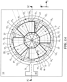
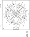
FIG. 1 is a plan view of a Field Effect Transistor (FET) having a plurality of interconnected FET cells according to the PRIOR ART; -
FIG. 2 is a perspective view of a Field Effect Transistor (FET) having a plurality of interconnected FET cells according to the disclosure; -
FIG. 3A is a plan view of the FET ofFIG. 2 ; -
FIG. 3B is a plan view of the FET ofFIG. 3A with air bridges used in the FET ofFIG. 2 removed to more clearly show elements of the FET ofFIG. 2 covered by the air bridges; -
FIG. 3C is a cross sectional view of a portion of the FET ofFIG. 2 , such cross section being taken alongline 3C-3C ofFIG. 3A ; -
FIG. 3D is a cross sectional view of a portion of the FET ofFIG. 2 , such cross section being taken alongline 3C-3C ofFIG. 3A ; -
FIG. 4 is an exploded perspective view of the FET ofFIG. 2 ; and -
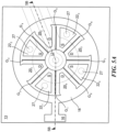
FIG. 5 is a perspective view of a FET having a plurality of interconnected FET cells according to another embodiment of the disclosure; -
FIG, 5A is a plane view of the FET ofFIG. 5 ; and -
FIG. 5B is a cross sectional view of the FET ofFIG. 5 , such cross section being taken alongline 5B-5B ofFIG. 5A with the FET mounted to a printed circuit board having an input impedance matching network (IMN) and an output impedance matching network (OMN) coupled to the FET. - Like reference symbols in the various drawings indicate like elements.
- Referring now to
FIG. 2 ,3A ,3B ,3C ,3D and4 , a Field Effect Transistor (FET) 10 is shown here formed using photo-lithographic chemical etching processing. More particularly, theFET 10 includes a plurality of, here eight, FET cells 121-128, (FIG. 3A ) interconnected by eight air bridges 111-118 and controlled by a corresponding one of eight gates G1-G8, respectively (FIGS. 2 and3A ;FIG. 3B showing theFET 10 with the air bridges 111-118 removed to more clearly show the cells 121-128). Each one of the FET cells 121-128 has, on an upper,planar surface 13 of asemiconductor substrate 15, here for example a substrate having gallium nitride (GaN), a corresponding one of eight gates G1-G8, respectively, in Schottky contact with thesurface 13 of thesemiconductor substrate 15, as shown inFIG. 1 ; each one of the eight gates G1-G8 being disposed between a source (S) and a drain (D) in a manner to be described in more detail hereinafter to control a flow of carriers along a channel between the source pad (S) and drain pad (D) of each one of the eight, FET cells 121-128. Suffice it to say here; however that each one of the gates G1-G8 is here an elongated, finger-like gate and extends radially outward from a central, circularshaped gate pad 17, as shown. Thegate pad 17 is electrically connected to agate contact 18, shown more clearly inFIG. 4 ) disposed on a bottom surface 19 (FIG. 2B) of thesemiconductor substrate 17 through an electrically conductive gate via 21 disposed at the center of thegate pad 17 and passing vertically through thesubstrate 15 between thegate pad 17 and the gate contact 23 (FIGS. 3C and4 ). The elongated, finger-like gates G1-G8 are regularly spaced about the outer periphery of thecommon gate pad 17. More particularly, the finger-like gate electrodes G1-G8 are electrically interconnected to successive, evenly spaced points, P, (FIG. 3B ) along an outer edge of the common, circular shaped,gate pad 17. Thus, the here eight elongated, finger-like gates Gi-Gs are separated one from the other by here forty-five degrees. - The FET 10 also includes a
drain contact 16 disposed on theupper surface 13 of thesubstrate 15 and terminating in a circular ring-like structure 18 (FIG. 4 ) having a plurality of, here four, radially inwardly extending projections 201-204 regularly spaced about an outer, circumferential rim of thecircular structure 18; each one of the projections 201-204 is a drain pad in ohmic contacted with thesurface 13 of thesemiconductor substrate 15. Each one of the projections 201-208 provides a drain (D) (FIGS. 2 ,3A ,3B ) for a pair of adjacent FET cells 121-128, in a manner to be described in more detail hereinafter. The central axis of thecircular structure 18 and the center of the circular,common pad 17 are co-axial and are disposed along a common vertical Z axis, such Z axis being perpendicular to the X-Y planar surface 13 (FIG. 3B ). Thus, here thesurface 13 is in the X-Y plane and the common vertical axis is along the Z-axis. Thus, here the projections 201-204 are spaced one from another by ninety degrees. It is noted that the projections 201-204 terminate a predetermined distance from the outer periphery of the common gate pad 17 (FIG. 3B ). It is also noted that each one of the projections 201-204 is disposed between every other adjacent pair of the finger-like gates G1-G8; as shown most clearly inFIG. 3B . Thus, each one of the projections 201 - 204 provides two drains (D) for theFET 10, one radial positioned side region of the projection 201- 204 providing a drain for one of the eight FET cells 121-128 and the opposite radially positioned side region providing a drain for the adjacent one of the eight FET cells 121-128. Thus, here,projection 201 is disposed between gates G2 and G3;projection 202 is disposed between gates G4 and G5;projection 203 is disposed between gates G6 and G7; andprojection 204 is disposed between gates G8 and G1. More particularly, looking vertically downward on theFET 10 and progressing clockwise; one side region ofprojection 201 provides the drain forFET cell 122 while the opposite side region ofprojection 201 provides the drain forFET cell 123; one side region ofprojection 202 provides the drain forFET cell 124 while the opposite side region ofprojection 201 provides the drain forFET cell 125; one side region ofprojection 203 provides the drain forFET cell 126 while the opposite side region ofprojection 203 provides the drain forFET cell 127; and one side region ofprojection 204 provides the drain forFET cell 182 while the opposite side region ofprojection 204 provides the drain forFET cell 121. - An annular structure 30 (
FIG. 4 ) having a center coaxial with both thegate pad 17 and the circular ring-like structure 18 (along the Z-axis) has four source pads 221- 224 (FIGS. 2 ,3A and3B ) regularly spaced circumferentially about theannular structure 30; that is the source pads 221 - 224 are spaced one from the other by ninety degrees and are disposed on the upper surface 13 (FIGS. 2 ,3A and3B ). Each one of the source pads 221 - 224 is in ohmic contacted with thesurface 13 of thesemiconductor substrate 15. The source pads 221- 224 (FIG. 4 ) are electrically interconnected by the air bridges 111-114 (FIGS. 2 ,3A and4 ; the air bridges 111-114 not being shown inFIG. 3B as mentioned above). Thus, the each one of the air bridges 111-114 is elevated from thesurface 13 and, more particularly, each one of the air bridges 111-114 is elevated from a corresponding one of the projections 201-204 and over a pair of adj acent Gi-Gs on each side of the such corresponding one of the projections; one gate finger on either side of the projection 201-204. Thus,air bridge 111 is overprojection 201 and over gate fingers G2 and G3;air bridge 112 is overprojection 202 and over gate fingers G4 and G5;air bridge 113 is overprojection 203 and over gate fingers G6 and G7; andair bridge 114 is overprojection 204 and over gate fingers G8 and G1; as indicated inFIGS. 2 and3B . Thus, it is noted that each one of the four source pads 221- 224 is disposed between an adjacent pair of the finger-like gates G1-G8. Thus,source pad 221 is disposed between gates G1 and G2;source pad 222 is disposed between gates G3 and G4;source pad 223 is disposed between gates G5 and G6; andsource pad 224 is disposed between gates G7 and G8 as shown inFIG. 3B . Thus, each one of the source pads 221- 224 provides two sources (S) for theFET 10, one radial positioned side region of the source pad 221 - 224 providing a source (S) for one of the eight FET cells 121-12s and the opposite radially positioned side region providing a source (S) for the adjacent one of the eight FET cells 121-128. Thus, each one of the gate fingers G1-G8 is disposed between a source (S) and drain (D), with each one of the fingers Gi-Gs being adjacent one side of one of the source (S) and one side of the drain (D) while an adjacent one of the gate fingers G1-G8 is adjacent the other side of the same drain (D) and one of the source (S). It follows then that each gate finger (G) shares a drain (D) provided by one of the projections or drain pads 201-204 and a source (S) provided by an adjacent one of the source pads221 - 224. - Referring again to
FIG. 4 , asource contact 25, here provided by anelectrical conductor 25 on thebottom surface 19 of thesubstrate 17 is electrically connected to the sources pads 221-224 of the FET cells 121-148 through, here four vias 27 (FIGS. 2 ,3A and4 ) passing vertically through thesubstrate 15 between theconductor 25 and the four source pads 221-224. Also formed on thebottom surface 19 of thesubstrate 15 is a conductive feed 32 (FIG. 4 ) for thegate pad 17. Thefeed 32 is astrip conductor 34 terminating in thegate contact 23. Thegate contact 23 is connected to thegate pad 17 with a gate via 21. It is noted that the gate via 21 is disposed within a circular array of the vias 27 thus forming a vertical quasi coaxial transmission line. It is also noted that the electrical conductor 25 (FIG. 4 ) and feed 32 are electrically insulated from each other by the portion of thesubstrate 19 in the space between thefeed 32 and theelectrical conductor 25, as indicated. Thus, theconductor 25 on the bottom of thesubstrate 15 is spaced a predetermined distance from thefeed line 34, as indicated, to provide a coplanar waveguide (CPW) transmission line feed for the 32. Thus, an RF input signal is fed to theFET 10 through the backside in a quasi-coax approach. - Thus, the FET cells 121-128 are disposed in an X-Y plane in a closed loop configuration, here for example, a circular configuration in the X-Y plane (
Fig. 3A and3B ) on theupper surface 13 of thesubstrate 19. TheFET 10 is suitable for flip chip mounting to a printed circuit board. - Referring now to
FIG. 5 , here the FET 10' has the air bridges 111-114 eliminated since each one of the source pads 221-224 is connected to groundconductor 25 of the bottom of thesubstrate 15 with thevias 27. More particularly, it was recognized that because the gates G1-G8 extend radially out from thepad 17, the source pads 221-224 are triangular shaped and thus flare out from the center of thepad 17, there is now sufficient space towards the base of the triangle for placement of a via 27 thus eliminating the need for air bridges. To put it another way, the gate to gate spacing spreads out as one moves away from the center of the FET which allows forvias 27 for each source pad without growing the size of the FET. - Thus, here the FET 10' again includes the plurality of, here eight, FET cells 121-128, (
FIG. 3A ); here, however they are interconnected by theelectrical conductor 25 through thevias 27. More particularly, as described above and shown more clearly inFIG 3B , one side region ofprojection 201 provides the drain forFET cell 122 while the opposite side region ofprojection 201 provides the drain forFET cell 123; one side region ofprojection 202 provides the drain forFET cell 124 while the opposite side region ofprojection 201 provides the drain forFET cell 125; one side region ofprojection 203 provides the drain forFET cell 126 while the opposite side region ofprojection 203 provides the drain forFET cell 127; and one side region ofprojection 204 provides the drain forFET cell 182 while the opposite side region ofprojection 204 provides the drain forFET cell 121. - The drain / RF output can be bonded to from the topside of this circular FET as shown in
FIG. 5A . Thus, referring toFIG. 5B the FET 10' mounted to a printedcircuit board 30 having an input impedance matching network (IMN) and an output impedance matching network (OMN) coupled to the FET 10'. More particularly, the IMN is coupled to thegate contact 23 through a microstrip transmission line having astrip conductor 36 separated from aground plane conductor 38. More particularly, thestrip conductor 36 is connected to the strip conductor 34 (FIG. 4 ). The OMN is coupled to thedrain contact 16 through aconductor 38 connecting thestrip conductor 40 of a microstrip transmission line separated from an underlying portion of theground plane conductor 38. - A number of embodiments of the disclosure have been described. Nevertheless, it will be understood that various modifications may be made without departing from the spirit and scope of the disclosure. For example, other loop configurations may be used such as, for example, an oval or square or rectangular or triangular or other polygon shaped configuration. Further, the source and drain may be reversed in any electrical circuit application; with, in either circuit application, the gate controlling the flow of carriers between a source and a drain.
- It should now be appreciated a Field Effect Transistor (FET) according to the disclosure includes: a plurality of FET cells having a plurality of source pads, a plurality of drain pads, and a plurality of gate electrodes disposed on a surface of a substrate, each one of the FET cells having a corresponding one of the gate electrodes disposed between one of the source pads and one of the drain pads, a gate contact connected to the gate electrode of each one of the FET cells, a drain contact connected to the drain pad of each one of the FET cells and a source contact connected to source pad of each one of the FET cells; wherein the cells are disposed in a loop configuration. The FET may include one or more of the following features, independently or in combination with another feature, to include: a gate pad disposed on an upper surface of the substrate connected to the plurality of gate electrodes wherein the gate contact is disposed on an bottom surface of the substrate; and wherein an electrically conductive gate via passes through the substrate to electrically connect the gate contact to the gate pad; wherein the gate pad is disposed in an inner region of the loop; wherein the gate electrodes projects outwardly from the gate pad; wherein one of the source contact or the drain contact is disposed on the bottom surface of the substrate; wherein one of the source contact or the drain contact is a conductor disposed on the bottom surface of the substrate and is connected to the corresponding one of the source pad or drain pad of each one of the FET cells though a corresponding one of a plurality of electrically conductive vias passing through the substrate; a strip conductor disposed on the bottom of the substrate, the feed line having one end connected to the gate contact through a gate via passing through the substrate, the feed line being spaced from the conductor disposed on the bottom surface of the substrate; wherein the strip conductor and the conductor disposed on the bottom surface of the substrate provide a coplanar waveguide transmission line; wherein the gate via and the plurality of vias provide a quasi-coaxial transmission line; wherein the loop configuration is a circle; a substrate and a gate pad disposed on an upper surface of the substrate wherein the gate contact is disposed on an bottom surface of the substrate and wherein an electrically conductive gate via passes through the substrate to electrically connect the gate contact to the gate pad; wherein the gate pad is disposed at the center of the circle; wherein the gate pad is disposed at the center of the circle; a strip conductor disposed on the bottom of the substrate, the feed line having one end connected to the gate contact, the feed line being spaced from the conductor disposed on the bottom surface of the substrate; wherein the strip conductor and the conductor disposed on the bottom surface of the substrate provide a coplanar waveguide transmission line; wherein the gate via and the plurality of source vias provide a quasi-coaxial transmission line; a substrate and wherein one of the source pads or drain for each one of the FET cells in the plurality of FET cells is connected to a corresponding source or drain contact on a bottom surface of the substrate.
- It should now be appreciated a Field Effect Transistor (FET) according to the disclosure includes: a plurality of FET cells having a plurality of source pads, a plurality of drain pads, and a plurality of gate electrodes disposed on a surface of a substrate; each one of the FET cells having a corresponding one of the gate electrodes disposed between one of the source pads and one of the drain pads; a gate contact connected to the gate electrodes of each one of the FET cells; a drain contact connected to the drain pad of each one of the FET cells; and a source contact connected to source pad of each one of the FET cells wherein the gate electrode of each one of the plurality of FET cells projects radially outwardly from a center of the FET. The FET may include one or more of the following features, independently or in combination with another feature, to include: wherein one of the source pads or drain pads of each one of the FET cells in the plurality of FET cells is connected to a contact on a bottom surface of the substrate through a corresponding one of a plurality of vias passing through the substrate, and wherein each one of the plurality of vias is disposed between a pair of the gates; a strip conductor disposed on the bottom of the substrate, the feed line having one end connected to the gate contact through a gate via passing through the substrate, the feed line being spaced from the conductor disposed on the bottom surface of the substrate; wherein the strip conductor and the conductor disposed on the bottom surface of the substrate provide a coplanar waveguide transmission line; wherein the gate via and the plurality of vias provide a quasi-coaxial transmission line.
- Accordingly, other embodiments are within the scope of the following claims.
The description further includes the subject-matter of the following clauses: - 1. A Field Effect Transistor (FET), comprising:
- a plurality of FET cells having a plurality of source pads, a plurality of drain pads, and a plurality of gate electrodes disposed on a surface of a substrate; each one of the FET cells having a corresponding one of the gate electrodes disposed between one of the source pads and one of the drain pads;
- a gate contact connected to the gate electrode of each one of the FET cells;
- a drain contact connected to the drain pad of each one of the FET cells;
- a source contact connected to source pad of each one of the FET cells;
- wherein the cells are disposed in a loop configuration.
- 2. The FET recited in
clause 1 including a gate pad disposed on an upper surface of the substrate connected to the plurality of gate electrodes wherein the gate contact is disposed on an bottom surface of the substrate and wherein an electrically conductive gate via passes through the substrate to electrically connect the gate contact to the gate pad. - 3. The FET recited in
clause 1 wherein the gate pad is disposed in an inner region of the loop. - 4. The FET recited in clause 2 wherein the gate pad is disposed in an inner region of the loop.
- 5. The FET recited in
clause 4 wherein the gate electrodes projects outwardly from the gate pad. - 6. The FET recited in clause 3 wherein one of the source contact or the drain contact is disposed on the bottom surface of the substrate.
- 7. The FET recited in clause 3 wherein one of the source contact or the drain contact is a conductor disposed on the bottom surface of the substrate and is connected to the corresponding one of the source pad or drain pad of each one of the FET cells though a corresponding one of a plurality of electrically conductive vias passing through the substrate.
- 8. The FET recited in claim 7 including a strip conductor disposed on the bottom of the substrate, the feed line having one end connected to the gate contact through a gate via passing through the substrate, the feed line being spaced from the conductor disposed on the bottom surface of the substrate.
- 9. The FET recited in clause 7 wherein the strip conductor and the conductor disposed on the bottom surface of the substrate provide a coplanar waveguide transmission line.
- 10. The FET recited in clause 9 wherein the gate via and the plurality of vias provide a quasi-coaxial transmission line.
- 11. The FET recited in
clause 1 wherein the loop configuration is a circle. - 12. The FET recited in
clause 11 including: a substrate: and a gate pad disposed on an upper surface of the substrate; wherein the gate contact is disposed on an bottom surface of the substrate; and wherein an electrically conductive gate via passes through the substrate to electrically connect the gate contact to the gate pad. - 13. The FET recited in
clause 11 wherein the gate pad is disposed at the center of the circle. - 14. The FET recited in
clause 12 wherein the gate pad is disposed at the center of the circle. - 15. The FET recited in clause 14 wherein the gate projects outwardly from the gate pad.
- 16. The FET recited in
clause 13 wherein one of the source contact or the drain contact is disposed on the bottom surface of the substrate. - 17. The FET recited in
clause 13 wherein one of the source contact or drain contact is a conductor disposed on the bottom surface of the substrate and is connected to the corresponding source or drain of each one of the FET cells though a corresponding one of a plurality of electrically conductive vias passing through the substrate. - 18. The FET recited in
clause 17 including a strip conductor disposed on the bottom of the substrate, the feed line having one end connected to the gate contact, the feed line being spaced from the conductor disposed on the bottom surface of the substrate. - 19. The FET recited in
clause 17 wherein the strip conductor and the conductor disposed on the bottom surface of the substrate provide a coplanar waveguide transmission line. - 20. The FET recited in
clause 19 wherein the gate via and the plurality of source vias provide a quasi-coaxial transmission line. - 21. The FET recited in
clause 1 including a substrate and wherein one of the source pads or drain for each one of the FET cells in the plurality of FET cells is connected to a corresponding source or drain contact on a bottom surface of the substrate. - 22. A Field Effect Transistor (FET), comprising:
- a plurality of FET cells having a plurality of source pads, a plurality of drain pads, and a plurality of gate electrodes disposed on a surface of a substrate; each one of the FET cells having a corresponding one of the gate electrodes disposed between one of the source pads and one of the drain pads;
- a gate contact connected to the gate electrodes of each one of the FET cells;
- a drain contact connected to the drain pad of each one of the FET cells;
- a source contact connected to source pad of each one of the FET cells;
- wherein the gate electrode of each one of the plurality of FET cells projects radially outwardly from a center of the FET.
- 23. The FET recited in
clause 22 wherein one of the source pads or drain pads of each one of the FET cells in the plurality of FET cells is connected to a contact on a bottom surface of the substrate through a corresponding one of a plurality of vias passing through the substrate, and wherein each one of the plurality of vias is disposed between a pair of the gates. - 24. The FET recited in
clause 23 including a strip conductor disposed on the bottom of the substrate, the feed line having one end connected to the gate contact through a gate via passing through the substrate, the feed line being spaced from the conductor disposed on the bottom surface of the substrate. - 25. The FET recited in clause 24 wherein the strip conductor and the conductor disposed on the bottom surface of the substrate provide a coplanar waveguide transmission line.
- 26. The FET recited in
clause 25 wherein the gate via and the plurality of vias provide a quasi-coaxial transmission line.
Claims (12)
- A Field Effect Transistor, FET, comprising:a plurality of FET cells (12) having a plurality of source pads (22), a plurality of drain pads (20), and a plurality of gate electrodes (G) disposed on an upper surface of a substrate (15), each one of the FET cells (12) having a corresponding one of the gate electrodes (G) disposed between a corresponding one of the source pads (22) and a corresponding one of the drain pads (20);a gate contact (23) connected to the gate electrode (G) of each one of the FET cells (12);a drain contact (16) connected to the drain pad (20) of each one of the FET cells (12); anda source contact (25) connected to the source pad (22) of each one of the FET cells (12);wherein the FET cells (12) are disposed in a loop configuration.
- The FET recited in claim 1, wherein one of the source contact (25) or the drain contact (16) is a conductor disposed on a bottom surface of the substrate (15).
- The FET recited in claim 2, wherein the one of the source contact (25) or the drain contact (16) is connected to the corresponding one of the source pad or the drain pad of each one of the FET cells (12) through a corresponding one of a plurality of electrically conductive vias (27) passing through the substrate (15).
- The FET recited in claim 3, wherein each one of the plurality of vias is disposed between a pair of the gate electrodes
- The FET recited in claim 3 or claim 4, further comprising a strip conductor (34) disposed on the bottom surface of the substrate, the strip conductor being a feed line (32) having one end connected to the gate contact (23), the feed line being spaced from the conductor (16, 25) disposed on the bottom surface of the substrate (15).
- The FET recited in claim 5, wherein the strip conductor and the conductor disposed on the bottom surface of the substrate provide a coplanar waveguide transmission line.
- The FET recited in any of claims 1 to 6, wherein a gate pad (17) is disposed in an inner region of the loop configuration.
- The FET recited in claim 7, wherein the loop configuration is a circle.
- The FET recited in claim 8, wherein the gate pad (17) is disposed at a center of the circle.
- The FET recited in any of claims 7 to 9, wherein the gate electrodes (G) project outwardly from the gate pad (17).
- The FET recited in any of claims 7 to 10, wherein the gate pad (17) is disposed on the upper surface of the substrate (15) and connected to the plurality of gate electrodes (G), wherein the gate contact (23) is disposed on a bottom surface of the substrate (15), and wherein an electrically conductive gate via (21) passes through the substrate (15) to electrically connect the gate contact (23) to the gate pad (17).
- The FET recited in claim 1, wherein:one of the source contact (25) or the drain contact (16) is a conductor disposed on a bottom surface of the substrate (15);the one of the source contact (25) or the drain contact (16) is connected to the corresponding one of the source pad or the drain pad of each one of the FET cells (12) through a corresponding one of a plurality of electrically conductive vias (27) passing through the substrate (15);each one of the plurality of vias is disposed between a pair of the gate electrodes;a gate pad (17) is disposed in an inner region of the loop configuration;the gate pad (17) is disposed on the upper surface of the substrate (15) and connected to the plurality of gate electrodes (G), wherein the gate contact (23) is disposed on a bottom surface of the substrate (15), and wherein an electrically conductive gate via (21) passes through the substrate (15) to electrically connect the gate contact (23) to the gate pad (17); andthe gate via (21) and the plurality of electrically conductive vias (27) provide a quasi-coaxial transmission line.
Applications Claiming Priority (3)
| Application Number | Priority Date | Filing Date | Title |
|---|---|---|---|
| US14/830,148 US9698144B2 (en) | 2015-08-19 | 2015-08-19 | Field effect transistor having loop distributed field effect transistor cells |
| PCT/US2016/046106 WO2017030825A1 (en) | 2015-08-19 | 2016-08-09 | Field effect transistor having loop distributed field effect transistor cells |
| EP16757402.9A EP3338308B1 (en) | 2015-08-19 | 2016-08-09 | Field effect transistor having loop distributed field effect transistor cells |
Related Parent Applications (2)
| Application Number | Title | Priority Date | Filing Date |
|---|---|---|---|
| EP16757402.9A Division EP3338308B1 (en) | 2015-08-19 | 2016-08-09 | Field effect transistor having loop distributed field effect transistor cells |
| EP16757402.9A Division-Into EP3338308B1 (en) | 2015-08-19 | 2016-08-09 | Field effect transistor having loop distributed field effect transistor cells |
Publications (2)
| Publication Number | Publication Date |
|---|---|
| EP4565032A2 true EP4565032A2 (en) | 2025-06-04 |
| EP4565032A3 EP4565032A3 (en) | 2025-08-27 |
Family
ID=56801790
Family Applications (2)
| Application Number | Title | Priority Date | Filing Date |
|---|---|---|---|
| EP25162449.0A Pending EP4565032A3 (en) | 2015-08-19 | 2016-08-09 | Field effect transistor having loop distributed field effect transistor cells |
| EP16757402.9A Active EP3338308B1 (en) | 2015-08-19 | 2016-08-09 | Field effect transistor having loop distributed field effect transistor cells |
Family Applications After (1)
| Application Number | Title | Priority Date | Filing Date |
|---|---|---|---|
| EP16757402.9A Active EP3338308B1 (en) | 2015-08-19 | 2016-08-09 | Field effect transistor having loop distributed field effect transistor cells |
Country Status (5)
| Country | Link |
|---|---|
| US (1) | US9698144B2 (en) |
| EP (2) | EP4565032A3 (en) |
| JP (1) | JP6640330B2 (en) |
| CN (1) | CN107924937B (en) |
| WO (1) | WO2017030825A1 (en) |
Families Citing this family (2)
| Publication number | Priority date | Publication date | Assignee | Title |
|---|---|---|---|---|
| US10847428B2 (en) * | 2019-03-25 | 2020-11-24 | Istanbul Teknik Universitesi | CMOS compatible device based on four-terminal switching lattices |
| EP4607590A1 (en) * | 2024-02-26 | 2025-08-27 | NXP USA, Inc. | Ring-based matching networks and methods |
Family Cites Families (22)
| Publication number | Priority date | Publication date | Assignee | Title |
|---|---|---|---|---|
| US3969745A (en) | 1974-09-18 | 1976-07-13 | Texas Instruments Incorporated | Interconnection in multi element planar structures |
| DE2603032A1 (en) | 1976-01-28 | 1977-08-11 | Licentia Gmbh | Multiple transistor with three zones having different functions - with zones divided into subzones with contacts which link with radial strips extending outside central region |
| IT8048031A0 (en) * | 1979-04-09 | 1980-02-28 | Raytheon Co | IMPROVEMENT IN FIELD EFFECT SEMICONDUCTOR DEVICES |
| US4315272A (en) | 1979-05-21 | 1982-02-09 | Raytheon Company | Field effect transistor |
| JPH0239573A (en) * | 1988-07-29 | 1990-02-08 | Hitachi Ltd | Gate viahole type semiconductor element |
| JPH0831606B2 (en) * | 1989-11-17 | 1996-03-27 | 株式会社東芝 | High power semiconductor device |
| JPH04171734A (en) | 1990-11-02 | 1992-06-18 | Mitsubishi Electric Corp | Semiconductor device |
| JPH06232180A (en) * | 1993-02-05 | 1994-08-19 | Nec Corp | Semiconductor device |
| US5539232A (en) * | 1994-05-31 | 1996-07-23 | Kabushiki Kaisha Toshiba | MOS composite type semiconductor device |
| JP3655947B2 (en) | 1995-07-19 | 2005-06-02 | パイオニア株式会社 | Surface discharge type plasma display panel |
| JP3189691B2 (en) | 1996-07-10 | 2001-07-16 | 株式会社村田製作所 | High frequency semiconductor devices |
| US6140687A (en) * | 1996-11-28 | 2000-10-31 | Matsushita Electric Industrial Co., Ltd. | High frequency ring gate MOSFET |
| JP3129223B2 (en) * | 1997-02-28 | 2001-01-29 | 日本電気株式会社 | Semiconductor device |
| CN1183603C (en) * | 1998-02-27 | 2005-01-05 | Abb瑞士控股有限公司 | isolated gate bipolar transistor |
| DE10261457B3 (en) | 2002-12-31 | 2004-03-25 | Infineon Technologies Ag | Integrated circuit with transistor array of vertical FET selection transistors has array diagnosis test structure with two offset word, bit line combs alternately connecting different word, bit lines |
| JP4912621B2 (en) | 2005-06-07 | 2012-04-11 | 富士通株式会社 | Semiconductor device and wiring method of semiconductor device |
| JP2010165789A (en) * | 2009-01-14 | 2010-07-29 | Panasonic Corp | Semiconductor integrated circuit and method of manufacturing the same |
| US8183639B2 (en) | 2010-10-07 | 2012-05-22 | Freescale Semiconductor, Inc. | Dual port static random access memory cell layout |
| US8724393B2 (en) | 2011-05-02 | 2014-05-13 | Macronix International Co., Ltd. | Thermally assisted flash memory with diode strapping |
| US8723268B2 (en) | 2012-06-13 | 2014-05-13 | Synopsys, Inc. | N-channel and P-channel end-to-end finFET cell architecture with relaxed gate pitch |
| US8816397B2 (en) | 2012-12-21 | 2014-08-26 | The United States Of America As Represented By The Secretary Of The Army | Ring-shaped transistors providing reduced self-heating |
| US9331154B2 (en) | 2013-08-21 | 2016-05-03 | Epistar Corporation | High electron mobility transistor |
-
2015
- 2015-08-19 US US14/830,148 patent/US9698144B2/en active Active
-
2016
- 2016-08-09 CN CN201680048556.5A patent/CN107924937B/en active Active
- 2016-08-09 JP JP2018508692A patent/JP6640330B2/en active Active
- 2016-08-09 WO PCT/US2016/046106 patent/WO2017030825A1/en not_active Ceased
- 2016-08-09 EP EP25162449.0A patent/EP4565032A3/en active Pending
- 2016-08-09 EP EP16757402.9A patent/EP3338308B1/en active Active
Also Published As
| Publication number | Publication date |
|---|---|
| US20170053910A1 (en) | 2017-02-23 |
| CN107924937B (en) | 2021-06-15 |
| EP3338308A1 (en) | 2018-06-27 |
| EP4565032A3 (en) | 2025-08-27 |
| EP3338308B1 (en) | 2025-06-04 |
| WO2017030825A1 (en) | 2017-02-23 |
| CN107924937A (en) | 2018-04-17 |
| JP6640330B2 (en) | 2020-02-05 |
| JP2018528611A (en) | 2018-09-27 |
| US9698144B2 (en) | 2017-07-04 |
Similar Documents
| Publication | Publication Date | Title |
|---|---|---|
| US10014321B2 (en) | Radio-frequency switches having silicon-on-insulator field-effect transistors with reduced linear region resistance | |
| US9685438B2 (en) | Field effect transistor having two-dimensionally distributed field effect transistor cells | |
| KR20090042739A (en) | Semiconductor devices | |
| JP6949115B2 (en) | Semiconductor devices and their manufacturing methods | |
| CN109585561B (en) | Transistor die with drain via arrangement and method of manufacturing same | |
| KR20070012792A (en) | Semiconductor device with thermal spacer | |
| US6081006A (en) | Reduced size field effect transistor | |
| TWI836127B (en) | Layout optimization for field effect transistors | |
| CN115485827A (en) | Integrated transistors with shared electrodes | |
| KR20200062938A (en) | Semiconductor device having stacked field effect transistors | |
| US9698144B2 (en) | Field effect transistor having loop distributed field effect transistor cells | |
| US8816397B2 (en) | Ring-shaped transistors providing reduced self-heating | |
| KR102081497B1 (en) | Embedded harmonic termination on high power rf transistor | |
| US20240347485A1 (en) | Microwave integrated circuit and manufacturing method of the same | |
| US8963658B2 (en) | Micropstrip transmission line/coplanar waveguide (CPW) transistor structure | |
| US9472497B2 (en) | Semiconductor device | |
| CN105743451B (en) | A kind of radio-frequency power amplifier domain and radio-frequency power amplifier | |
| US20160329420A1 (en) | Field Effect Transistor Structure Having Notched Mesa | |
| KR102752888B1 (en) | Semiconductor devices including multiple power combining amplifiers having selectable input-output ports | |
| JPH09232334A (en) | Compound semiconductor | |
| JPS63164504A (en) | Semiconductor device | |
| CN118366972A (en) | A wireless radio frequency component | |
| CN104899343A (en) | Layout design of crossing grid structure MOSFET and multi-crossing finger grid structure MOSFET |
Legal Events
| Date | Code | Title | Description |
|---|---|---|---|
| PUAI | Public reference made under article 153(3) epc to a published international application that has entered the european phase |
Free format text: ORIGINAL CODE: 0009012 |
|
| STAA | Information on the status of an ep patent application or granted ep patent |
Free format text: STATUS: REQUEST FOR EXAMINATION WAS MADE |
|
| 17P | Request for examination filed |
Effective date: 20250307 |
|
| AC | Divisional application: reference to earlier application |
Ref document number: 3338308 Country of ref document: EP Kind code of ref document: P |
|
| AK | Designated contracting states |
Kind code of ref document: A2 Designated state(s): AL AT BE BG CH CY CZ DE DK EE ES FI FR GB GR HR HU IE IS IT LI LT LU LV MC MK MT NL NO PL PT RO RS SE SI SK SM TR |
|
| REG | Reference to a national code |
Ref country code: DE Ref legal event code: R079 Free format text: PREVIOUS MAIN CLASS: H10D0064270000 Ipc: H01L0023660000 |
|
| PUAL | Search report despatched |
Free format text: ORIGINAL CODE: 0009013 |
|
| AK | Designated contracting states |
Kind code of ref document: A3 Designated state(s): AL AT BE BG CH CY CZ DE DK EE ES FI FR GB GR HR HU IE IS IT LI LT LU LV MC MK MT NL NO PL PT RO RS SE SI SK SM TR |
|
| RIC1 | Information provided on ipc code assigned before grant |
Ipc: H01L 23/66 20060101AFI20250718BHEP Ipc: H01L 23/48 20060101ALI20250718BHEP Ipc: H10D 30/87 20250101ALI20250718BHEP Ipc: H10D 64/23 20250101ALI20250718BHEP Ipc: H10D 64/27 20250101ALI20250718BHEP |