EP4565027A2 - Halbleiterbauelement mit kontaktstrukturen mit unterschiedlichen abmessungen - Google Patents
Halbleiterbauelement mit kontaktstrukturen mit unterschiedlichen abmessungen Download PDFInfo
- Publication number
- EP4565027A2 EP4565027A2 EP24212137.4A EP24212137A EP4565027A2 EP 4565027 A2 EP4565027 A2 EP 4565027A2 EP 24212137 A EP24212137 A EP 24212137A EP 4565027 A2 EP4565027 A2 EP 4565027A2
- Authority
- EP
- European Patent Office
- Prior art keywords
- source
- contact
- drain region
- gate
- semiconductor device
- Prior art date
- Legal status (The legal status is an assumption and is not a legal conclusion. Google has not performed a legal analysis and makes no representation as to the accuracy of the status listed.)
- Pending
Links
Images


Classifications
-
- H10W20/20—
-
- H—ELECTRICITY
- H10—SEMICONDUCTOR DEVICES; ELECTRIC SOLID-STATE DEVICES NOT OTHERWISE PROVIDED FOR
- H10D—INORGANIC ELECTRIC SEMICONDUCTOR DEVICES
- H10D84/00—Integrated devices formed in or on semiconductor substrates that comprise only semiconducting layers, e.g. on Si wafers or on GaAs-on-Si wafers
- H10D84/80—Integrated devices formed in or on semiconductor substrates that comprise only semiconducting layers, e.g. on Si wafers or on GaAs-on-Si wafers characterised by the integration of at least one component covered by groups H10D12/00 or H10D30/00, e.g. integration of IGFETs
- H10D84/82—Integrated devices formed in or on semiconductor substrates that comprise only semiconducting layers, e.g. on Si wafers or on GaAs-on-Si wafers characterised by the integration of at least one component covered by groups H10D12/00 or H10D30/00, e.g. integration of IGFETs of only field-effect components
- H10D84/83—Integrated devices formed in or on semiconductor substrates that comprise only semiconducting layers, e.g. on Si wafers or on GaAs-on-Si wafers characterised by the integration of at least one component covered by groups H10D12/00 or H10D30/00, e.g. integration of IGFETs of only field-effect components of only insulated-gate FETs [IGFET]
- H10D84/85—Complementary IGFETs, e.g. CMOS
- H10D84/856—Complementary IGFETs, e.g. CMOS the complementary IGFETs having different architectures than each other, e.g. high-voltage and low-voltage CMOS
-
- H—ELECTRICITY
- H10—SEMICONDUCTOR DEVICES; ELECTRIC SOLID-STATE DEVICES NOT OTHERWISE PROVIDED FOR
- H10D—INORGANIC ELECTRIC SEMICONDUCTOR DEVICES
- H10D84/00—Integrated devices formed in or on semiconductor substrates that comprise only semiconducting layers, e.g. on Si wafers or on GaAs-on-Si wafers
- H10D84/80—Integrated devices formed in or on semiconductor substrates that comprise only semiconducting layers, e.g. on Si wafers or on GaAs-on-Si wafers characterised by the integration of at least one component covered by groups H10D12/00 or H10D30/00, e.g. integration of IGFETs
- H10D84/82—Integrated devices formed in or on semiconductor substrates that comprise only semiconducting layers, e.g. on Si wafers or on GaAs-on-Si wafers characterised by the integration of at least one component covered by groups H10D12/00 or H10D30/00, e.g. integration of IGFETs of only field-effect components
- H10D84/83—Integrated devices formed in or on semiconductor substrates that comprise only semiconducting layers, e.g. on Si wafers or on GaAs-on-Si wafers characterised by the integration of at least one component covered by groups H10D12/00 or H10D30/00, e.g. integration of IGFETs of only field-effect components of only insulated-gate FETs [IGFET]
- H10D84/8311—Integrated devices formed in or on semiconductor substrates that comprise only semiconducting layers, e.g. on Si wafers or on GaAs-on-Si wafers characterised by the integration of at least one component covered by groups H10D12/00 or H10D30/00, e.g. integration of IGFETs of only field-effect components of only insulated-gate FETs [IGFET] the IGFETs characterised by having different channel structures
-
- H—ELECTRICITY
- H10—SEMICONDUCTOR DEVICES; ELECTRIC SOLID-STATE DEVICES NOT OTHERWISE PROVIDED FOR
- H10D—INORGANIC ELECTRIC SEMICONDUCTOR DEVICES
- H10D30/00—Field-effect transistors [FET]
- H10D30/01—Manufacture or treatment
- H10D30/014—Manufacture or treatment of FETs having zero-dimensional [0D] or one-dimensional [1D] channels, e.g. quantum wire FETs, single-electron transistors [SET] or Coulomb blockade transistors
-
- H—ELECTRICITY
- H10—SEMICONDUCTOR DEVICES; ELECTRIC SOLID-STATE DEVICES NOT OTHERWISE PROVIDED FOR
- H10D—INORGANIC ELECTRIC SEMICONDUCTOR DEVICES
- H10D30/00—Field-effect transistors [FET]
- H10D30/01—Manufacture or treatment
- H10D30/019—Manufacture or treatment of FETs having stacked nanowire, nanosheet or nanoribbon channels
- H10D30/0198—Manufacture or treatment of FETs having stacked nanowire, nanosheet or nanoribbon channels forming source or drain electrodes wherein semiconductor bodies are replaced by dielectric layers and the source or drain electrodes extend through the dielectric layers
-
- H—ELECTRICITY
- H10—SEMICONDUCTOR DEVICES; ELECTRIC SOLID-STATE DEVICES NOT OTHERWISE PROVIDED FOR
- H10D—INORGANIC ELECTRIC SEMICONDUCTOR DEVICES
- H10D30/00—Field-effect transistors [FET]
- H10D30/01—Manufacture or treatment
- H10D30/021—Manufacture or treatment of FETs having insulated gates [IGFET]
- H10D30/024—Manufacture or treatment of FETs having insulated gates [IGFET] of fin field-effect transistors [FinFET]
-
- H—ELECTRICITY
- H10—SEMICONDUCTOR DEVICES; ELECTRIC SOLID-STATE DEVICES NOT OTHERWISE PROVIDED FOR
- H10D—INORGANIC ELECTRIC SEMICONDUCTOR DEVICES
- H10D30/00—Field-effect transistors [FET]
- H10D30/40—FETs having zero-dimensional [0D], one-dimensional [1D] or two-dimensional [2D] charge carrier gas channels
- H10D30/43—FETs having zero-dimensional [0D], one-dimensional [1D] or two-dimensional [2D] charge carrier gas channels having 1D charge carrier gas channels, e.g. quantum wire FETs or transistors having 1D quantum-confined channels
-
- H—ELECTRICITY
- H10—SEMICONDUCTOR DEVICES; ELECTRIC SOLID-STATE DEVICES NOT OTHERWISE PROVIDED FOR
- H10D—INORGANIC ELECTRIC SEMICONDUCTOR DEVICES
- H10D30/00—Field-effect transistors [FET]
- H10D30/60—Insulated-gate field-effect transistors [IGFET]
- H10D30/62—Fin field-effect transistors [FinFET]
-
- H—ELECTRICITY
- H10—SEMICONDUCTOR DEVICES; ELECTRIC SOLID-STATE DEVICES NOT OTHERWISE PROVIDED FOR
- H10D—INORGANIC ELECTRIC SEMICONDUCTOR DEVICES
- H10D30/00—Field-effect transistors [FET]
- H10D30/60—Insulated-gate field-effect transistors [IGFET]
- H10D30/67—Thin-film transistors [TFT]
- H10D30/6729—Thin-film transistors [TFT] characterised by the electrodes
- H10D30/673—Thin-film transistors [TFT] characterised by the electrodes characterised by the shapes, relative sizes or dispositions of the gate electrodes
- H10D30/6735—Thin-film transistors [TFT] characterised by the electrodes characterised by the shapes, relative sizes or dispositions of the gate electrodes having gates fully surrounding the channels, e.g. gate-all-around
-
- H—ELECTRICITY
- H10—SEMICONDUCTOR DEVICES; ELECTRIC SOLID-STATE DEVICES NOT OTHERWISE PROVIDED FOR
- H10D—INORGANIC ELECTRIC SEMICONDUCTOR DEVICES
- H10D62/00—Semiconductor bodies, or regions thereof, of devices having potential barriers
- H10D62/10—Shapes, relative sizes or dispositions of the regions of the semiconductor bodies; Shapes of the semiconductor bodies
- H10D62/113—Isolations within a component, i.e. internal isolations
- H10D62/115—Dielectric isolations, e.g. air gaps
-
- H—ELECTRICITY
- H10—SEMICONDUCTOR DEVICES; ELECTRIC SOLID-STATE DEVICES NOT OTHERWISE PROVIDED FOR
- H10D—INORGANIC ELECTRIC SEMICONDUCTOR DEVICES
- H10D62/00—Semiconductor bodies, or regions thereof, of devices having potential barriers
- H10D62/10—Shapes, relative sizes or dispositions of the regions of the semiconductor bodies; Shapes of the semiconductor bodies
- H10D62/117—Shapes of semiconductor bodies
- H10D62/118—Nanostructure semiconductor bodies
- H10D62/119—Nanowire, nanosheet or nanotube semiconductor bodies
- H10D62/121—Nanowire, nanosheet or nanotube semiconductor bodies oriented parallel to substrates
-
- H—ELECTRICITY
- H10—SEMICONDUCTOR DEVICES; ELECTRIC SOLID-STATE DEVICES NOT OTHERWISE PROVIDED FOR
- H10D—INORGANIC ELECTRIC SEMICONDUCTOR DEVICES
- H10D64/00—Electrodes of devices having potential barriers
- H10D64/20—Electrodes characterised by their shapes, relative sizes or dispositions
- H10D64/23—Electrodes carrying the current to be rectified, amplified, oscillated or switched, e.g. sources, drains, anodes or cathodes
- H10D64/251—Source or drain electrodes for field-effect devices
- H10D64/257—Source or drain electrodes for field-effect devices for lateral devices wherein the source or drain electrodes are characterised by top-view geometrical layouts, e.g. interdigitated, semi-circular, annular or L-shaped electrodes
-
- H—ELECTRICITY
- H10—SEMICONDUCTOR DEVICES; ELECTRIC SOLID-STATE DEVICES NOT OTHERWISE PROVIDED FOR
- H10D—INORGANIC ELECTRIC SEMICONDUCTOR DEVICES
- H10D84/00—Integrated devices formed in or on semiconductor substrates that comprise only semiconducting layers, e.g. on Si wafers or on GaAs-on-Si wafers
- H10D84/01—Manufacture or treatment
- H10D84/0123—Integrating together multiple components covered by H10D12/00 or H10D30/00, e.g. integrating multiple IGBTs
- H10D84/0126—Integrating together multiple components covered by H10D12/00 or H10D30/00, e.g. integrating multiple IGBTs the components including insulated gates, e.g. IGFETs
- H10D84/0147—Manufacturing their gate sidewall spacers
-
- H—ELECTRICITY
- H10—SEMICONDUCTOR DEVICES; ELECTRIC SOLID-STATE DEVICES NOT OTHERWISE PROVIDED FOR
- H10D—INORGANIC ELECTRIC SEMICONDUCTOR DEVICES
- H10D84/00—Integrated devices formed in or on semiconductor substrates that comprise only semiconducting layers, e.g. on Si wafers or on GaAs-on-Si wafers
- H10D84/01—Manufacture or treatment
- H10D84/0123—Integrating together multiple components covered by H10D12/00 or H10D30/00, e.g. integrating multiple IGBTs
- H10D84/0126—Integrating together multiple components covered by H10D12/00 or H10D30/00, e.g. integrating multiple IGBTs the components including insulated gates, e.g. IGFETs
- H10D84/0149—Manufacturing their interconnections or electrodes, e.g. source or drain electrodes
-
- H—ELECTRICITY
- H10—SEMICONDUCTOR DEVICES; ELECTRIC SOLID-STATE DEVICES NOT OTHERWISE PROVIDED FOR
- H10D—INORGANIC ELECTRIC SEMICONDUCTOR DEVICES
- H10D84/00—Integrated devices formed in or on semiconductor substrates that comprise only semiconducting layers, e.g. on Si wafers or on GaAs-on-Si wafers
- H10D84/01—Manufacture or treatment
- H10D84/0123—Integrating together multiple components covered by H10D12/00 or H10D30/00, e.g. integrating multiple IGBTs
- H10D84/0126—Integrating together multiple components covered by H10D12/00 or H10D30/00, e.g. integrating multiple IGBTs the components including insulated gates, e.g. IGFETs
- H10D84/0165—Integrating together multiple components covered by H10D12/00 or H10D30/00, e.g. integrating multiple IGBTs the components including insulated gates, e.g. IGFETs the components including complementary IGFETs, e.g. CMOS devices
- H10D84/0184—Manufacturing their gate sidewall spacers
-
- H—ELECTRICITY
- H10—SEMICONDUCTOR DEVICES; ELECTRIC SOLID-STATE DEVICES NOT OTHERWISE PROVIDED FOR
- H10D—INORGANIC ELECTRIC SEMICONDUCTOR DEVICES
- H10D84/00—Integrated devices formed in or on semiconductor substrates that comprise only semiconducting layers, e.g. on Si wafers or on GaAs-on-Si wafers
- H10D84/01—Manufacture or treatment
- H10D84/0123—Integrating together multiple components covered by H10D12/00 or H10D30/00, e.g. integrating multiple IGBTs
- H10D84/0126—Integrating together multiple components covered by H10D12/00 or H10D30/00, e.g. integrating multiple IGBTs the components including insulated gates, e.g. IGFETs
- H10D84/0165—Integrating together multiple components covered by H10D12/00 or H10D30/00, e.g. integrating multiple IGBTs the components including insulated gates, e.g. IGFETs the components including complementary IGFETs, e.g. CMOS devices
- H10D84/0186—Manufacturing their interconnections or electrodes, e.g. source or drain electrodes
-
- H—ELECTRICITY
- H10—SEMICONDUCTOR DEVICES; ELECTRIC SOLID-STATE DEVICES NOT OTHERWISE PROVIDED FOR
- H10D—INORGANIC ELECTRIC SEMICONDUCTOR DEVICES
- H10D84/00—Integrated devices formed in or on semiconductor substrates that comprise only semiconducting layers, e.g. on Si wafers or on GaAs-on-Si wafers
- H10D84/01—Manufacture or treatment
- H10D84/0123—Integrating together multiple components covered by H10D12/00 or H10D30/00, e.g. integrating multiple IGBTs
- H10D84/0126—Integrating together multiple components covered by H10D12/00 or H10D30/00, e.g. integrating multiple IGBTs the components including insulated gates, e.g. IGFETs
- H10D84/0165—Integrating together multiple components covered by H10D12/00 or H10D30/00, e.g. integrating multiple IGBTs the components including insulated gates, e.g. IGFETs the components including complementary IGFETs, e.g. CMOS devices
- H10D84/0188—Manufacturing their isolation regions
-
- H—ELECTRICITY
- H10—SEMICONDUCTOR DEVICES; ELECTRIC SOLID-STATE DEVICES NOT OTHERWISE PROVIDED FOR
- H10D—INORGANIC ELECTRIC SEMICONDUCTOR DEVICES
- H10D84/00—Integrated devices formed in or on semiconductor substrates that comprise only semiconducting layers, e.g. on Si wafers or on GaAs-on-Si wafers
- H10D84/01—Manufacture or treatment
- H10D84/02—Manufacture or treatment characterised by using material-based technologies
- H10D84/03—Manufacture or treatment characterised by using material-based technologies using Group IV technology, e.g. silicon technology or silicon-carbide [SiC] technology
- H10D84/038—Manufacture or treatment characterised by using material-based technologies using Group IV technology, e.g. silicon technology or silicon-carbide [SiC] technology using silicon technology, e.g. SiGe
-
- H—ELECTRICITY
- H10—SEMICONDUCTOR DEVICES; ELECTRIC SOLID-STATE DEVICES NOT OTHERWISE PROVIDED FOR
- H10D—INORGANIC ELECTRIC SEMICONDUCTOR DEVICES
- H10D84/00—Integrated devices formed in or on semiconductor substrates that comprise only semiconducting layers, e.g. on Si wafers or on GaAs-on-Si wafers
- H10D84/80—Integrated devices formed in or on semiconductor substrates that comprise only semiconducting layers, e.g. on Si wafers or on GaAs-on-Si wafers characterised by the integration of at least one component covered by groups H10D12/00 or H10D30/00, e.g. integration of IGFETs
- H10D84/82—Integrated devices formed in or on semiconductor substrates that comprise only semiconducting layers, e.g. on Si wafers or on GaAs-on-Si wafers characterised by the integration of at least one component covered by groups H10D12/00 or H10D30/00, e.g. integration of IGFETs of only field-effect components
- H10D84/83—Integrated devices formed in or on semiconductor substrates that comprise only semiconducting layers, e.g. on Si wafers or on GaAs-on-Si wafers characterised by the integration of at least one component covered by groups H10D12/00 or H10D30/00, e.g. integration of IGFETs of only field-effect components of only insulated-gate FETs [IGFET]
- H10D84/832—Integrated devices formed in or on semiconductor substrates that comprise only semiconducting layers, e.g. on Si wafers or on GaAs-on-Si wafers characterised by the integration of at least one component covered by groups H10D12/00 or H10D30/00, e.g. integration of IGFETs of only field-effect components of only insulated-gate FETs [IGFET] comprising IGFETs having stacked nanowire, nanosheet or nanoribbon channels
-
- H—ELECTRICITY
- H10—SEMICONDUCTOR DEVICES; ELECTRIC SOLID-STATE DEVICES NOT OTHERWISE PROVIDED FOR
- H10D—INORGANIC ELECTRIC SEMICONDUCTOR DEVICES
- H10D84/00—Integrated devices formed in or on semiconductor substrates that comprise only semiconducting layers, e.g. on Si wafers or on GaAs-on-Si wafers
- H10D84/80—Integrated devices formed in or on semiconductor substrates that comprise only semiconducting layers, e.g. on Si wafers or on GaAs-on-Si wafers characterised by the integration of at least one component covered by groups H10D12/00 or H10D30/00, e.g. integration of IGFETs
- H10D84/82—Integrated devices formed in or on semiconductor substrates that comprise only semiconducting layers, e.g. on Si wafers or on GaAs-on-Si wafers characterised by the integration of at least one component covered by groups H10D12/00 or H10D30/00, e.g. integration of IGFETs of only field-effect components
- H10D84/83—Integrated devices formed in or on semiconductor substrates that comprise only semiconducting layers, e.g. on Si wafers or on GaAs-on-Si wafers characterised by the integration of at least one component covered by groups H10D12/00 or H10D30/00, e.g. integration of IGFETs of only field-effect components of only insulated-gate FETs [IGFET]
- H10D84/85—Complementary IGFETs, e.g. CMOS
- H10D84/853—Complementary IGFETs, e.g. CMOS comprising FinFETs
-
- H—ELECTRICITY
- H10—SEMICONDUCTOR DEVICES; ELECTRIC SOLID-STATE DEVICES NOT OTHERWISE PROVIDED FOR
- H10D—INORGANIC ELECTRIC SEMICONDUCTOR DEVICES
- H10D88/00—Three-dimensional [3D] integrated devices
- H10D88/01—Manufacture or treatment
-
- H10W20/01—
-
- H10W20/427—
-
- H10W20/435—
-
- B—PERFORMING OPERATIONS; TRANSPORTING
- B82—NANOTECHNOLOGY
- B82Y—SPECIFIC USES OR APPLICATIONS OF NANOSTRUCTURES; MEASUREMENT OR ANALYSIS OF NANOSTRUCTURES; MANUFACTURE OR TREATMENT OF NANOSTRUCTURES
- B82Y10/00—Nanotechnology for information processing, storage or transmission, e.g. quantum computing or single electron logic
-
- H—ELECTRICITY
- H10—SEMICONDUCTOR DEVICES; ELECTRIC SOLID-STATE DEVICES NOT OTHERWISE PROVIDED FOR
- H10D—INORGANIC ELECTRIC SEMICONDUCTOR DEVICES
- H10D30/00—Field-effect transistors [FET]
- H10D30/501—FETs having stacked nanowire, nanosheet or nanoribbon channels
Definitions
- Apparatuses and methods consistent with the disclosure relate to a three-dimensionally-stacked (3D-stacked) semiconductor device, also referred to as a multi-stack semiconductor device, in which dual contact structures are formed on a lower source/drain region.
- a 3D-stacked semiconductor device has been introduced in response to increased demand for an integrated circuit having a high device density and performance.
- the 3D-stacked semiconductor device may include a 1 st transistor at a 1 st level and a 2 nd transistor at a 2 nd level above the 1 st level, where each of the transistors may be a fin field-effect transistor (FinFET), a nanosheet transistor, a forksheet transistor, or any other type of transistor.
- FinFET fin field-effect transistor
- the FinFET has one or more horizontally arranged vertical fin structures as a channel structure, in which at least three surfaces of each fin structure are surrounded by a gate structure, and the nanosheet transistor is characterized by one or more nanosheet layers vertically stacked on a substrate as a channel structure and a gate structure surrounding all four surfaces of each of the nanosheet layers.
- the nanosheet transistor is referred to as gate-all-around (GAA) transistor, or as a multi-bridge channel field-effect transistor (MBCFET).
- GAA gate-all-around
- MBCFET multi-bridge channel field-effect transistor
- the forksheet transistor is a combination of two nanosheet transistors with an insulation backbone structure therebetween. Nanosheet layers of each nanosheet transistor are formed at each side of the insulation backbone structure and pass through a gate structure in parallel with the backbone structure.
- a backside power distribution network (BSPDN) for a semiconductor device has been introduced to address a heavy traffic of signal lines and power rails at a front side of the semiconductor device.
- the BSPDN may also contribute to reducing contact resistance between circuit elements formed at the front side of the semiconductor device.
- the front side refers to a side where a transistor is formed with respect to a top surface of a substrate
- the back side refers to a side opposite to the front side.
- the BSPDN is formed on a back side of a semiconductor device, and may include backside metal lines, such as a buried power rail, and backside structures formed on bottom surfaces of source/drain regions of the field-effect transistor, and the backside metal lines may connect the backside contact structures to a voltage source or another circuit element for signal routing.
- the BSPDN may also be formed at a back side of the 3D-stacked semiconductor device to connect source/drain regions of the 2 nd transistor at the 2 nd level as well as of the 1 st transistor at the 1 st level to a voltage source.
- MOL middle-of-line
- FEOL front-end-of- line
- BEOL back-end-of-line
- BSPDN backside power distribution network
- a semiconductor device which may include: a 1 st channel structure; a 1 st source/drain region and a 2 nd source/drain region connected through the 1 st channel structure in a 1 st direction; a 1 st gate structure on the 1 st channel structure; a 1 st contact structure on the 1 st source/drain region and connecting the 1 st source/drain region to a voltage source; and a 2 nd contact structure on the 2 nd source/drain region and connecting the 2 nd source/drain region to another circuit element other than a voltage source, wherein a 1 st contact area between the 1 st contact structure and the 1 st source/drain region is greater than a 2 nd contact area between the 2 nd contact structure and the 2 nd source/drain region.
- a semiconductor device which may include: a 1 st channel structure; a 1 st source/drain region and a 2 nd source/drain region connected through the 1 st channel structure in a 1 st direction; a 1 st gate structure on the 1 st channel structure; a 1 st contact structure on the 1 st source/drain region and connecting the 1 st source/drain region to a voltage source; and a 2 nd contact structure on the 2 nd source/drain region and connecting the 2 nd source/drain region to another circuit element other than a voltage source, wherein a 1 st contact length between the 1 st contact structure and the 1 st source/drain region is greater than a 2 nd contact length between the 2 nd contact structure and the 2 nd source/drain region in the 1 st direction.
- a semiconductor device which may include: a 1 st channel structure; a 1 st source/drain region and a 2 nd source/drain region connected through the 1 st channel structure in a 1 st direction; a 1 st gate structure on the 1 st channel structure; a 1 st contact structure on the 1 st source/drain region and connecting the 1 st source/drain region to a voltage source; and a 2 nd contact structure on the 2 nd source/drain region and connecting the 2 nd source/drain region to another circuit element other than a voltage source, wherein a 1 st contact height between the 1 st contact structure and the 1 st source/drain region is greater than a 2 nd contact height between the 2 nd contact structure and the 2 nd source/drain region in a 3 rd direction.
- a method of manufacturing a semiconductor device may include: providing a transistor structure comprising a channel structure, a gate structure on the channel structure, a 1 st source/drain region, and a 2 nd source/drain region connected to the 1 st source/drain region through the channel structure in a 1 st direction; and forming a 1 st contact structure and a 2 nd contact structure on the 1 st source/drain region and the 2 nd source/drain region, respectively, such that the 1 st contact structure on the 1 st source/drain region has a greater contact area than the 2 nd contact structure on the 2 nd source/drain region, wherein the 1 st source/drain region is connected to one or more voltage sources through the 1 st contact structure, and the 2 nd source/drain region is connected to a circuit element other than the one or more voltage sources.
- an element, component, layer, pattern, structure, region, or so on (hereinafter collectively “element”) of a semiconductor device is referred to as being “over,” “above,” “on,” “below,” “under,” “beneath,” “connected to” or “coupled to” another element the semiconductor device, it can be directly over, above, on, below, under, beneath, connected or coupled to the other element or an intervening element(s) may be present.
- an element of a semiconductor device is referred to as being “directly over,” “directly above,” “directly on,” “directly below,” “directly under,” “directly connected to” or “directly coupled to” another element of the semiconductor device, there are no intervening elements present.
- Like numerals refer to like elements throughout this disclosure.
- spatially relative terms such as “over,” “above,” “on,” “upper,” “below,” “under,” “beneath,” “lower,” “left,” “right,” “lower-left,” “lower-right,” “upper-left,” “upper-right,” “central,” “middle,” and the like, may be used herein for ease of description to describe one element's relationship to another element(s) as illustrated in the figures. It will be understood that the spatially relative terms are intended to encompass different orientations of a semiconductor device in use or operation in addition to the orientation depicted in the figures. For example, if the semiconductor device in the figures is turned over, an element described as “below” or “beneath” another element would then be oriented “above” the other element.
- the term “below” can encompass both an orientation of above and below.
- the semiconductor device may be otherwise oriented (rotated 90 degrees or at other orientations) and the spatially relative descriptors used herein interpreted accordingly.
- the "left” element and the “right” element may also be referred to as a “1 st “ element and a “2 nd “ element, respectively, as long as their structural relationship is clearly understood in the context of the descriptions.
- the terms a “lower” element and an “upper” element may be respectively referred to as a “1 st “ element and a "2 nd " element with necessary descriptions to distinguish the two elements.
- the expression, "at least one of a, b and c,” should be understood as including only a, only b, only c, both a and b, both a and c, both b and c, or all of a, b and c.
- a term “same” is used to compare a dimension of two or more elements, the term may cover a "substantially same" dimension.
- step or operation may be performed later than the other step or operation unless the other step or operation is described as being performed after the step or operation.
- isolation layer or structure of a semiconductor device and materials forming the same may be omitted herein when this layer or structure is not related to the novel features of the embodiments.
- descriptions of materials forming well-known structural elements of a semiconductor device may be omitted herein when those materials are not relevant to the novel features of the embodiments.
- isolation pertains to electrical insulation or separation between structures, layers, components or regions in a corresponding device or structure.
- various embodiments provide contact structures of a semiconductor device to improve performance of the semiconductor device.
- Reducing contact resistance and capacitance may be required with regard to contact structures formed on source/drain regions of a semiconductor device for effective power delivery to a source/drain region (source) and signal routing from and to a source/drain region (drain).
- source source/drain region
- drain source/drain region
- reducing contact resistance may often be achieved at the expense of increase of contact capacitance in the semiconductor device.
- the two characteristics of the semiconductor device are in a trade-off relationship.
- contact structures connected to source/drain regions of a semiconductor device may be formed to have different sizes considering where or what purposes the contact structures are formed in the semiconductor device.
- contact resistance has a greater sensitivity to device performance than contact capacitance because power delivery from the voltage source may be less relevant to the contact capacitance.
- capacitance may be increased to some extent, reducing contact resistance has a greater performance effect, e.g., for reduction of power consumption.
- a contact structure connecting a source/drain region (drain) to another circuit element for signal routing purposes may cause a large cross-talk effect because of continuously shaking AC signals.
- a contact structure for power delivery to a source/drain region (source) may have a large contact area on the source/drain region (source) to reduce contact resistance while a contact structure connecting a source/drain region (drain) to another circuit element for signal routing purposes may have a small contact area on the source/drain region (drain) to reduce contact capacitance.
- More consideration of contact resistance and capacitance may need to be given to a structure of a 3D-stacked semiconductor device having a greater complexity than a single-stack semiconductor device.
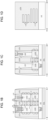
- FIGS. 1A-1F illustrate a 3D-stacked semiconductor device including contact structures having different contact areas on respective source/drain regions, according to one or more embodiments.
- FIG. 1A is a plan view of a 3D-stacked semiconductor device
- FIGS. 1B-1F are cross-section views of the 3D-stacked semiconductor device 10 shown in FIG. 1A taken along lines I-I', II-II', III-III, IV-IV', and V-V', respectively.
- FIG. 1A is provided to show a positional relationship between selected structural elements of the 3D-stacked semiconductor device 10, and thus, some structural elements such as a substrate and an isolation structure shown in FIGS. 1B-1F are not shown in FIG. 1A .
- a D1 direction is a channel-length direction in which a current flows between two source/drain regions connected to each other through a channel structure
- a D2 direction is a channel-width direction that intersects the D1 direction
- a D3 direction is a vertical direction that intersects the D1 and D2 directions both of which are horizontal directions.
- the 3D-stacked semiconductor device 10 may include a plurality of nanosheet layers forming a 1 st channel structure 110 at a 1 st level above a backside isolation structure 141, and a plurality of nanosheet layers forming a 2 nd channel structure 120 at a 2 nd level above the 1 st level.
- a middle isolation structure 115 may be formed between the 1 st channel structure 110 and the 2 nd channel structure 120.
- the nanosheet layers of the channel structures 110 and 120 may have been epitaxially grown from a silicon substrate which is replaced by the backside isolation structure 141 in manufacturing the 3D-stacked semiconductor device 10.
- the 1 st channel structure 110 may connect 1 st source/drain regions 135S and 135D to each other so that a current flows therebetween at a control of a gate structure 125B which surrounds the 1 st channel structure 110.
- the 2 nd channel structure 120 may connect 2 nd source/drain regions 145S and 145D to each other so that a current flows therebetween at a control of the gate structure 125B which surrounds the 2 nd channel structure 120.
- the gate structures 125A and 125C formed at both sides of the gate structure 125B are inactive gate structures in the 3D-stacked semiconductor device 10 herein.
- the 1 st source/drain regions 135S and 135D may be epitaxially grown from the 1 st channel structure 110 and the 2 nd source/drain regions 145S and 145D may be epitaxially grown from the 2 nd channel structure 120.
- the 1 st channel structure 110 along with the 1 st source/drain regions 135S, 135D and the gate structure 125B may form a 1 st transistor, which is a nanosheet transistor, at the 1 st level.
- the 2 nd channel structure 120 along with the 2 nd source/drain regions 145S, 145D and the gate structure 125B may form a 2 nd transistor, which is also a nanosheet transistor, at the 2 nd level.
- the 1 st source/drain regions 135S and 135D may function as a source and a drain, respectively, of the 1 st transistor
- 2 nd source/drain regions 145S and 145D may function as a source and a drain, respectively, of the 2 nd transistor.
- a frontside isolation structure 142 may be formed to surround each of the source/drain regions 135S, 135D, 145S and 145D to isolate these semiconductor structures from each other and other circuit elements.
- the gate structure 125B may be a common gate structure shared by the two transistors to form a complementary metal oxide semiconductor (CMOS) device structure such as an inverter circuit.
- CMOS complementary metal oxide semiconductor
- an additional isolation may be formed to separate the gate structure 125B into two gate structures for the 1 st transistor and the 2 nd transistor, respectively.
- Gate spacers 151 formed on side surfaces of the gate structures 125A-125B may have been used to protect dummy gate structures of polycrystalline silicon from various processes in manufacturing the 3D-stacked semiconductor device 10, and remain after the dummy gate structure is replaced by the gate structures 125A-125C to prevent current leakage therefrom to other circuit elements.
- Inner spacers 116 may be formed between the gate structures 125A-125B, surrounding the channel structures 110 and 120, and the source/drain regions 135S, 125D, 145S and 125D to prevent current leakage therebetween.
- the isolation structures 141 and 142 may each be formed of silicon oxide such as SiO 2 , not being limited thereto.
- Each semiconductor nanosheet layer forming the channel structures 110 and 120 may be formed of silicon (Si) or silicon germanium (SiGe).
- the 1 st source/drain regions 135S, 135D and the 2 nd source/drain regions 145S, 145D may also be formed of Si or SiGe.
- the 1 st source/drain regions 135S and 135D are formed of Si and doped with n-type impurities such as phosphorus (P), arsenic (As), antimony (Sb), etc.
- the 1 st transistor may be an n-type transistor.
- the 2 nd source/drain regions 145S and 145D are formed of SiGe and doped with impurities such as boron (B), gallium (Ga), indium (In), etc.
- the 2 nd transistor may be a p-type transistor.
- the gate structures 125A-125C may each include a gate dielectric layer and a conductor layer.
- the gate dielectric layer may include a high-k material such as Hf, Al, Zr, La, Mg, Ba, Ti, Pb, and/or a combination thereof, not being limited thereto
- the conductor layer may include a metal or metal compound such as Cu, Al, Ti, Ta, W, Co, TiN, WN, TiAl, TiAlN, TaN, TiC, TaC, TiAlC, TaCN, TaSiN, or a combination thereof, not being limited thereto.
- the inner spacers 116 may be formed of silicon nitride (e.g., SiN, SiBCN, SiCN, SiOCN, etc.), not being limited thereto.
- the gate spacers 151 may be formed of silicon oxide or silicon nitride (e.g., SiO2, SiN, SiBCN, SiCN, SiOC, SiOCN, etc.), not being limited thereto, which may be different from the material(s) forming the inner spacers 116.
- the 2 nd channel structure 120 may be formed to have a smaller width in the D2 direction than the 1 st channel structure 110.
- a left edge (or left side surface) of the 2 nd channel structure 120 is vertically aligned or coplanar with a left edge (or left side surface) of the 1 st channel structure 110
- a right edge (or right side surface) of the 2 nd channel structure 120 is not vertically aligned or coplanar with a right edge (or right side surface) of the 1 st channel structure 110.
- a right side of the 2 nd channel structure 120 and above the 1 st channel structure 110 may provide a non-overlapping region where the 2 nd channel structure 120 does not vertically overlap the 1 st channel structure 110.
- each of the 2 nd source/drain regions 145S and 145D epitaxially grown from the 2 nd channel structure 120 may also have a smaller width in the D2 direction than each of the 1 st source/drain regions 135S and 135D epitaxially grown from the 1 st channel structure 110, respectively.
- a right edge of the 2 nd source/drain region 145D is not vertically aligned or coplanar with a right edge of the 1 st source/drain region 135D.
- a right side of the 2 nd source/drain region 145D above the 1 st source/drain region 135D may provide a non-overlapping region where the 2 nd source/drain region 145D does not vertically overlap the 1 st source/drain region 135D.
- the foregoing width differences between the source/drain regions are provided to form a contact structure of the 1 st source/drain region 135D on at least a portion of the top surface of the 1 st source/drain region 135D through the non-overlapping region in a limited area, as shown in FIG. 1F .
- Each of the 1 st source/drain regions 135S and 135D and the 2 nd source/drain regions 145S and 145D may have a contact structure formed thereon for connection to a voltage source or another circuit element therethrough.
- the 1 st source/drain region 135S may have a backside contact structure BCA formed on a bottom surface thereof in the backside isolation structure 141.
- the backside contact structure BCA may connect the 1 st source/drain regions 135S to a negative voltage source VSS though a backside metal line BM1 formed in the backside isolation structure 141.
- the 1 st source/drain region 135D may have a 1 st contact structure CR formed on a right portion of a top surface.
- the 1 st contact structure CR may connect the 1 st source/drain region 135D to the 2 nd source/drain region 145D thereabove through a 2 nd contact structure CA2 formed on an upper-right portion of the 2 nd source/drain region 145D.
- the 2 nd source/drain region 145S may have a 2 nd contact structure CA1 formed on a left-upper portion of the 2 nd source/drain region 145S.
- the 2 nd contact structure CA1 may connect the 2 nd source/drain region 145S to a positive voltage source VDD through a 1 st front-side via RB, a 2 nd front-side via TB, and a backside metal line BM2.
- a gate contact structure (not shown) may be formed on the gate structure 125 to receive a gate input signal through a metal line included in a back-end-of-line (BEOL) layer.
- BEOL back-end-of-line
- a source/drain region being connected to a voltage source refers to the source/drain region being connected to the voltage source without through another source/drain region or a gate structure
- a source/drain region being connected to another circuit element refers to the source/drain region being connected to the other circuit element such as another source/drain region without through a voltage source.
- Each of the contact structures BCA, CR, CA1, CA2, the vias RB and TB, and the backside metal lines BM1 and BM2 may be formed of a metal or metal compound such as Cu, W, Al, Ru, Mo, Co, and/or a combination thereof, not being limited thereto.
- the 2 nd contact structure CA1 may be formed to have a large contact area on the 2 nd source/drain region 145S to decrease contact resistance therebetween while the 2 nd contact structure CA2 may be formed to have a small contact area on the 2 nd source/drain region 145D to reduce contact capacitance therebetween.
- the 2 nd contact structure CA1 may have a large contact length L1, a large contact width W1 and a large contact height H1 on the 2 nd source/drain region 145S, while the 2 nd contact structure CA1 may have a small contact length L2, a small contact width W2 and a small contact height H2 on the 2 nd source/drain region 145D, in the respective D1-D3 directions.
- the contact area difference may be implemented by differentiating only one or two of the contact length, the contact width and the contact height.
- a large contact area may be implemented by increasing only one or two of the contact length, the contact width and the contact height even if the other one or two are decreased.
- a small contact area may be implemented by decreasing one or two of the contact length, the contact width and the contact height even if the other one or two are increased.
- the foregoing contact area difference between the two 2 nd contact structures CA1 and CA2 is provided because the 2 nd contact structure CA1 is configured to receive and deliver power from the voltage source VDD to the 2 nd source/drain region 145S while the 2 nd contact structure CA2 is configured to transmit or receive a routing signal to or from another circuit element such as the 1 st source/drain region 135D of the 1 st transistor at the 1 st level.
- power delivery from the voltage source VDD to the 2 nd source/drain region 145S may be more effective and efficient when the 2 nd contact structure CA1 has a small contact resistance on the 2 nd source/drain region 145S.
- power consumption at the 2 nd source/drain region 145S may be reduced due to the small contact resistance caused by the large contact area.
- increase of capacitance between the 2 nd contact structure CA1 and the 2 nd source/drain region 145S because of the large contact area may not affect performance of the 3D-stacked semiconductor device 10 as much as the small contact resistance contributes to performance improvement in the 3D-stacked semiconductor device 10.
- the small contact capacitance caused by the small contact area between the 2 nd contact structure CA2 and the 2 nd source/drain region 145D may prevent increase of a switching time of an AC signal transmitted to or received from the 2 nd source/drain region 145D, thereby to reduce power consumption.
- increase of contact resistance between the 2 nd contact structure CA2 and the 2 nd source/drain region 145D because of the small contact area may not affect performance of the 3D-stacked semiconductor device 10 as much as the small contact capacitance contributes to improving performance of the 3D-stacked semiconductor device 10.
- a bottom surface of the 2 nd contact structure CA1 on the 2 nd source/drain region 145S may have a length L1 while a bottom surface of the 2 nd contact structure CA2 on the 2 nd source/drain region 145D may have a length L2 which is smaller than the length L1 in the D1 direction, as shown in FIG. 1B .
- a distance D2 between the 2 nd contact structure CA2 and the gate structure 125B may be greater than a distance D1 between the 2 nd contact structure CA1 and the gate structure 125B.
- fringe capacitance between the 2 nd contact structure CA2 and the gate structure 125B may be smaller than that between the 2 nd contact structure CA1 and the gate structure 125B.
- device performance may be additionally improved by decreasing an AC signal switching time, reducing power consumption, and reducing influence on a gate threshold voltage of the gate structure 125B.
- the 2 nd contact structures CA1 and CA2 may be formed by patterning the frontside isolation structure 142 on the 2 nd source/drain regions 145S and 145D between the gate structures 125A-125C. This patterning may expose top surfaces of the 2 nd source/drain regions 145S and 145D by the lengths L1 and L2 as shown in FIG. 1B through, for example, photolithography, masking, and etching such as dry and/or wet etching.
- a metal or metal compound such as Cu, W, Al, Ru, Mo, Co, and/or a combination thereof, may be deposited in the patterned frontside isolation structure 142 through, for example, physical vapor deposition (PVD), chemical vapor deposition (CVD), plasma enhanced chemical vapor deposition (PECVD), or a combination thereof, followed by planarization such as chemical-mechanical polishing (CMP), not being limited thereto.
- PVD physical vapor deposition
- CVD chemical vapor deposition
- PECVD plasma enhanced chemical vapor deposition
- CMP chemical-mechanical polishing
- the 2 nd contact structure CA1 and the 2 nd contact structure CA2 may be formed in a self-aligned manner according to one or more embodiments.
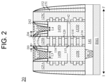
- FIG. 2 illustrates a 3D-stacked semiconductor device including contact structures having different contact areas on respective source/drain regions, according to one or more embodiments.
- a 3D-stacked semiconductor device 20 may include the same structural elements included in the 3D-stacked semiconductor device 10 of FIGS. 1A-1F except that 2 nd contact structures CA3 and CA4 may be formed in a frontside isolation structure 242 based on extra gate spacers 152 on side surfaces of the gate spacers 151.
- 2 nd contact structures CA3 and CA4 may be formed in a frontside isolation structure 242 based on extra gate spacers 152 on side surfaces of the gate spacers 151.
- the gate spacers 151 may be formed on the side surfaces of the gate structures 125A-125C and on the 2 nd source/drain regions 145S and 145D, and the frontside isolation structure 142 may be formed between the gate spacers 151 on the 2 nd source/drain regions 145S and 145D.
- the 2 nd contact structures CA1 and CA2 may be formed through the frontside isolation structure 142 to contact the top surfaces of the 2 nd source/drain regions 145S and 145D, respectively.
- side surfaces of the 2 nd contact structures CA1 and CA2 may be surrounded by the frontside isolation structure 142, and the contact lengths L1 and L2 of the 2 nd contact structures CA1 and CA2 on the 2 nd source/drain regions 145S and 145D may be defined, respectively, in the frontside isolation structure 142.
- the extra gate spacers 152 may be formed along the side surfaces of the gate spacers 151 on the gate structures 125B and 125C and on the 2 nd source/drain regions 145S and 145D.
- the extra gate spacers 152 may contact the side surfaces of these gate spacers 151, and bottom surfaces of the extra gate spacers 152 may contact top surfaces of the 2 nd source/drain regions 145S and 145D.
- the extra gate spacers 152 may be formed on the 2 nd source/drain regions 145S and 145D such that a contact length L3 of the 2 nd contact structure CA1 on the 2 nd source/drain region 145S is defined by a distance between the gate spacer 151 and the extra gate spacer 152 on the 2 nd source/drain region 145D, and a contact length L4 of the 2 nd contact structure CA2 on the 2 nd source/drain region 145D is defined by a distance between the extra gate spacers 152 on the 2 nd source/drain region 145D.
- the frontside isolation structure 242 may be formed between the gate spacer 151 and the extra gate spacer 152 on the 2 nd source/drain region 145S, and between the extra gate spacers 152 on the 2 nd source/drain region 145D. Further, the 2 nd contact structures CA3 and CA4 may be formed through the frontside isolation structure 242 to contact the top surfaces of the 2 nd source/drain regions 145S and 145D, respectively, as in the 3D-stacked semiconductor device 10 of FIGS. 1A-1F .
- the 2 nd contact structures CA3 and CA4 may formed through the frontside isolation structure 242
- lower edge portions of the 2 nd contact structure CA3 may contact the gate spacer 151 and the extra gate spacer 152 on the 2 nd source/drain region 145S without the frontside isolation structure 242 therebetween
- lower edge portions of the 2 nd contact structure CA4 may contact the extra gate spacers 152 on the 2 nd source/drain region 145D without the frontside isolation structure 242 therebetween.
- the contact lengths L3 and L4 of the 2 nd contact structures CA3 and CA4 on the 2 nd source/drain regions 145S and 145D may be defined, respectively, by the gate spacer 151 and the extra gate spacers 152.
- the frontside isolation structure 242 may have been patterned in a self-aligning manner due to the extra gate spacers 152 as well as the gate spacer 151 to provide respective contact holes to expose respective contact areas including the contact lengths L3 and L4 on the 2 nd source/drain regions 145S and 145D.
- a combination of chlorotrifluoride (CHF 3 ) and hydrogen (H 2 ) may be used an etchant for reactive ion etching (RIE) to selectively etch the frontside isolation structure 242 formed of silicon oxide such as SiO 2 against silicon nitride such as SiBCN.
- RIE reactive ion etching
- the frontside isolation structure 242 may be removed at around lower edges of the gate spacer 151 and the extra gate spacers 152 on the 2 nd source/drain regions 145S and 145D, so that the lower edge portions of the 2 nd contact structures CA3 and CA4 may contact the gate spacer 151 and the extra gate spacers 152 on the 2 nd source/drain regions 145S and 145D as described above without the frontside isolation structure 242 therebetween.
- the 3D-stacked semiconductor device 20 may still be characterized by a difference in contact areas of the 2 nd contact structures CA3 and CA4 on the 2 nd source/drain regions 145D and 145S, respectively.
- the 2 nd contact structure CA3 on the 2 nd source/drain region 145S may be have a greater area than the 2 nd contact structure CA4 on the 2 nd source/drain region 145D considering that the 2 nd contact structure CA3 connects the 2 nd source/drain region 145S to the voltage source VDD and the 2 nd contact structure CA4 connects the 2 nd source/drain region 145D to another circuit element such as the 1 st source/drain region 135D of the 1 st transistor at the 1 st level.
- the contact length L3 of a bottom surface of the 2 nd contact structure CA1 defined by the gate spacer 151 and the extra gate spacer 152 on the 2 nd source/drain region 145S may be greater than the contact length L4 of a bottom surface of the 2 nd contact structure CA2 defined by the extra gate spacers 152 on the 2 nd source/drain regions 145D by a length of the extra gate spacer 152 in the D1 direction.
- the contact area difference in the 3D-stacked semiconductor device 20 may be implemented considering that contact resistance is the priority factor for power delivery performance by the 2 nd contact structure CA3 to the 2 nd source/drain region 145S, and contact capacitance is the priority factor for signal routing performance by the 2 nd contact structure CA4 with respect to the 2 nd source/drain region 145D.
- the 2 nd contact structure CA3 configured to deliver power from the voltage source VDD to the 2 nd source/drain region 145S is less sensitive to contact capacitance, while the 2 nd contact structure CA4 configured to receive or transmit a signal from or to the 2 nd source/drain region 145D for signal routing purposes rather than power delivery to the 2 nd source/drain region 145D is less sensitive to contact resistance.
- a distance D4 between the 2 nd contact structure CA4 and the gate structure 125B may be greater than a distance D3 between the 2 nd contact structure CA3 and the gate structure 125B.
- fringe capacitance between the 2 nd contact structure CA4 and the gate structure 125B may be smaller than that between the 2 nd contact structure CA3 and the gate structure 125B.
- device performance may be additionally improved by decreasing an AC signal switching time, reducing power consumption, and reducing influence on a gate threshold voltage of the gate structure 125B.
- the 3D-stacked semiconductor devices 10 and 20 are described as being formed by nanosheet transistors. However, the disclosure is not limited thereto, and at least one of the 1 st and 2 nd transistors at the 1 st and 2 nd levels, respectively, in each of the 3D-stacked semiconductor devices 10 and 20 may be formed by a different type of transistor such as FinFET and forksheet transistor, according to one or more embodiments.
- the 1 st and 2 nd transistors are described as p-type and n-type transistors. However, the disclosure is not limited thereto, and each of the 1 st and 2 nd transistors may be of either p-type or n-type, according to one or more embodiments.
- FIG. 3 illustrates a flowchart of a method of manufacturing a semiconductor device including contact structures having different contact areas on respective source/drain regions, according to one or more embodiments.
- the semiconductor device manufactured according to the flowchart of FIG. 3 may correspond to the 3D-stacked semiconductor device 10 or 20 shown in FIGS. 1A-1F and 2 , and thus, materials and functions of structural elements of the semiconductor device may be the same as those of the 3D-stacked semiconductor device 10 or 20 described above, and thus, duplicate descriptions thereof are omitted herein.
- a transistor structure may be provided, including a channel structure, three gate structures with gate spacers thereon, a 1 st source/drain region, and a 2 nd source/drain region to be connected to a voltage source and another circuit element, respectively.
- the 1 st and 2 nd source/drain regions may be formed by epitaxial growth from the channel structure, and the gate structures may be formed by replacing dummy gate structures on the channel structure.
- the gate spacers may be formed on respective side surfaces of the dummy gate structures to protect the dummy gate structures from various operations including formation of the 1 st and 2 nd source/drain regions, and remain after the dummy gate structures are replaced by the gate structures at least to prevent current leakage from the gate structures when the semiconductor device is completed and active.
- the channel structure may be formed of a plurality of nanosheet semiconductor layers to form the transistor structure as a nanosheet transistor or a forksheet transistor, or may be formed of one or more fin structures to form the transistor structure as a FinFET.
- the 1 st source/drain region may be configured to receive a power from a voltage source, and the 2 nd source/drain region may be configured to receive or transmit an AC signal from or to another circuit element in the semiconductor device or outside the semiconductor device.
- an isolation structure may be formed to surround the transistor structure provided in the previous step such that the isolation structure is formed on the 1 st and 2 nd source/drain regions.
- the isolation structure may be formed to isolate the 1 st and 2 nd source/drain regions from each other and other circuit elements.
- the formation of the isolation structure may be performed through, for example, PVD, CVD, PECVD, or a combination thereof, followed by planarization such as chemical-mechanical polishing (CMP), not being limited thereto.
- CMP chemical-mechanical polishing
- the isolation structure may be patterned to provide 1 st and 2 nd contact holes exposing portions of the 1 st and 2 nd source/drain regions such that the 1 st contact hole exposes a greater contact area on the 1 st source/drain region than the 2 nd contact hole on the 2 nd source/drain region.
- the isolation structure may be patterned based on hard mask structures formed thereon such that the 1 st contact hole exposes the 1 st source/drain region by a 1 st contact area and the 2 nd contact hole exposes the 2 nd source/drain region by a 2 nd contact area.
- the 1 st and 2 nd contact holes may be through holes, and the 1 st contact area is greater than the 2 nd contact area.
- the 1 st contact area can be greater than the 2 nd contact area by controlling at least one of a contact length, a contact width and a contact height formed by each of the 1 st and the 2 nd contact holes.
- the patterning operation in this step may be performed through, for example, dry etching and/or wet etching.
- the 1 st and 2 nd contact structures may be formed through the 1 st and 2 nd contact holes in the isolation structure, respectively, so that the 1 st contact structure on the 1 st source/drain region can have a greater contact area than the 2 nd contact structure on the 2 nd source/drain region.
- the 1 st contact structure connecting the 1 st source/drain region to a voltage source may have a smaller contact resistance and a greater contact capacitance with respect to the 1 st source/drain region
- the 2 nd contact structure connecting the 2 nd source/drain region to another circuit element such as another source/drain region or gate structure may have a smaller contact capacitance and a greater contact resistance with respect to the 2 nd source/drain region.
- the semiconductor device manufactured through the above steps may have an improved device performance in power delivery and signal routing.
- extra gate spacers may be formed on side surfaces of selected two gate structures among the three gate structures as optional step S15.
- the isolation structure can be patterned in a self-aligning manner to form a 2 nd contact hole based on the extra gate spacers thereon and form a 1 st contact hole based on the extra gate spacer and the gate spacer on the non-selected gate structure.
- the 2 nd contact hole may expose a smaller 2 nd contact area on the 2 nd source/drain region than a 1 st contact area exposed by the 1 st contact hole on the 1 st source/drain region.
- the extra gate spacers may facilitate the formation of the 1 st and 2 nd contact structures having different contact areas on the 1 st and 2 nd source/drain regions, respectively.
- FIG. 4 is a schematic block diagram illustrating an electronic device including a semiconductor device in which contact structures having different contact areas are formed on respective source/drain regions, according to one or more embodiments.
- This semiconductor device may be one of the 3D-stacked semiconductor devices 10 and 20 shown in FIGS. 1A-1F and 2 or a semiconductor device manufactured according to the method described in reference to FIG. 3 .
- an electronic device 1000 may include at least one processor 1100, a communication module 1200, an input/output module 1300, a storage 1400, and a buffer random access memory (RAM) module 1500.
- the electronic device 1000 may be a mobile device such as a smartphone or a tablet computer, not being limited thereto, according to embodiments.
- the processor 1100 may include a central processing unit (CPU), a graphic processing unit (GPU) and/or any other processors that control operations of the electronic device 1000.
- the communication module 1200 may be implemented to perform wireless or wire communications with an external device.
- the input/output module 1300 may include at least one of a touch sensor, a touch panel a key board, a mouse, a proximate sensor, a microphone, etc. to receive an input, and at least one of a display, a speaker, etc. to generate an output signal processed by the processor 1100.
- the storage 1400 may be implemented to store user data input through the input/output module 1300, the output signal, etc.
- the storage 1400 may be an embedded multimedia card (eMMC), a solid state drive (SSD), a universal flash storage (UFS) device, etc.
- eMMC embedded multimedia card
- SSD solid state drive
- UFS universal flash storage
- the buffer RAM module 1500 may temporarily store data used for processing operations of the electronic device 1000.
- the buffer RAM 1500 may include a volatile memory such as double data rate (DDR) synchronous dynamic random access memory (SDRAM), low power double data rate (LPDDR) SDRAM, graphics double data rate (GDDR) SDRAM, Rambus dynamic random access memory (RDRAM), etc.
- DDR double data rate
- SDRAM synchronous dynamic random access memory
- LPDDR low power double data rate SDRAM
- graphics double data rate SDRAM graphics double data rate SDRAM
- RDRAM Rambus dynamic random access memory
- the electronic device 1000 may further include at least one sensor such as an image sensor.
- At least one component in the electronic device 1000 may be formed based on a semiconductor device including contact structures having different contact areas on respective source/drain regions, according to one or more embodiments.
Landscapes
- Physics & Mathematics (AREA)
- Engineering & Computer Science (AREA)
- Condensed Matter Physics & Semiconductors (AREA)
- General Physics & Mathematics (AREA)
- Computer Hardware Design (AREA)
- Microelectronics & Electronic Packaging (AREA)
- Power Engineering (AREA)
- Insulated Gate Type Field-Effect Transistor (AREA)
- Metal-Oxide And Bipolar Metal-Oxide Semiconductor Integrated Circuits (AREA)
- Geometry (AREA)
- Thin Film Transistor (AREA)
- Manufacturing & Machinery (AREA)
Applications Claiming Priority (2)
| Application Number | Priority Date | Filing Date | Title |
|---|---|---|---|
| US202363548325P | 2023-11-13 | 2023-11-13 | |
| US18/606,001 US20250159979A1 (en) | 2023-11-13 | 2024-03-15 | Semiconductor device including contact structures having different dimensions |
Publications (2)
| Publication Number | Publication Date |
|---|---|
| EP4565027A2 true EP4565027A2 (de) | 2025-06-04 |
| EP4565027A3 EP4565027A3 (de) | 2025-08-27 |
Family
ID=93463268
Family Applications (1)
| Application Number | Title | Priority Date | Filing Date |
|---|---|---|---|
| EP24212137.4A Pending EP4565027A3 (de) | 2023-11-13 | 2024-11-11 | Halbleiterbauelement mit kontaktstrukturen mit unterschiedlichen abmessungen |
Country Status (5)
| Country | Link |
|---|---|
| US (1) | US20250159979A1 (de) |
| EP (1) | EP4565027A3 (de) |
| KR (1) | KR20250070558A (de) |
| CN (1) | CN119997599A (de) |
| TW (1) | TW202531884A (de) |
Family Cites Families (5)
| Publication number | Priority date | Publication date | Assignee | Title |
|---|---|---|---|---|
| US8679968B2 (en) * | 2012-05-15 | 2014-03-25 | Globalfoundries Singapore Pte. Ltd | Method for forming a self-aligned contact opening by a lateral etch |
| US20230180451A1 (en) * | 2021-12-03 | 2023-06-08 | Taiwan Semiconductor Manufacturing Company, Ltd. | Semiconductor Structure With Source/Drain Contact Plugs And Method For Forming The Same |
| KR20230134687A (ko) * | 2022-03-15 | 2023-09-22 | 삼성전자주식회사 | 반도체 소자 및 그의 제조 방법 |
| US12417941B2 (en) * | 2022-03-22 | 2025-09-16 | Taiwan Semiconductor Manufacturing Company, Ltd. | Isolation structures in semiconductor devices |
| US12356682B2 (en) * | 2022-05-20 | 2025-07-08 | Taiwan Semiconductor Manufacturing Company, Ltd. | Semiconductor structure with conductive structure |
-
2024
- 2024-03-15 US US18/606,001 patent/US20250159979A1/en active Pending
- 2024-09-24 KR KR1020240129420A patent/KR20250070558A/ko active Pending
- 2024-11-11 CN CN202411601553.2A patent/CN119997599A/zh active Pending
- 2024-11-11 EP EP24212137.4A patent/EP4565027A3/de active Pending
- 2024-11-12 TW TW113143393A patent/TW202531884A/zh unknown
Also Published As
| Publication number | Publication date |
|---|---|
| TW202531884A (zh) | 2025-08-01 |
| EP4565027A3 (de) | 2025-08-27 |
| CN119997599A (zh) | 2025-05-13 |
| KR20250070558A (ko) | 2025-05-20 |
| US20250159979A1 (en) | 2025-05-15 |
Similar Documents
| Publication | Publication Date | Title |
|---|---|---|
| US10403717B2 (en) | Semiconductor devices including contact structures that partially overlap silicide layers | |
| US10930652B2 (en) | Apparatuses including buried digit lines | |
| CN102446919B (zh) | 具有垂直沟道晶体管的半导体存储器件及其制造方法 | |
| EP4421859A1 (de) | Halbleiterbauelement mit auf basis einer kontaktisolationsschicht geformter selbstausgerichteter rückseitenkontaktstruktur | |
| EP4495986A1 (de) | 3d-gestapelte halbleitervorrichtung und verfahren zur herstellung davon | |
| EP4565027A2 (de) | Halbleiterbauelement mit kontaktstrukturen mit unterschiedlichen abmessungen | |
| US20240282855A1 (en) | Semiconductor device including 3d-stacked field-effect transistors having isolation structure between contact plugs | |
| US20240379780A1 (en) | 3d-stacked semiconductor device including source/drain regions vertically isolated from each other by strengthened isolation structure | |
| US11355640B1 (en) | Hybrid multi-stack semiconductor device including self-aligned channel structure and method of manufacturing the same | |
| US12211837B1 (en) | Semiconductor device including gate contact structure formed from gate structure | |
| US20250120183A1 (en) | Semiconductor device including gate contact structure formed from gate structure | |
| EP4608091A2 (de) | Halbleiterbauelement mit gabelschichttransistoren mit isolationswand und gate-schnitt-struktur darauf | |
| US20250254988A1 (en) | Semiconductor device including stacked forksheet transistor structure with isolation wall | |
| US20250142871A1 (en) | Semiconductor device including dual contact structures on source/drain region | |
| US20250040242A1 (en) | 3d-stacked semiconductor device including middle isolation structure and bspdn structure | |
| EP4535957A1 (de) | Halbleiterbauelement mit gate-kontaktstruktur aus der gate-struktur | |
| US20250159986A1 (en) | Cut-mask patterning to remove corner- rounding of active regions of semiconductor device | |
| US20250081562A1 (en) | Semiconductor device including source/drain region with underblocking layer thereon | |
| EP4333061A1 (de) | Feldeffekttransistorstruktur mit passivem beuelement oder bipolartransistor mit rückseitigem stromverteilungsnetzwerk (bspdn) | |
| US20250098324A1 (en) | 3d-stacked semiconductor device having different channel structures, source/drain regions, and gate structures at different levels | |
| US20240290853A1 (en) | Semiconductor device including extended backside contact structure | |
| CN118553768A (zh) | 包括扩展背侧接触结构的半导体器件及其制造方法 |
Legal Events
| Date | Code | Title | Description |
|---|---|---|---|
| PUAI | Public reference made under article 153(3) epc to a published international application that has entered the european phase |
Free format text: ORIGINAL CODE: 0009012 |
|
| STAA | Information on the status of an ep patent application or granted ep patent |
Free format text: STATUS: THE APPLICATION HAS BEEN PUBLISHED |
|
| AK | Designated contracting states |
Kind code of ref document: A2 Designated state(s): AL AT BE BG CH CY CZ DE DK EE ES FI FR GB GR HR HU IE IS IT LI LT LU LV MC ME MK MT NL NO PL PT RO RS SE SI SK SM TR |
|
| PUAL | Search report despatched |
Free format text: ORIGINAL CODE: 0009013 |
|
| AK | Designated contracting states |
Kind code of ref document: A3 Designated state(s): AL AT BE BG CH CY CZ DE DK EE ES FI FR GB GR HR HU IE IS IT LI LT LU LV MC ME MK MT NL NO PL PT RO RS SE SI SK SM TR |
|
| RIC1 | Information provided on ipc code assigned before grant |
Ipc: H10D 30/01 20250101AFI20250722BHEP Ipc: H10D 30/00 20250101ALI20250722BHEP Ipc: H10D 84/01 20250101ALI20250722BHEP Ipc: H10D 84/83 20250101ALI20250722BHEP Ipc: H10D 64/23 20250101ALI20250722BHEP Ipc: H10D 64/01 20250101ALI20250722BHEP Ipc: H10D 64/66 20250101ALI20250722BHEP |