EP4560703A2 - Power overlay package for a semiconductor device - Google Patents
Power overlay package for a semiconductor device Download PDFInfo
- Publication number
- EP4560703A2 EP4560703A2 EP25161713.0A EP25161713A EP4560703A2 EP 4560703 A2 EP4560703 A2 EP 4560703A2 EP 25161713 A EP25161713 A EP 25161713A EP 4560703 A2 EP4560703 A2 EP 4560703A2
- Authority
- EP
- European Patent Office
- Prior art keywords
- pad
- pol
- package
- rdl
- semiconductor device
- Prior art date
- Legal status (The legal status is an assumption and is not a legal conclusion. Google has not performed a legal analysis and makes no representation as to the accuracy of the status listed.)
- Pending
Links
Images


Classifications
-
- H—ELECTRICITY
- H10—SEMICONDUCTOR DEVICES; ELECTRIC SOLID-STATE DEVICES NOT OTHERWISE PROVIDED FOR
- H10W—GENERIC PACKAGES, INTERCONNECTIONS, CONNECTORS OR OTHER CONSTRUCTIONAL DETAILS OF DEVICES COVERED BY CLASS H10
- H10W90/00—Package configurations
- H10W90/701—Package configurations characterised by the relative positions of pads or connectors relative to package parts
-
- H—ELECTRICITY
- H10—SEMICONDUCTOR DEVICES; ELECTRIC SOLID-STATE DEVICES NOT OTHERWISE PROVIDED FOR
- H10W—GENERIC PACKAGES, INTERCONNECTIONS, CONNECTORS OR OTHER CONSTRUCTIONAL DETAILS OF DEVICES COVERED BY CLASS H10
- H10W72/00—Interconnections or connectors in packages
- H10W72/90—Bond pads, in general
-
- H—ELECTRICITY
- H10—SEMICONDUCTOR DEVICES; ELECTRIC SOLID-STATE DEVICES NOT OTHERWISE PROVIDED FOR
- H10W—GENERIC PACKAGES, INTERCONNECTIONS, CONNECTORS OR OTHER CONSTRUCTIONAL DETAILS OF DEVICES COVERED BY CLASS H10
- H10W70/00—Package substrates; Interposers; Redistribution layers [RDL]
- H10W70/60—Insulating or insulated package substrates; Interposers; Redistribution layers
- H10W70/62—Insulating or insulated package substrates; Interposers; Redistribution layers characterised by their interconnections
- H10W70/65—Shapes or dispositions of interconnections
- H10W70/658—Shapes or dispositions of interconnections for devices provided for in groups H10D8/00 - H10D48/00
-
- H—ELECTRICITY
- H10—SEMICONDUCTOR DEVICES; ELECTRIC SOLID-STATE DEVICES NOT OTHERWISE PROVIDED FOR
- H10W—GENERIC PACKAGES, INTERCONNECTIONS, CONNECTORS OR OTHER CONSTRUCTIONAL DETAILS OF DEVICES COVERED BY CLASS H10
- H10W70/00—Package substrates; Interposers; Redistribution layers [RDL]
- H10W70/01—Manufacture or treatment
- H10W70/05—Manufacture or treatment of insulating or insulated package substrates, or of interposers, or of redistribution layers
-
- H—ELECTRICITY
- H10—SEMICONDUCTOR DEVICES; ELECTRIC SOLID-STATE DEVICES NOT OTHERWISE PROVIDED FOR
- H10W—GENERIC PACKAGES, INTERCONNECTIONS, CONNECTORS OR OTHER CONSTRUCTIONAL DETAILS OF DEVICES COVERED BY CLASS H10
- H10W70/00—Package substrates; Interposers; Redistribution layers [RDL]
- H10W70/01—Manufacture or treatment
- H10W70/05—Manufacture or treatment of insulating or insulated package substrates, or of interposers, or of redistribution layers
- H10W70/095—Manufacture or treatment of insulating or insulated package substrates, or of interposers, or of redistribution layers of vias therein
-
- H—ELECTRICITY
- H10—SEMICONDUCTOR DEVICES; ELECTRIC SOLID-STATE DEVICES NOT OTHERWISE PROVIDED FOR
- H10W—GENERIC PACKAGES, INTERCONNECTIONS, CONNECTORS OR OTHER CONSTRUCTIONAL DETAILS OF DEVICES COVERED BY CLASS H10
- H10W70/00—Package substrates; Interposers; Redistribution layers [RDL]
- H10W70/40—Leadframes
- H10W70/479—Leadframes on or in insulating or insulated package substrates, interposers, or redistribution layers
-
- H—ELECTRICITY
- H10—SEMICONDUCTOR DEVICES; ELECTRIC SOLID-STATE DEVICES NOT OTHERWISE PROVIDED FOR
- H10W—GENERIC PACKAGES, INTERCONNECTIONS, CONNECTORS OR OTHER CONSTRUCTIONAL DETAILS OF DEVICES COVERED BY CLASS H10
- H10W70/00—Package substrates; Interposers; Redistribution layers [RDL]
- H10W70/60—Insulating or insulated package substrates; Interposers; Redistribution layers
-
- H—ELECTRICITY
- H10—SEMICONDUCTOR DEVICES; ELECTRIC SOLID-STATE DEVICES NOT OTHERWISE PROVIDED FOR
- H10W—GENERIC PACKAGES, INTERCONNECTIONS, CONNECTORS OR OTHER CONSTRUCTIONAL DETAILS OF DEVICES COVERED BY CLASS H10
- H10W70/00—Package substrates; Interposers; Redistribution layers [RDL]
- H10W70/60—Insulating or insulated package substrates; Interposers; Redistribution layers
- H10W70/611—Insulating or insulated package substrates; Interposers; Redistribution layers for connecting multiple chips together
-
- H—ELECTRICITY
- H10—SEMICONDUCTOR DEVICES; ELECTRIC SOLID-STATE DEVICES NOT OTHERWISE PROVIDED FOR
- H10W—GENERIC PACKAGES, INTERCONNECTIONS, CONNECTORS OR OTHER CONSTRUCTIONAL DETAILS OF DEVICES COVERED BY CLASS H10
- H10W70/00—Package substrates; Interposers; Redistribution layers [RDL]
- H10W70/60—Insulating or insulated package substrates; Interposers; Redistribution layers
- H10W70/62—Insulating or insulated package substrates; Interposers; Redistribution layers characterised by their interconnections
- H10W70/63—Vias, e.g. via plugs
- H10W70/635—Through-vias
-
- H—ELECTRICITY
- H10—SEMICONDUCTOR DEVICES; ELECTRIC SOLID-STATE DEVICES NOT OTHERWISE PROVIDED FOR
- H10W—GENERIC PACKAGES, INTERCONNECTIONS, CONNECTORS OR OTHER CONSTRUCTIONAL DETAILS OF DEVICES COVERED BY CLASS H10
- H10W70/00—Package substrates; Interposers; Redistribution layers [RDL]
- H10W70/60—Insulating or insulated package substrates; Interposers; Redistribution layers
- H10W70/62—Insulating or insulated package substrates; Interposers; Redistribution layers characterised by their interconnections
- H10W70/65—Shapes or dispositions of interconnections
-
- H—ELECTRICITY
- H10—SEMICONDUCTOR DEVICES; ELECTRIC SOLID-STATE DEVICES NOT OTHERWISE PROVIDED FOR
- H10W—GENERIC PACKAGES, INTERCONNECTIONS, CONNECTORS OR OTHER CONSTRUCTIONAL DETAILS OF DEVICES COVERED BY CLASS H10
- H10W70/00—Package substrates; Interposers; Redistribution layers [RDL]
- H10W70/60—Insulating or insulated package substrates; Interposers; Redistribution layers
- H10W70/62—Insulating or insulated package substrates; Interposers; Redistribution layers characterised by their interconnections
- H10W70/65—Shapes or dispositions of interconnections
- H10W70/652—Cross-sectional shapes
-
- H—ELECTRICITY
- H10—SEMICONDUCTOR DEVICES; ELECTRIC SOLID-STATE DEVICES NOT OTHERWISE PROVIDED FOR
- H10W—GENERIC PACKAGES, INTERCONNECTIONS, CONNECTORS OR OTHER CONSTRUCTIONAL DETAILS OF DEVICES COVERED BY CLASS H10
- H10W70/00—Package substrates; Interposers; Redistribution layers [RDL]
- H10W70/60—Insulating or insulated package substrates; Interposers; Redistribution layers
- H10W70/62—Insulating or insulated package substrates; Interposers; Redistribution layers characterised by their interconnections
- H10W70/66—Conductive materials thereof
-
- H—ELECTRICITY
- H10—SEMICONDUCTOR DEVICES; ELECTRIC SOLID-STATE DEVICES NOT OTHERWISE PROVIDED FOR
- H10W—GENERIC PACKAGES, INTERCONNECTIONS, CONNECTORS OR OTHER CONSTRUCTIONAL DETAILS OF DEVICES COVERED BY CLASS H10
- H10W70/00—Package substrates; Interposers; Redistribution layers [RDL]
- H10W70/60—Insulating or insulated package substrates; Interposers; Redistribution layers
- H10W70/67—Insulating or insulated package substrates; Interposers; Redistribution layers characterised by their insulating layers or insulating parts
- H10W70/68—Shapes or dispositions thereof
-
- H—ELECTRICITY
- H10—SEMICONDUCTOR DEVICES; ELECTRIC SOLID-STATE DEVICES NOT OTHERWISE PROVIDED FOR
- H10W—GENERIC PACKAGES, INTERCONNECTIONS, CONNECTORS OR OTHER CONSTRUCTIONAL DETAILS OF DEVICES COVERED BY CLASS H10
- H10W72/00—Interconnections or connectors in packages
- H10W72/01—Manufacture or treatment
- H10W72/019—Manufacture or treatment of bond pads
-
- H—ELECTRICITY
- H10—SEMICONDUCTOR DEVICES; ELECTRIC SOLID-STATE DEVICES NOT OTHERWISE PROVIDED FOR
- H10W—GENERIC PACKAGES, INTERCONNECTIONS, CONNECTORS OR OTHER CONSTRUCTIONAL DETAILS OF DEVICES COVERED BY CLASS H10
- H10W72/00—Interconnections or connectors in packages
- H10W72/071—Connecting or disconnecting
- H10W72/073—Connecting or disconnecting of die-attach connectors
- H10W72/07351—Connecting or disconnecting of die-attach connectors characterised by changes in properties of the die-attach connectors during connecting
- H10W72/07352—Connecting or disconnecting of die-attach connectors characterised by changes in properties of the die-attach connectors during connecting changes in structures or sizes
-
- H—ELECTRICITY
- H10—SEMICONDUCTOR DEVICES; ELECTRIC SOLID-STATE DEVICES NOT OTHERWISE PROVIDED FOR
- H10W—GENERIC PACKAGES, INTERCONNECTIONS, CONNECTORS OR OTHER CONSTRUCTIONAL DETAILS OF DEVICES COVERED BY CLASS H10
- H10W72/00—Interconnections or connectors in packages
- H10W72/30—Die-attach connectors
-
- H—ELECTRICITY
- H10—SEMICONDUCTOR DEVICES; ELECTRIC SOLID-STATE DEVICES NOT OTHERWISE PROVIDED FOR
- H10W—GENERIC PACKAGES, INTERCONNECTIONS, CONNECTORS OR OTHER CONSTRUCTIONAL DETAILS OF DEVICES COVERED BY CLASS H10
- H10W80/00—Direct bonding of chips, wafers or substrates
- H10W80/701—Direct bonding of chips, wafers or substrates characterised by the pads after the direct bonding
- H10W80/732—Direct bonding of chips, wafers or substrates characterised by the pads after the direct bonding having shape changed during the connecting
-
- H—ELECTRICITY
- H10—SEMICONDUCTOR DEVICES; ELECTRIC SOLID-STATE DEVICES NOT OTHERWISE PROVIDED FOR
- H10W—GENERIC PACKAGES, INTERCONNECTIONS, CONNECTORS OR OTHER CONSTRUCTIONAL DETAILS OF DEVICES COVERED BY CLASS H10
- H10W72/00—Interconnections or connectors in packages
- H10W72/071—Connecting or disconnecting
- H10W72/073—Connecting or disconnecting of die-attach connectors
- H10W72/07331—Connecting techniques
- H10W72/07337—Connecting techniques using a polymer adhesive, e.g. an adhesive based on silicone or epoxy
-
- H—ELECTRICITY
- H10—SEMICONDUCTOR DEVICES; ELECTRIC SOLID-STATE DEVICES NOT OTHERWISE PROVIDED FOR
- H10W—GENERIC PACKAGES, INTERCONNECTIONS, CONNECTORS OR OTHER CONSTRUCTIONAL DETAILS OF DEVICES COVERED BY CLASS H10
- H10W72/00—Interconnections or connectors in packages
- H10W72/20—Bump connectors, e.g. solder bumps or copper pillars; Dummy bumps; Thermal bumps
- H10W72/231—Shapes
- H10W72/234—Cross-sectional shape, i.e. in side view
-
- H—ELECTRICITY
- H10—SEMICONDUCTOR DEVICES; ELECTRIC SOLID-STATE DEVICES NOT OTHERWISE PROVIDED FOR
- H10W—GENERIC PACKAGES, INTERCONNECTIONS, CONNECTORS OR OTHER CONSTRUCTIONAL DETAILS OF DEVICES COVERED BY CLASS H10
- H10W72/00—Interconnections or connectors in packages
- H10W72/20—Bump connectors, e.g. solder bumps or copper pillars; Dummy bumps; Thermal bumps
- H10W72/241—Dispositions, e.g. layouts
- H10W72/244—Dispositions, e.g. layouts relative to underlying supporting features, e.g. bond pads, RDLs or vias
Definitions
- the present disclosure relates generally to semiconductor devices, and more particularly to semiconductor devices having a power overlay package.
- Power semiconductor assemblies include devices used as switches or rectifiers in power electronic circuits, such as switched mode power supplies and the like. Power semiconductor devices are used in high voltage power applications to carry large amounts of current and to support large voltages. In use, high voltage power semiconductor devices are connected to an external circuit by way of power overlay ("POL") packages and an interconnect system.
- POL power overlay
- a POL package is layered onto a semiconductor device.
- the semiconductor device includes at least one source pad and a gate pad disposed on a top surface of the semiconductor device.
- the POL package includes at least one POL interconnect layer configured as a routing layer.
- the at least one POL interconnect layer is laminated with at least one dielectric layer (also referred to as an isolation film) deposited on the semiconductor device, and metallization vias extending through the dielectric layer.
- the metallization vias electrically couple the at least one source pad of the semiconductor device to a source pad disposed on a top surface of the dielectric layer, while a gate pad disposed on the top surface of the dielectric layer is coupled to the gate pad of the semiconductor device.
- a contact pad (such as a Kelvin contact) disposed on the top surface of the dielectric layer is electrically coupled to the source pad of the dielectric layer.
- POL packages generally utilize connections to electrically couple to the source pad, to the contact pad, and to the gate pad on the dielectric layer to deliver power to the semiconductor device through the metallization vias.
- the source pad, the contact pad, and the gate pad on the dielectric layer require sufficient surface area to solder, sinter, copper bond, copper clip, or otherwise connect the source pad, the contact pad, and the gate pad with the connections.
- the surface areas of the source pad, the contact pad, and the gate pad are generally limited by the overall surface area of the semiconductor device.
- direct soldering, sintering, copper bonding, and copper clipping to the source pad and the gate pad on the semiconductor device, without a POL package introduces bonding stresses onto the semiconductor device.
- the introduction of the source pad, the contact pad, and the gate pad on the dielectric layer of the POL package provides stress buffering and reduces the stress on to the semiconductor device.
- a semiconductor assembly including a semiconductor device and a POL-RDL package coupled to said semiconductor device.
- the device includes an upper surface, a gate pad disposed on said upper surface; and at least one source pad disposed on said upper surface.
- the POL-RDL package includes a dielectric layer comprising an upper surface, at least one source pad disposed on said upper surface of said dielectric layer and electrically coupled to said at least one source pad of said semiconductor device; at least one contact pad disposed on said upper surface of said dielectric layer; and at least one trace connection having a resistivity value and electrically coupling said at least one source pad of said POL-RDL package to said at least one contact pad.
- method of manufacturing a semiconductor assembly includes coupling a dielectric layer of a POL-RDL package to an upper surface of a semiconductor device, the semiconductor device including at least one source pad and a gate pad disposed on the upper surface; forming at least one source pad of the POL-RDL package on an upper surface of the dielectric layer; electrically coupling the at least one source pad of the POL-RDL package to the at least one source pad of the semiconductor device; forming a gate pad of the POL-RDL package on the upper surface of the dielectric layer; electrically coupling the gate pad of the POL-RDL package to the gate pad of the semiconductor device; forming at least one contact pad on the upper surface of the dielectric layer; and electrically coupling the at least one source pad of the POL-RDL package to the at least one contact pad using at least one trace connection having a resistivity value.
- approximating language such as “generally,” “substantially,” and “about,” as used herein indicates that the term so modified may apply to only an approximate degree, as would be recognized by one of ordinary skill in the art, rather than to an absolute or perfect degree. Accordingly, a value modified by a term or terms, such as “about,” “approximately,” and “substantially,” is not to be limited to the precise value specified. In at least some instances, the approximating language may correspond to the precision of an instrument for measuring the value.
- range limitations may be identified. Such ranges may be combined and/or interchanged, and include all the sub-ranges contained therein unless context or language indicates otherwise.
- first ⁇ ⁇ ⁇ ⁇ ⁇ ⁇ ⁇ ⁇ ⁇ ⁇ ⁇ ⁇ ⁇ ⁇ ⁇ ⁇ ⁇ ⁇ ⁇ ⁇ ⁇ ⁇ ⁇ ⁇ ⁇ ⁇ ⁇ ⁇ ⁇ ⁇ ⁇ ⁇ ⁇ ⁇ ⁇ ⁇ ⁇ ⁇ ⁇ ⁇ ⁇ ⁇ ⁇ ⁇ ⁇ ⁇ ⁇ ⁇ ⁇ ⁇ ⁇ ⁇ ⁇ ⁇ ⁇ ⁇ ⁇ ⁇ ⁇ ⁇ ⁇ ⁇ ⁇ ⁇ ⁇ ⁇ ⁇ ⁇ ⁇ ⁇ ⁇ ⁇ ⁇ ⁇ ⁇ ⁇ ⁇ ⁇ ⁇ ⁇ ⁇ ⁇ ⁇ ⁇ ⁇ ⁇ ⁇ ⁇ ⁇ ⁇ ⁇ ⁇ ⁇ ⁇ ⁇ ⁇ ⁇ ⁇ ⁇ ⁇ ⁇ ⁇ ⁇ ⁇ ⁇ ⁇ ⁇ ⁇ ⁇ ⁇ ⁇ ⁇ ⁇ ⁇ ⁇ ⁇ ⁇ ⁇ ⁇ ⁇ ⁇ ⁇ ⁇ ⁇ ⁇ ⁇
- Embodiments of the disclosure relate generally to structures and methods for packaging semiconductor devices and, more particularly, to semiconductor devices including an overhanging POL structure.
- the methods, systems, and apparatus described herein overcome at least some disadvantages of at least some known power semiconductor devices having POL packages. More specifically, the systems and apparatus described herein provide a POL package configured as a redistribution layer (RDL) positioned directly over a power semiconductor device. Accordingly, the POL package is also referred to herein as a POL-RDL package.
- the POL-RDL package includes an oversized surface area relative to the semiconductor device, which improves available surface area for placement of a source pad, a gate pad, and a contact pad on a top surface of the POL-RDL package.
- the improved available surface area allows for the use of larger source pads, contact pads, and gate pads, which reduce bonding stress on the semiconductor device.
- the improved available surface area allows for use of various trace configurations for POL-RDL packages.
- a semiconductor assembly including a semiconductor device and a POL-RDL package configured as a redistribution layer for the semiconductor device is disclosed.
- the semiconductor device includes at least one source pad and a gate pad disposed on a die having a surface area and an outer peripheral edge.
- the POL-RDL package includes a dielectric layer and an adhesive layer that is in contact with the semiconductor device. At least one source pad, a gate pad, and at least contact pad of the POL-RDL package are positioned on an upper surface of the dielectric layer.
- At least one source via pathway and a gate via pathway extend through the dielectric layer and the adhesive layer, and metallization vias are formed within the via pathways to connect the gate pad and the at least one source pad of the semiconductor device to the gate pad and the at least one source pad of the POL-RDL package, respectively.
- the POL-RDL package, and in particular the dielectric layer of the POL-RDL package has an outer peripheral edge and a surface area greater than the surface area of the semiconductor device such that the outer peripheral edge of the dielectric layer extends beyond the outer peripheral edge of the semiconductor device, defining an overhang region.
- the larger surface area of the POL-RDL package increases available surface area for the sizes and positions of the gate pad, the at least one source pad, and the at least one contact pad of the POL-RDL package. This allows for greater flexibility in the use of traces connecting the at least one contact pad to the at least one source pad of the POL-RDL package, as described herein.
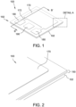
- FIG. 1 illustrates a perspective view of an example semiconductor assembly 100 in accordance with one or more embodiments of the present disclosure.
- FIG. 2 illustrates an enlarged view of Detail A of the semiconductor assembly 100
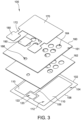
- FIG. 3 illustrates an exploded view of the semiconductor assembly 100
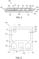
- FIG. 4 illustrates a cross-sectional view of the semiconductor assembly 100 taken along line B-B'.
- the semiconductor assembly 100 includes a POL-RDL package 150 disposed on a semiconductor device 102.
- the semiconductor device 102 includes a dielectric material 106 that defines an upper surface 104. An outer peripheral edge 108 of the dielectric material 106 defines a surface area of the semiconductor device 102.
- the semiconductor device 102 further includes at least one source pad 110 and a gate pad 120 disposed on the dielectric material 106.
- the at least one source pad 110 includes a top contact surface 112 and the gate pad 120 includes a top contact surface 122.
- the gate pad 120 and the at least one source pad 110 are spaced apart from each other on the dielectric material 106. As best shown in FIG.
- the gate pad 120 and the at least one source pad 110 are spaced from the outer peripheral edge 108 of the semiconductor device 102. In some embodiments, at least a portion of the gate pad 120 and the at least one source pad 110 extend below the upper surface 104. Further, in some embodiments, the top contact surface 112 of the at least one source pad 110 and the top contact surface 122 of the gate pad 120 are flush. The at least one source pad 110 is electrically isolated from adjacent source pads 110 on the semiconductor device 102.
- the at least one source pad 110 of the semiconductor device 102 is used for electricity control and conversion.
- the at least one source pad 110 may be configured to turn power received from the gate pad 120 on and off thousands of times per second.
- the POL-RDL package 150 may provide a bridging connection between the source pads 110.
- at least some known semiconductor devices include connections to external components as well as bridging connections between of source pads on the surface of the semiconductor device or on the surface of the source pads. Such connections limit available active surface area of the semiconductor device and may induce greater bonding stresses. As best shown in FIGS.
- the POL-RDL package 150 includes a dielectric layer 160 and an adhesive layer 162 positioned below the dielectric layer 160.
- the adhesive layer 162 includes dielectric material layer which adheres to the dielectric layer 160 and to the semiconductor device 102. That is, the adhesive layer 162 is positioned between the dielectric layer 160 and the semiconductor device 102.
- the dielectric layer 160 includes an adhesive material to adhere directly to the semiconductor device 102 without the use of the adhesive layer 162.
- the POL-RDL package 150 is positioned above the semiconductor device 102 and the dielectric layer 160 is adhered to the semiconductor device 102 by the adhesive layer 162.
- the dielectric layer 160 is in the form of a lamination or a film, and may be formed of one a plurality of dielectric materials, such as Kapton ® polyimide, Ultem ® polyetherimide, polytetrafluoroethylene (PTFE), Upilex ® , polysulfone materials (e.g., Udel ® polysulphone, Radel ® polyphenolsulphone), silica (SiO 2 ), hafnium silicate (HfSiO 4 ), zirconium silicate (ZrSiO 4 ) and barium titanate (BaTiO 3 ), or another polymer film, such as a liquid crystal polymer (LCP) or a polyimide material.
- the POL-RDL package 150 has a total thickness in the range of 25 microns to 300 micro
- At least one source pad 170, at least one contact pad 180, and a gate pad 190 are formed on an upper surface 161 of the dielectric layer 160.
- the at least one contact pad 180 is electrically coupled to the at least one source pad 170 by a trace connection 172 extending between the at least one contact pad 180 to the at least one source pad 170.
- the trace connection 172 has a resistance value different from a resistance value of the at least one contact pad 180.
- the trace connection 172 is made from a different material than the at least one contact pad 180.
- the trace connection 172 has a width smaller than a width of the at least one contact pad 180.
- the at least one contact pad 180 is a Kelvin gate contact.
- At least one source via pathway 164 and a gate via pathway 166 extend through the dielectric layer 160 and the adhesive layer 162.
- the POL-RDL package 150 also includes a metal interconnect structure 167 that extends through the least one source via pathway 164 and the gate via pathway 166.
- the metal interconnect structure 167 electrically couples the top contact surface 112 of the at least one source pad 110 of the semiconductor device 102 to the at least one source pad 170 of the POL-RDL package 150, and likewise electrically couples the top contact surface 122 of the gate pad 120 of the semiconductor device 102 to the gate pad 190 of the POL-RDL package 150.
- the metal interconnect structure 167 is formed by filling the at least one source via pathway 164 and the gate via pathway 166 with a conductive material (i.e., conductive epoxy, paste, or solder and the like). In some embodiments, the metal interconnect structure 167 is formed during deposition of the at least one source pad 170 and the gate pad 190. By way of example, as the at least one source pad 170 and the gate pad 190 are deposited, the at least one source via pathway 164 and the gate via pathway 166 are also filled. Subsequently the at least one source pad 170 and the gate pad 190 are electroplated to a desired thickness.
- a conductive material i.e., conductive epoxy, paste, or solder and the like.
- the at least one contact pad 180 is electrically coupled to the at least one source pad 170 such that the gate pad 190 establishes an input-output (I/O) connection with the source pad 170 and/or the at least one contact pad 180.
- the input-output (I/O) connection enables connection of the semiconductor device 102 to an external circuit, such as a printed circuit board (PCB).
- electrical connections include one or more of soldering, sintering, copper bonding, copper clipping and the like.
- electrical leads 101 can be attached to the gate pad 190, to the source pad 170, and to the least one contact pad 180. In such a configuration, the least one contact pad 180 is a Kelvin contact.
- a solder mask layer is applied over the at least one source pad 170 to provide a protective coating and define interconnect pads 171 for attaching of electrical leads 101 to the at least one source pad 170.
- the interconnect pads may have a metal finish to aid solderability, such as Ni, Cu, Ni/Au, Cu/Ni/Au, Cu/Ni/Pd/Au.
- the at least one contact pad 180, the source pad 170, and the gate pad 190 must have a sufficient surface area to make the electrical connection.
- the surface area of the at least one contact pad 180, the source pad 170, and the gate pad 190 is ultimately limited by the overall surface area of the dielectric layer 160.
- each of the at least one source pad 170, the at least one contact pad 180, and the gate pad 190 disposed on the dielectric layer 160 are positioned a distance from an outer peripheral edge 168 of the dielectric layer 160.
- each of the at least one source pad 170, the at least one contact pad 180, and the gate pad 190 disposed on the dielectric layer 160 should be spaced sufficiently far away from one another to isolate the components and prevent electrical leakage.
- the dielectric layer 160 has a surface area greater than a surface area of the semiconductor device 102 such that the outer peripheral edge 168 of the dielectric layer 160 extends beyond the outer peripheral edge 108 of the semiconductor device 102 to define an overhang region 174.
- the adhesive layer 162 extends to the outer peripheral edge 108 of the semiconductor device 102. In some embodiments, the adhesive layer 162 extends to the outer peripheral edge 168 of the dielectric layer 160. In some embodiments, the adhesive layer 162 extends partially to the outer peripheral edge 168 of the dielectric layer 160.
- the overhang region 174 allows the at least one contact pad 180, the source pad 170, and the gate pad 190 to have a larger surface area.
- any one of the at least one contact pad 180, the source pad 170, and the gate pad 190 extend to the outer peripheral edge 108 of the semiconductor device 102 as shown in FIG. 4 .
- the any one of the at least one contact pad 180, the source pad 170, and the gate pad 190 extend into the overhang region 174 and thus, any one of the at least one contact pad 180, the source pad 170, and the gate pad 190 extends beyond the outer peripheral edge 108 of the semiconductor device 102.
- overhang region 174 allows the source pad 170 and the gate pad 190 and the to have a larger surface area.
- the POL-RDL package 150 described herein allows for redistribution of the at least one contact pad 180 and the gate pad 120 on the dielectric layer 160, and allows for the at least one contact pad 180 and the gate pad 190 to have a greater surface area to facilitate easier and more robust connections to external circuitry.
- the POL-RDL package 150 also enables an improved elastic (Young's) modulus of the dielectric layer 160, which reduces bonding stress on the semiconductor device 102.
- the dielectric layer 160 of the POL-RDL package 150 may be polyimide, which has an elastic modulus of approximately 2.5 GPa, whereas the semiconductor device 102, which may be SiO 2 , may have an elastic modulus of approximately 70 GPa.
- the lower elastic modulus is capable of absorbing bonding stress, thereby reducing bonding stress on the semiconductor device 102.
- contact pads and gate pads in a POL package may have a surface area of up to 0.6 mm 2 without the benefit of the overhang region 174. Without the benefit of the additional surface area provided by the overhang region 174, a larger gate pad would necessarily reduce the available area for placement of a source pad and contact pad in the semiconductor device 102, resulting in a lower current rating of the semiconductor device 102.
- the at least one contact pad 180 given the benefit of the overhang region 174, has a surface area in the range of 0.5mm 2 to 1.5mm 2 while still maintaining the current rating of the semiconductor device 102. In some embodiments, the surface area of the contact pads 180 is greater than 0.6mm 2 .
- the overhang region 174 of the POL-RDL package 150 allows for redistribution of the at least one contact pad 180 and the gate pad 190 while still maintaining the current rating of the semiconductor device 102. Similar to the at least one contact pad 180, the source pad 170 and the gate pad 190 can also have a greater surface area.
- the overhang region 174 and greater surface area of the POL-RDL package 150 also facilitate using a wide range of trace connections 172 with varying resistivity values (as shown in FIGS. 8-11 ).
- Using different types of trace configurations 172 enables selectively tuning of the resistivity value between the source pad 110 and the at least one contact pad 180.
- additional resistance between the at least one source pad 110 and the at least one contact pad 180 reduces crosstalk, thus improving efficiency of the semiconductor device 102.
- the resistance value between the at least one source pad 110 and the at least one contact pad 180 can be selectively adjusted for specific applications without altering the semiconductor device 102 during fabrication and assembly. This allows for simplified fabrication of a base semiconductor device 102 with post-fabrication customization of the trace connections 172 depending on specific customer and application needs.
- the resistivity value of the trace connection 172 can be altered by depositing the trace connection 172 with material having different resistivities, by modifying a width of the trace connection 172, and/or by modifying a deposition thickness of the trace connection 172.
- An exemplary trace connection 172 having a length of 2mm, a width of 35mm and a thickness of 10mm has a resistance of approximately 0.1 Q.
- the trace connection 172 has a thickness in the range of 5-25mm, and a trace width of approximately 25mm.
- the trace connection 172 deposition depth in a range from 50 nm to 50 ⁇ m.
- the resistivity value of the trace connections 172 is tuned or altered by changing the volume of the trace connection 172, changing the cross-sectional area of the trace connection 172, and/or changing the material of the trace connection 172.
- the trace connection 172 is made from a combination of a first material having a first resistivity value and a second material having a second resistivity value, and the second material is laminated or otherwise layered over the first material.
- the resistivity value of the trace connection 172 may be selectively adjustable within a range of 10mQ (micro-ohms) to 100m ⁇ .
- the trace connection 172 is a resistor. Further, in some embodiments, the trace connection 172 is a surface-mounted resistor.
- the at least one contact pad 180 and the at least one source pad 170 include attachment pads 178.
- the trace connection 172 is implemented as a surface-mounted a resistor 176 coupled between the attachment pads 178.
- the resistor 176 can be connected to the semiconductor assembly 100 post-fabrication.
- FIG. 7 illustrates a method 200 of manufacturing a semiconductor assembly, such as the semiconductor assembly 100 (shown in FIGS. 1-6 ).
- the method 200 includes adhering 202 a dielectric layer of a POL-RDL package to an upper surface of a semiconductor device in a panel format, filling 204 at least one source via pathway defined in the dielectric layer with at least one metallization via, and depositing 206 at least one source pad and at least one contact pad onto an upper surface of the dielectric layer.
- the method 200 further includes depositing a trace connection having a resistivity value between the at least one source pad and the at least one contact pad.
- the method 200 further includes forming solder pads on the at least one source pad and the at least one contact pad of the dielectric layer, and soldering a resistor onto the solder pads.
- the trace connection is formed by sputtering or depositing a resistive material such as Tantalum nitride (TaN) between the at least one source pad and the at least one contact pad
- the method 200 further includes forming 208 a copper connection to a top surface of the at least one contact pad to connect the semiconductor assembly to external circuitry
- the metallization vias are formed by laser ablation or laser drilling process, plasma etching, photo-definition, and/or mechanical drilling or punching processes. Furthermore, a combination of pre-and post-drilled vias could be employed.
- the metallization layer is formed through a combination of sputtering and electroplating applications, although it is recognized that other electroless methods of metal deposition could also be used.
- a titanium adhesion layer and a copper seed layer may first be applied via a sputtering process, followed by an electroplating process that increases a thickness of the copper to a desired level.
- the applied metal material is then subsequently patterned into metal interconnects having a desired shape and that function as vertical feed-throughs formed through the dielectric layer and the adhesive layer.
- FIGS. 8 and 9 additional alternative embodiments of the configuration of at least one source pad, the gate pad, and the at least one contact pad on the POL-RDL package are illustrated.
- the semiconductor assembly shown in FIGS. 8 and 9 includes a number of components similar to components shown in semiconductor assembly 100 of FIG. 1 .
- FIG. 8 illustrates a perspective view of one embodiment of a semiconductor assembly 300 including a source pad 370, a contact pad 380 and a gate pad 390 positioned on a dielectric layer 360.
- FIG. 9 illustrates a top view of the semiconductor assembly 300, with the components of the semiconductor device 102 shown in dashed lines.
- the source pad 370 and contact pad 380 are integral with one another, with no discrete trace connection extending between the source pad 370 and the contact pad 380.
- the gate pad 390 has a surface area greater than a surface area of the gate pad 190 of FIG. 1 .
- the gate pad 120 of the semiconductor device 102 is vertically aligned with a portion of the gate pad 390 and the source pads 110 of the semiconductor device 102 are vertically aligned with portions of the source pad 370 to facilitate connections between those components.
- the source pad 370, a contact pad 380, and a gate pad 390 extend into the overhang region 174.
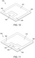
- FIG. 10 shows another embodiment of a semiconductor assembly 400 including a source pad 570, two contact pads 480, and a gate pad 490 positioned on a dielectric layer 460.
- the source pad 470 and two contact pads 480 are integral, without discrete trace connections extending between the source pad 470 and the two contact pads 480.
- FIG. 11 shows another embodiment of a semiconductor assembly 500 including a source pad 570, a contact pad 580, and a gate pad 590 positioned on a dielectric layer 560.
- the source pad 570 and contact pad 580 are integral, without a discrete trace connection extending between the source pad 570 and the contact pad 580.
- a metallization via connects a gate pad of the semiconductor device to a gate contact 594 on the dielectric layer 560.
- the gate contact 594 is vertically aligned with the underlying gate pad.
- a trace connection 592 connects the gate contact 594 to the gate pad 590.
- the trace connection 592 has a resistivity value different from a resistivity value of the gate pad 590.
- the trace connection 592 is made from a different material from the gate pad 590. In some embodiments, the trace connection 592 has a width smaller than a width of the gate pad 590.Further, in these embodiments, any of the contact pads (380, 480, 580) may have a different surface finish than that of the source pad (370, 470, 570).
- the configurations of the embodiments of FIGS. 8 - 11 are optimized for GENERAL ELECTRIC ® semiconductor devices, however the configurations can be optimized for other semiconductor devices.
- the above-described embodiments overcome at least some disadvantages of semiconductor devices.
- the embodiments described herein facilitate redistribution of the contact pads and the gate pad on the dielectric layer, and allow for the contact pads and the gate pad to have a greater surface area for an easier and more robust connections to external circuitry.
- the POL-RDL package described herein also provides an improved elastic modulus of the dielectric layer, which reduces bonding stress on the semiconductor device.
- the oversized POL-RDL package also allows for redistribution of the contact pads and the gate pad while still maintaining the current rating of the semiconductor device.
- the greater surface area of the POL-RDL package described herein also facilitates using a variety of trace connections with varying resistivity values.
- the resistivity values of the trace configurations may be selectively adjusted to control the resistivity value between the source pad and the contact pad. Added resistance generally reduces crosstalk, thus improving efficiency of the semiconductor device.
- a semiconductor assembly including: a semiconductor device including: an upper surface; a gate pad disposed on said upper surface; and at least one source pad disposed on said upper surface; and a POL-RDL package coupled to said semiconductor device and including: a dielectric layer including an upper surface; at least one source pad disposed on said upper surface of said dielectric layer and electrically coupled to said at least one source pad of said semiconductor device; at least one contact pad disposed on said upper surface of said dielectric layer; and at least one trace connection having a resistivity value and electrically coupling said at least one source pad of said POL-RDL package to said at least one contact pad.
- the semiconductor assembly of any of the preceding clause further including a gate pad disposed on said upper surface of said dielectric layer and electrically coupled to said gate pad of said semiconductor device.
- said at least one trace connection has a width less than a width of said at least one contact pad, and wherein the width of said trace connection controls the resistivity value of said trace connection.
- said at least one trace connection is made from a first material having a first resistivity value and said at least one contact pad is made from a material having a second resistivity value, and wherein said first resistivity value is greater than said second resistivity value.
- the semiconductor assembly of any of the preceding clause further including at least one interconnect pad for attaching of electrical leads to said at least one source pad.
- said at least one trace connection includes a resistor mounted to said attachment pads with solder.
- said semiconductor device includes a first outer peripheral edge that defines a first surface area
- said dielectric layer of said POL-RDL package includes a second outer peripheral edge that defines a second surface area, wherein the second surface area is greater than the first surface area, and wherein said second outer peripheral edge extends beyond said first outer peripheral edge to define an overhang region.
- said POL-RDL package further includes a gate contact disposed on said dielectric layer; and an additional trace connection electrically coupling said gate contact to said gate pad of said semiconductor device.
- a method of manufacturing a semiconductor assembly including: coupling a dielectric layer of a POL-RDL package to an upper surface of a semiconductor device, the semiconductor device including at least one source pad and a gate pad disposed on the upper surface; forming at least one source pad of the POL-RDL package on an upper surface of the dielectric layer; electrically coupling the at least one source pad of the POL-RDL package to the at least one source pad of the semiconductor device; forming a gate pad of the POL-RDL package on the upper surface of the dielectric layer; electrically coupling the gate pad of the POL-RDL package to the gate pad of the semiconductor device; forming at least one contact pad on the upper surface of the dielectric layer; and electrically coupling the at least one source pad of the POL-RDL package to the at least one contact pad using at least one trace connection having a resistivity value.
- the semiconductor device includes a first outer peripheral edge that defines a first surface area
- the dielectric layer of the POL-RDL package includes a second outer peripheral edge that defines a second surface area, wherein the second surface area is greater than the first surface area, and wherein the second outer peripheral edge extends beyond the first outer peripheral edge to define an overhang region.
- the at least one trace connection has a width less than a width of the at least one contact pad, and wherein the width of the trace connection controls the resistivity value of the trace connection.
Landscapes
- Internal Circuitry In Semiconductor Integrated Circuit Devices (AREA)
- Physics & Mathematics (AREA)
- Geometry (AREA)
- Engineering & Computer Science (AREA)
- Manufacturing & Machinery (AREA)
Abstract
Description
- The present disclosure relates generally to semiconductor devices, and more particularly to semiconductor devices having a power overlay package.
- Power semiconductor assemblies include devices used as switches or rectifiers in power electronic circuits, such as switched mode power supplies and the like. Power semiconductor devices are used in high voltage power applications to carry large amounts of current and to support large voltages. In use, high voltage power semiconductor devices are connected to an external circuit by way of power overlay ("POL") packages and an interconnect system.
- In at least some known assemblies, a POL package is layered onto a semiconductor device. The semiconductor device includes at least one source pad and a gate pad disposed on a top surface of the semiconductor device. The POL package includes at least one POL interconnect layer configured as a routing layer. The at least one POL interconnect layer is laminated with at least one dielectric layer (also referred to as an isolation film) deposited on the semiconductor device, and metallization vias extending through the dielectric layer. The metallization vias electrically couple the at least one source pad of the semiconductor device to a source pad disposed on a top surface of the dielectric layer, while a gate pad disposed on the top surface of the dielectric layer is coupled to the gate pad of the semiconductor device. A contact pad (such as a Kelvin contact) disposed on the top surface of the dielectric layer is electrically coupled to the source pad of the dielectric layer.
- POL packages generally utilize connections to electrically couple to the source pad, to the contact pad, and to the gate pad on the dielectric layer to deliver power to the semiconductor device through the metallization vias. To establish a proper electrical connection, the source pad, the contact pad, and the gate pad on the dielectric layer require sufficient surface area to solder, sinter, copper bond, copper clip, or otherwise connect the source pad, the contact pad, and the gate pad with the connections. However, the surface areas of the source pad, the contact pad, and the gate pad are generally limited by the overall surface area of the semiconductor device. Further, direct soldering, sintering, copper bonding, and copper clipping to the source pad and the gate pad on the semiconductor device, without a POL package, introduces bonding stresses onto the semiconductor device. The introduction of the source pad, the contact pad, and the gate pad on the dielectric layer of the POL package provides stress buffering and reduces the stress on to the semiconductor device.
- Therefore, there is a need to improve available surface of the POL package such that larger source pads, contact pads and gate pads can be utilized while not reducing available active area of the semiconductor devices, and to reduce bonding stress of the bonding connections to the semiconductor device surface.
- In one aspect, a semiconductor assembly including a semiconductor device and a POL-RDL package coupled to said semiconductor device is disclosed. The device includes an upper surface, a gate pad disposed on said upper surface; and at least one source pad disposed on said upper surface. The POL-RDL package includes a dielectric layer comprising an upper surface, at least one source pad disposed on said upper surface of said dielectric layer and electrically coupled to said at least one source pad of said semiconductor device; at least one contact pad disposed on said upper surface of said dielectric layer; and at least one trace connection having a resistivity value and electrically coupling said at least one source pad of said POL-RDL package to said at least one contact pad.
- In another aspect, method of manufacturing a semiconductor assembly is disclosed. The method includes coupling a dielectric layer of a POL-RDL package to an upper surface of a semiconductor device, the semiconductor device including at least one source pad and a gate pad disposed on the upper surface; forming at least one source pad of the POL-RDL package on an upper surface of the dielectric layer; electrically coupling the at least one source pad of the POL-RDL package to the at least one source pad of the semiconductor device; forming a gate pad of the POL-RDL package on the upper surface of the dielectric layer; electrically coupling the gate pad of the POL-RDL package to the gate pad of the semiconductor device; forming at least one contact pad on the upper surface of the dielectric layer; and electrically coupling the at least one source pad of the POL-RDL package to the at least one contact pad using at least one trace connection having a resistivity value.
- The subject-matter of the disclosure will be explained in more detail in the following text with reference to exemplary embodiments which are illustrated in the attached drawings.
-
FIG. 1 is a perspective view of a semiconductor assembly including a POL package disposed on a semiconductor device in accordance with one or more embodiments of the present disclosure. -
FIG. 2 is an enlarged view of Detail A of the semiconductor assembly ofFIG. 1 ; -
FIG. 3 is an exploded view of the semiconductor assembly ofFIG. 1 ; -
FIG. 4 is a cross-sectional view of the semiconductor assembly ofFIG. 1 taken along line B-B'; -
FIG. 5 is a top view of the semiconductor assembly ofFIG. 1 ; -
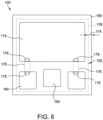
FIG. 6 is a top view of one embodiment of the semiconductor assembly ofFIG. 1 . -
FIG. 7 illustrates one embodiment of a method of manufacturing a semiconductor assembly; -
FIG. 8 is perspective view of an alternative embodiment of a semiconductor assembly; -
FIG. 9 is a top view of the semiconductor assembly shown inFIG. 8 , with the semiconductor device shown in dashed lines; and -
FIGS. 10 and 11 are perspective views of alternative embodiments of a semiconductor assembly. - The reference symbols used in the drawings, and their meanings, are listed in summary form in the list of reference symbols. In principle, identical parts are provided with the same reference symbols in the figures.
- In the following specification and the claims, reference will be made to a number of terms, which shall be defined to have the following meanings.
- As used herein, the singular forms "a," "an," and "the" include plural references unless the context clearly dictates otherwise. The terms "comprising," "including," and "having" are intended to be inclusive and mean that there may be additional elements other than the listed elements. The terms "optional" or "optionally" means that the subsequently described event or circumstance may or may not occur, and that the description includes instances where the event occurs and instances where it does not.
- Unless otherwise indicated, approximating language, such as "generally," "substantially," and "about," as used herein indicates that the term so modified may apply to only an approximate degree, as would be recognized by one of ordinary skill in the art, rather than to an absolute or perfect degree. Accordingly, a value modified by a term or terms, such as "about," "approximately," and "substantially," is not to be limited to the precise value specified. In at least some instances, the approximating language may correspond to the precision of an instrument for measuring the value. Here and throughout the specification and claims, range limitations may be identified. Such ranges may be combined and/or interchanged, and include all the sub-ranges contained therein unless context or language indicates otherwise.
- Additionally, unless otherwise indicated, the terms "first," "second," etc. are used herein merely as labels, and are not intended to impose ordinal, positional, or hierarchical requirements on the items to which these terms refer. Moreover, reference to, for example, a "second" item does not require or preclude the existence of, for example, a "first" or lower-numbered item or a "third" or higher-numbered item.
- Embodiments of the disclosure relate generally to structures and methods for packaging semiconductor devices and, more particularly, to semiconductor devices including an overhanging POL structure. The methods, systems, and apparatus described herein overcome at least some disadvantages of at least some known power semiconductor devices having POL packages. More specifically, the systems and apparatus described herein provide a POL package configured as a redistribution layer (RDL) positioned directly over a power semiconductor device. Accordingly, the POL package is also referred to herein as a POL-RDL package. The POL-RDL package includes an oversized surface area relative to the semiconductor device, which improves available surface area for placement of a source pad, a gate pad, and a contact pad on a top surface of the POL-RDL package. The improved available surface area allows for the use of larger source pads, contact pads, and gate pads, which reduce bonding stress on the semiconductor device. Furthermore, the improved available surface area allows for use of various trace configurations for POL-RDL packages.
- A semiconductor assembly including a semiconductor device and a POL-RDL package configured as a redistribution layer for the semiconductor device is disclosed. The semiconductor device includes at least one source pad and a gate pad disposed on a die having a surface area and an outer peripheral edge. The POL-RDL package includes a dielectric layer and an adhesive layer that is in contact with the semiconductor device. At least one source pad, a gate pad, and at least contact pad of the POL-RDL package are positioned on an upper surface of the dielectric layer. At least one source via pathway and a gate via pathway extend through the dielectric layer and the adhesive layer, and metallization vias are formed within the via pathways to connect the gate pad and the at least one source pad of the semiconductor device to the gate pad and the at least one source pad of the POL-RDL package, respectively. The POL-RDL package, and in particular the dielectric layer of the POL-RDL package, has an outer peripheral edge and a surface area greater than the surface area of the semiconductor device such that the outer peripheral edge of the dielectric layer extends beyond the outer peripheral edge of the semiconductor device, defining an overhang region. The larger surface area of the POL-RDL package increases available surface area for the sizes and positions of the gate pad, the at least one source pad, and the at least one contact pad of the POL-RDL package. This allows for greater flexibility in the use of traces connecting the at least one contact pad to the at least one source pad of the POL-RDL package, as described herein.
-
FIG. 1 illustrates a perspective view of anexample semiconductor assembly 100 in accordance with one or more embodiments of the present disclosure.FIG. 2 illustrates an enlarged view of Detail A of thesemiconductor assembly 100,FIG. 3 illustrates an exploded view of thesemiconductor assembly 100, andFIG. 4 illustrates a cross-sectional view of thesemiconductor assembly 100 taken along line B-B'. - As shown in
FIGS. 1 through 4 , thesemiconductor assembly 100 includes a POL-RDL package 150 disposed on asemiconductor device 102. As best shown inFIGS. 3 and4 , thesemiconductor device 102 includes adielectric material 106 that defines anupper surface 104. An outerperipheral edge 108 of thedielectric material 106 defines a surface area of thesemiconductor device 102. Thesemiconductor device 102 further includes at least onesource pad 110 and agate pad 120 disposed on thedielectric material 106. The at least onesource pad 110 includes atop contact surface 112 and thegate pad 120 includes atop contact surface 122. Thegate pad 120 and the at least onesource pad 110 are spaced apart from each other on thedielectric material 106. As best shown inFIG. 3 , thegate pad 120 and the at least onesource pad 110 are spaced from the outerperipheral edge 108 of thesemiconductor device 102. In some embodiments, at least a portion of thegate pad 120 and the at least onesource pad 110 extend below theupper surface 104. Further, in some embodiments, thetop contact surface 112 of the at least onesource pad 110 and thetop contact surface 122 of thegate pad 120 are flush. The at least onesource pad 110 is electrically isolated fromadjacent source pads 110 on thesemiconductor device 102. - The at least one
source pad 110 of thesemiconductor device 102 is used for electricity control and conversion. By way of example, the at least onesource pad 110 may be configured to turn power received from thegate pad 120 on and off thousands of times per second. In embodiments includingmultiple source pads 110, the POL-RDL package 150 may provide a bridging connection between thesource pads 110. Unlike the semiconductor assemblies of the present disclosure, at least some known semiconductor devices include connections to external components as well as bridging connections between of source pads on the surface of the semiconductor device or on the surface of the source pads. Such connections limit available active surface area of the semiconductor device and may induce greater bonding stresses. As best shown inFIGS. 1 through 3 , the POL-RDL package 150 includes adielectric layer 160 and anadhesive layer 162 positioned below thedielectric layer 160. Theadhesive layer 162 includes dielectric material layer which adheres to thedielectric layer 160 and to thesemiconductor device 102. That is, theadhesive layer 162 is positioned between thedielectric layer 160 and thesemiconductor device 102. In some embodiments, thedielectric layer 160 includes an adhesive material to adhere directly to thesemiconductor device 102 without the use of theadhesive layer 162. - The POL-
RDL package 150 is positioned above thesemiconductor device 102 and thedielectric layer 160 is adhered to thesemiconductor device 102 by theadhesive layer 162. In some embodiments, thedielectric layer 160 is in the form of a lamination or a film, and may be formed of one a plurality of dielectric materials, such as Kapton® polyimide, Ultem® polyetherimide, polytetrafluoroethylene (PTFE), Upilex®, polysulfone materials (e.g., Udel® polysulphone, Radel® polyphenolsulphone), silica (SiO2), hafnium silicate (HfSiO4), zirconium silicate (ZrSiO4) and barium titanate (BaTiO3), or another polymer film, such as a liquid crystal polymer (LCP) or a polyimide material. In one embodiment, the POL-RDL package 150 has a total thickness in the range of 25 microns to 300 microns - At least one
source pad 170, at least onecontact pad 180, and agate pad 190 are formed on anupper surface 161 of thedielectric layer 160. In this embodiment, the at least onecontact pad 180 is electrically coupled to the at least onesource pad 170 by atrace connection 172 extending between the at least onecontact pad 180 to the at least onesource pad 170. Thetrace connection 172 has a resistance value different from a resistance value of the at least onecontact pad 180. In some embodiments, to achieve the different resistivity values, thetrace connection 172 is made from a different material than the at least onecontact pad 180. Additionally or alternatively, in some embodiments, to achieve the different resistivity values, thetrace connection 172 has a width smaller than a width of the at least onecontact pad 180. In some embodiments, the at least onecontact pad 180 is a Kelvin gate contact. - At least one source via
pathway 164 and a gate viapathway 166 extend through thedielectric layer 160 and theadhesive layer 162. As best shown inFIG. 4 , the POL-RDL package 150 also includes ametal interconnect structure 167 that extends through the least one source viapathway 164 and the gate viapathway 166. Themetal interconnect structure 167 electrically couples thetop contact surface 112 of the at least onesource pad 110 of thesemiconductor device 102 to the at least onesource pad 170 of the POL-RDL package 150, and likewise electrically couples thetop contact surface 122 of thegate pad 120 of thesemiconductor device 102 to thegate pad 190 of the POL-RDL package 150. - In some embodiments, the
metal interconnect structure 167 is formed by filling the at least one source viapathway 164 and the gate viapathway 166 with a conductive material (i.e., conductive epoxy, paste, or solder and the like). In some embodiments, themetal interconnect structure 167 is formed during deposition of the at least onesource pad 170 and thegate pad 190. By way of example, as the at least onesource pad 170 and thegate pad 190 are deposited, the at least one source viapathway 164 and the gate viapathway 166 are also filled. Subsequently the at least onesource pad 170 and thegate pad 190 are electroplated to a desired thickness. - The at least one
contact pad 180 is electrically coupled to the at least onesource pad 170 such that thegate pad 190 establishes an input-output (I/O) connection with thesource pad 170 and/or the at least onecontact pad 180. The input-output (I/O) connection enables connection of thesemiconductor device 102 to an external circuit, such as a printed circuit board (PCB). In some embodiments, electrical connections include one or more of soldering, sintering, copper bonding, copper clipping and the like. By way of example, as shown inFIG. 5 ,electrical leads 101 can be attached to thegate pad 190, to thesource pad 170, and to the least onecontact pad 180. In such a configuration, the least onecontact pad 180 is a Kelvin contact. In some embodiments, a solder mask layer is applied over the at least onesource pad 170 to provide a protective coating and defineinterconnect pads 171 for attaching ofelectrical leads 101 to the at least onesource pad 170. In an alternative embodiment, the interconnect pads may have a metal finish to aid solderability, such as Ni, Cu, Ni/Au, Cu/Ni/Au, Cu/Ni/Pd/Au. - To establish a proper connection, the at least one
contact pad 180, thesource pad 170, and thegate pad 190 must have a sufficient surface area to make the electrical connection. However, the surface area of the at least onecontact pad 180, thesource pad 170, and thegate pad 190 is ultimately limited by the overall surface area of thedielectric layer 160. By way of example, each of the at least onesource pad 170, the at least onecontact pad 180, and thegate pad 190 disposed on thedielectric layer 160 are positioned a distance from an outerperipheral edge 168 of thedielectric layer 160. Furthermore, each of the at least onesource pad 170, the at least onecontact pad 180, and thegate pad 190 disposed on thedielectric layer 160 should be spaced sufficiently far away from one another to isolate the components and prevent electrical leakage. - As best shown in
FIGS. 2 ,4 and 5 , thedielectric layer 160 has a surface area greater than a surface area of thesemiconductor device 102 such that the outerperipheral edge 168 of thedielectric layer 160 extends beyond the outerperipheral edge 108 of thesemiconductor device 102 to define anoverhang region 174. In some embodiments, theadhesive layer 162 extends to the outerperipheral edge 108 of thesemiconductor device 102. In some embodiments, theadhesive layer 162 extends to the outerperipheral edge 168 of thedielectric layer 160. In some embodiments, theadhesive layer 162 extends partially to the outerperipheral edge 168 of thedielectric layer 160. - The
overhang region 174 allows the at least onecontact pad 180, thesource pad 170, and thegate pad 190 to have a larger surface area. In particular, in some embodiments, any one of the at least onecontact pad 180, thesource pad 170, and thegate pad 190 extend to the outerperipheral edge 108 of thesemiconductor device 102 as shown inFIG. 4 . In some embodiments, the any one of the at least onecontact pad 180, thesource pad 170, and thegate pad 190 extend into theoverhang region 174 and thus, any one of the at least onecontact pad 180, thesource pad 170, and thegate pad 190 extends beyond the outerperipheral edge 108 of thesemiconductor device 102. Similar to the least onecontact pad 180,overhang region 174 allows thesource pad 170 and thegate pad 190 and the to have a larger surface area. - The POL-
RDL package 150 described herein allows for redistribution of the at least onecontact pad 180 and thegate pad 120 on thedielectric layer 160, and allows for the at least onecontact pad 180 and thegate pad 190 to have a greater surface area to facilitate easier and more robust connections to external circuitry. The POL-RDL package 150 also enables an improved elastic (Young's) modulus of thedielectric layer 160, which reduces bonding stress on thesemiconductor device 102. Thedielectric layer 160 of the POL-RDL package 150 may be polyimide, which has an elastic modulus of approximately 2.5 GPa, whereas thesemiconductor device 102, which may be SiO2, may have an elastic modulus of approximately 70 GPa. The lower elastic modulus is capable of absorbing bonding stress, thereby reducing bonding stress on thesemiconductor device 102. - In at least some known semiconductor assemblies, contact pads and gate pads in a POL package may have a surface area of up to 0.6 mm2 without the benefit of the
overhang region 174. Without the benefit of the additional surface area provided by theoverhang region 174, a larger gate pad would necessarily reduce the available area for placement of a source pad and contact pad in thesemiconductor device 102, resulting in a lower current rating of thesemiconductor device 102. - In contrast, in at least some of the embodiments described herein, the at least one
contact pad 180, given the benefit of theoverhang region 174, has a surface area in the range of 0.5mm2 to 1.5mm2 while still maintaining the current rating of thesemiconductor device 102. In some embodiments, the surface area of thecontact pads 180 is greater than 0.6mm2. Thus, theoverhang region 174 of the POL-RDL package 150 allows for redistribution of the at least onecontact pad 180 and thegate pad 190 while still maintaining the current rating of thesemiconductor device 102. Similar to the at least onecontact pad 180, thesource pad 170 and thegate pad 190 can also have a greater surface area. - The
overhang region 174 and greater surface area of the POL-RDL package 150 also facilitate using a wide range oftrace connections 172 with varying resistivity values (as shown inFIGS. 8-11 ). Using different types oftrace configurations 172 enables selectively tuning of the resistivity value between thesource pad 110 and the at least onecontact pad 180. Notably, additional resistance between the at least onesource pad 110 and the at least onecontact pad 180 reduces crosstalk, thus improving efficiency of thesemiconductor device 102. In accordance with the embodiments described herein, the resistance value between the at least onesource pad 110 and the at least onecontact pad 180 can be selectively adjusted for specific applications without altering thesemiconductor device 102 during fabrication and assembly. This allows for simplified fabrication of abase semiconductor device 102 with post-fabrication customization of thetrace connections 172 depending on specific customer and application needs. - For example, the resistivity value of the
trace connection 172 can be altered by depositing thetrace connection 172 with material having different resistivities, by modifying a width of thetrace connection 172, and/or by modifying a deposition thickness of thetrace connection 172. Anexemplary trace connection 172 having a length of 2mm, a width of 35mm and a thickness of 10mm has a resistance of approximately 0.1 Q. In some embodiments, thetrace connection 172 has a thickness in the range of 5-25mm, and a trace width of approximately 25mm. In some embodiments, thetrace connection 172 deposition depth in a range from 50 nm to 50 µm. In some embodiments, the resistivity value of thetrace connections 172 is tuned or altered by changing the volume of thetrace connection 172, changing the cross-sectional area of thetrace connection 172, and/or changing the material of thetrace connection 172. In some embodiments, thetrace connection 172 is made from a combination of a first material having a first resistivity value and a second material having a second resistivity value, and the second material is laminated or otherwise layered over the first material. The resistivity value of thetrace connection 172 may be selectively adjustable within a range of 10mQ (micro-ohms) to 100mΩ. In some embodiments, thetrace connection 172 is a resistor. Further, in some embodiments, thetrace connection 172 is a surface-mounted resistor. - As shown in
FIG. 6 , in some embodiments, the at least onecontact pad 180 and the at least onesource pad 170 includeattachment pads 178. In such embodiments, thetrace connection 172 is implemented as a surface-mounted aresistor 176 coupled between theattachment pads 178. Theresistor 176 can be connected to thesemiconductor assembly 100 post-fabrication. -
FIG. 7 illustrates amethod 200 of manufacturing a semiconductor assembly, such as the semiconductor assembly 100 (shown inFIGS. 1-6 ). Themethod 200 includes adhering 202 a dielectric layer of a POL-RDL package to an upper surface of a semiconductor device in a panel format, filling 204 at least one source via pathway defined in the dielectric layer with at least one metallization via, and depositing 206 at least one source pad and at least one contact pad onto an upper surface of the dielectric layer. In some embodiments, themethod 200 further includes depositing a trace connection having a resistivity value between the at least one source pad and the at least one contact pad. In some embodiments, themethod 200 further includes forming solder pads on the at least one source pad and the at least one contact pad of the dielectric layer, and soldering a resistor onto the solder pads. - In some embodiments, the trace connection is formed by sputtering or depositing a resistive material such as Tantalum nitride (TaN) between the at least one source pad and the at least one contact pad In some embodiments, the
method 200 further includes forming 208 a copper connection to a top surface of the at least one contact pad to connect the semiconductor assembly to external circuitry In some embodiments, the metallization vias are formed by laser ablation or laser drilling process, plasma etching, photo-definition, and/or mechanical drilling or punching processes. Furthermore, a combination of pre-and post-drilled vias could be employed. - In some embodiments, the metallization layer is formed through a combination of sputtering and electroplating applications, although it is recognized that other electroless methods of metal deposition could also be used. For example, a titanium adhesion layer and a copper seed layer may first be applied via a sputtering process, followed by an electroplating process that increases a thickness of the copper to a desired level. The applied metal material is then subsequently patterned into metal interconnects having a desired shape and that function as vertical feed-throughs formed through the dielectric layer and the adhesive layer.
- Referring now to
FIGS. 8 and 9 , additional alternative embodiments of the configuration of at least one source pad, the gate pad, and the at least one contact pad on the POL-RDL package are illustrated. The semiconductor assembly shown inFIGS. 8 and 9 includes a number of components similar to components shown insemiconductor assembly 100 ofFIG. 1 . - More specifically,
FIG. 8 illustrates a perspective view of one embodiment of asemiconductor assembly 300 including asource pad 370, acontact pad 380 and agate pad 390 positioned on adielectric layer 360.FIG. 9 illustrates a top view of thesemiconductor assembly 300, with the components of thesemiconductor device 102 shown in dashed lines. As shown inFIG. 8 , thesource pad 370 andcontact pad 380 are integral with one another, with no discrete trace connection extending between thesource pad 370 and thecontact pad 380. Thegate pad 390 has a surface area greater than a surface area of thegate pad 190 ofFIG. 1 . Furthermore, in the illustrated embodiment, there is only onecontact pad 380. As shown inFIG. 9 , thegate pad 120 of thesemiconductor device 102 is vertically aligned with a portion of thegate pad 390 and thesource pads 110 of thesemiconductor device 102 are vertically aligned with portions of thesource pad 370 to facilitate connections between those components. In some embodiments, thesource pad 370, acontact pad 380, and agate pad 390 extend into theoverhang region 174. -
FIG. 10 shows another embodiment of asemiconductor assembly 400 including asource pad 570, twocontact pads 480, and agate pad 490 positioned on adielectric layer 460. Thesource pad 470 and twocontact pads 480 are integral, without discrete trace connections extending between thesource pad 470 and the twocontact pads 480. -
FIG. 11 shows another embodiment of asemiconductor assembly 500 including asource pad 570, acontact pad 580, and agate pad 590 positioned on adielectric layer 560. Thesource pad 570 andcontact pad 580 are integral, without a discrete trace connection extending between thesource pad 570 and thecontact pad 580. In this embodiment, a metallization via connects a gate pad of the semiconductor device to agate contact 594 on thedielectric layer 560. Thegate contact 594 is vertically aligned with the underlying gate pad. Further, atrace connection 592 connects thegate contact 594 to thegate pad 590. In some embodiments, thetrace connection 592 has a resistivity value different from a resistivity value of thegate pad 590. In some embodiments, thetrace connection 592 is made from a different material from thegate pad 590. In some embodiments, thetrace connection 592 has a width smaller than a width of the gate pad 590.Further, in these embodiments, any of the contact pads (380, 480, 580) may have a different surface finish than that of the source pad (370, 470, 570). By way of example, the configurations of the embodiments ofFIGS. 8 - 11 are optimized for GENERAL ELECTRIC® semiconductor devices, however the configurations can be optimized for other semiconductor devices. - The above-described embodiments overcome at least some disadvantages of semiconductor devices. Specifically, the embodiments described herein facilitate redistribution of the contact pads and the gate pad on the dielectric layer, and allow for the contact pads and the gate pad to have a greater surface area for an easier and more robust connections to external circuitry. The POL-RDL package described herein also provides an improved elastic modulus of the dielectric layer, which reduces bonding stress on the semiconductor device. The oversized POL-RDL package also allows for redistribution of the contact pads and the gate pad while still maintaining the current rating of the semiconductor device.
- The greater surface area of the POL-RDL package described herein also facilitates using a variety of trace connections with varying resistivity values. The resistivity values of the trace configurations may be selectively adjusted to control the resistivity value between the source pad and the contact pad. Added resistance generally reduces crosstalk, thus improving efficiency of the semiconductor device.
- The methods, systems, and compositions disclosed herein are not limited to the specific embodiments described herein, but rather, steps of the methods, elements of the systems, and/or elements of the compositions may be utilized independently and separately from other steps and/or elements described herein.
- Although specific features of various embodiments may be shown in some drawings and not in others, this is for convenience only. Moreover, references to "one embodiment" in the above description are not intended to be interpreted as excluding the existence of additional embodiments that also incorporate the recited features. In accordance with the principles of the disclosure, any feature of a drawing may be referenced and/or claimed in combination with any feature of any other drawing.
- This written description uses examples, including the best mode, to enable any person skilled in the art to practice the disclosure, including making and using any devices or systems and performing any incorporated methods. The patentable scope of the disclosure is defined by the claims, and may include other examples that occur to those skilled in the art. Such other examples are intended to be within the scope of the claims if they have structural elements that do not differ from the literal language of the claims, or if they include equivalent structural elements with insubstantial differences from the literal languages of the claims.
- Further aspects of the disclosure are provided by the subject matter of the following clauses:
- A semiconductor assembly including: a semiconductor device including: an upper surface; a gate pad disposed on said upper surface; and at least one source pad disposed on said upper surface; and a POL-RDL package coupled to said semiconductor device and including: a dielectric layer including an upper surface; at least one source pad disposed on said upper surface of said dielectric layer and electrically coupled to said at least one source pad of said semiconductor device; at least one contact pad disposed on said upper surface of said dielectric layer; and at least one trace connection having a resistivity value and electrically coupling said at least one source pad of said POL-RDL package to said at least one contact pad.
- The semiconductor assembly of any of the preceding clause further including a gate pad disposed on said upper surface of said dielectric layer and electrically coupled to said gate pad of said semiconductor device.
- The semiconductor assembly of any of the preceding clause, wherein said at least one trace connection has a width less than a width of said at least one contact pad, and wherein the width of said trace connection controls the resistivity value of said trace connection.
- The semiconductor assembly of any of the preceding clause, wherein said at least one trace connection is made from a first material having a first resistivity value and said at least one contact pad is made from a material having a second resistivity value, and wherein said first resistivity value is greater than said second resistivity value.
- The semiconductor assembly of any of the preceding clause, wherein said second material is layered over said first material.
- The semiconductor assembly of any of the preceding clause further including at least one interconnect pad for attaching of electrical leads to said at least one source pad.
- The semiconductor assembly of any of the preceding clause, wherein said at least one source pad and said at least one contact pad of said POL-RDL package each include attachment pads.
- The semiconductor assembly of any of the preceding clause, wherein said at least one trace connection includes a resistor mounted to said attachment pads with solder.
- The semiconductor assembly of any of the preceding clause, wherein said semiconductor device includes a first outer peripheral edge that defines a first surface area, wherein said dielectric layer of said POL-RDL package includes a second outer peripheral edge that defines a second surface area, wherein the second surface area is greater than the first surface area, and wherein said second outer peripheral edge extends beyond said first outer peripheral edge to define an overhang region.
- The semiconductor assembly of any of the preceding clause, wherein said at least one contact pad extends to said first outer peripheral edge.
- The semiconductor assembly of any of the preceding clause, wherein said at least one contact pad is at least partially disposed in the overhang region.
- The semiconductor assembly of any of the preceding clause, wherein said at least one source pad of said POL-RDL package extends to said first outer peripheral edge.
- The semiconductor assembly of any of the preceding clause, wherein said at least one source pad of said POL-RDL package is at least partially disposed in the overhang region.
- The semiconductor assembly of any of the preceding clause, wherein said POL-RDL package further includes a gate contact disposed on said dielectric layer; and an additional trace connection electrically coupling said gate contact to said gate pad of said semiconductor device.
- A method of manufacturing a semiconductor assembly, the method including: coupling a dielectric layer of a POL-RDL package to an upper surface of a semiconductor device, the semiconductor device including at least one source pad and a gate pad disposed on the upper surface; forming at least one source pad of the POL-RDL package on an upper surface of the dielectric layer; electrically coupling the at least one source pad of the POL-RDL package to the at least one source pad of the semiconductor device; forming a gate pad of the POL-RDL package on the upper surface of the dielectric layer; electrically coupling the gate pad of the POL-RDL package to the gate pad of the semiconductor device; forming at least one contact pad on the upper surface of the dielectric layer; and electrically coupling the at least one source pad of the POL-RDL package to the at least one contact pad using at least one trace connection having a resistivity value.
- The method of any of the preceding clauses, wherein the semiconductor device includes a first outer peripheral edge that defines a first surface area, wherein the dielectric layer of the POL-RDL package includes a second outer peripheral edge that defines a second surface area, wherein the second surface area is greater than the first surface area, and wherein the second outer peripheral edge extends beyond the first outer peripheral edge to define an overhang region.
- The method of any of the preceding clauses, further including forming attachment pads on the at least one source pad of the POL-RDL package and the at least one contact pad of the dielectric layer.
- The method of any of the preceding clauses, wherein electrically coupling the at least one source pad of the POL-RDL package to the at least one contact pad using includes soldering a resistor onto the attachment pads.
- The method of any of the preceding clauses, wherein the resistor has a resistivity value in the range of 10mΩ to 100mΩ.
- The method of any of the preceding clauses, wherein the at least one trace connection has a width less than a width of the at least one contact pad, and wherein the width of the trace connection controls the resistivity value of the trace connection.
Claims (15)
- A semiconductor assembly (100) comprising:
a semiconductor device (102) comprising:an upper surface (104);a gate pad (120) disposed on said upper surface (104); andat least one source pad (110) disposed on said upper surface (104); anda POL-RDL package (150) coupled to said semiconductor device (102) and comprising:a dielectric layer (160) comprising an upper surface (161);at least one source pad (170) disposed on said upper surface (161) of said dielectric layer (160) and electrically coupled to said at least one source pad (110) of said semiconductor device (102);at least one contact pad (180) disposed on said upper surface (161) of said dielectric layer (160); andat least one trace connection (172) having a resistivity value and electrically coupling said at least one source pad (170) of said POL-RDL package (150) to said at least one contact pad (180);wherein the at least one trace connection (172) has a thickness that is lesser than that of the at least one contact pad (180). - The semiconductor assembly (100) of claim 1 further comprising a gate pad (190) disposed on said upper surface (161) of said dielectric layer (160) and electrically coupled to said gate pad (120) of said semiconductor device (102).
- The semiconductor assembly (100) of any preceding claim, wherein said at least one trace connection (172) has a width less than a width of said at least one contact pad (180), and wherein the width of said trace connection (172) controls the resistivity value of said trace connection (172).
- The semiconductor assembly (100) of any preceding claim further comprising at least one interconnect pad (171) for attaching of electrical leads (101) to said at least one source pad (170).
- The semiconductor assembly (100) of any preceding claim, wherein said at least one source pad (170) and said at least one contact pad (180) of said POL-RDL package (150) each comprise attachment pads (178).
- The semiconductor assembly (100) of claim 1, wherein said at least one trace connection (172) has a resistivity value in the range of 10 mOhms to 100 mOhms.
- The semiconductor assembly (100) of any preceding claim, wherein said semiconductor device (102) comprises a first outer peripheral edge (108) that defines a first surface area, wherein said dielectric layer (160) of said POL-RDL package (150) comprises a second outer peripheral edge (168) that defines a second surface area, wherein the second surface area is greater than the first surface area, and wherein said second outer peripheral edge (168) extends beyond said first outer peripheral edge (108) to define an overhang region (174).
- The semiconductor assembly (100) of claim 7, wherein said at least one contact pad (180) extends to said first outer peripheral edge (108).
- The semiconductor assembly (100) of claim 7 or 8, wherein said at least one contact pad (180) is at least partially disposed in the overhang region (174).
- The semiconductor assembly (100) of any of claims 7 to 9, wherein said at least one source pad (170) of said POL-RDL package (150) extends to said first outer peripheral edge (108).
- The semiconductor assembly (100) of any of claims 7 to 10, wherein said at least one source pad (170) of said POL-RDL package (150) is at least partially disposed in the overhang region (174).
- The semiconductor assembly (100) of any preceding claim, wherein said POL-RDL package (150) further comprises a gate contact disposed on said dielectric layer (160); and an additional trace connection (172) electrically coupling said gate contact (594) to said gate pad (120) of said semiconductor device (102).
- A method of manufacturing a semiconductor assembly (100), the method comprising:coupling a dielectric layer (160) of a POL-RDL package (150) to an upper surface (104) of a semiconductor device (102), the semiconductor device (102) including at least one source pad (110) and a gate pad (120) disposed on the upper surface (104);forming at least one source pad (170) of said POL-RDL package (150) on an upper surface (161) of the dielectric layer (160);electrically coupling said at least one source pad (170) of said POL-RDL package (150) to said at least one source pad (110) of said semiconductor device (102);forming a gate pad (190) of the POL-RDL package (150) on said upper surface (161) of the dielectric layer (160);electrically coupling the gate pad (190) of the POL-RDL package (150) to the gate pad (120) of the semiconductor device (102);forming at least one contact pad (180) on said upper surface (161) of the dielectric layer (160); andelectrically coupling said at least one source pad (170) of the POL-RDL package (150) to said at least one contact pad (180) using at least one trace connection (172) having a resistivity value;wherein the at least one trace connection has a thickness that is lesser than that the at least one contact pad.
- The method of claim 13, wherein the semiconductor device (102) includes a first outer peripheral edge (108) that defines a first surface area, wherein the dielectric layer (160) of the POL-RDL package (150) includes a second outer peripheral edge (168) that defines a second surface area, wherein the second surface area is greater than the first surface area, and wherein the second outer peripheral edge (168) extends beyond the first outer peripheral edge (108) to define an overhang region (174).
- The method of claim 14, further comprising forming attachment pads (178) on the at least one source pad (170) of the POL-RDL package (150) and the at least one contact pad (180) of the dielectric layer (160).
Applications Claiming Priority (2)
| Application Number | Priority Date | Filing Date | Title |
|---|---|---|---|
| US18/166,192 US12635544B2 (en) | 2023-02-08 | Power overlay package for a semiconductor device coupled to a POL-RDL package | |
| EP24152725.8A EP4428904A1 (en) | 2023-02-08 | 2024-01-18 | Power overlay package for a semiconductor device |
Related Parent Applications (1)
| Application Number | Title | Priority Date | Filing Date |
|---|---|---|---|
| EP24152725.8A Division EP4428904A1 (en) | 2023-02-08 | 2024-01-18 | Power overlay package for a semiconductor device |
Publications (2)
| Publication Number | Publication Date |
|---|---|
| EP4560703A2 true EP4560703A2 (en) | 2025-05-28 |
| EP4560703A3 EP4560703A3 (en) | 2025-07-30 |
Family
ID=89661288
Family Applications (2)
| Application Number | Title | Priority Date | Filing Date |
|---|---|---|---|
| EP24152725.8A Pending EP4428904A1 (en) | 2023-02-08 | 2024-01-18 | Power overlay package for a semiconductor device |
| EP25161713.0A Pending EP4560703A3 (en) | 2023-02-08 | 2024-01-18 | Power overlay package for a semiconductor device |
Family Applications Before (1)
| Application Number | Title | Priority Date | Filing Date |
|---|---|---|---|
| EP24152725.8A Pending EP4428904A1 (en) | 2023-02-08 | 2024-01-18 | Power overlay package for a semiconductor device |
Country Status (4)
| Country | Link |
|---|---|
| EP (2) | EP4428904A1 (en) |
| JP (2) | JP7772843B2 (en) |
| KR (1) | KR102928545B1 (en) |
| CN (1) | CN118471951A (en) |
Family Cites Families (9)
| Publication number | Priority date | Publication date | Assignee | Title |
|---|---|---|---|---|
| US5637922A (en) * | 1994-02-07 | 1997-06-10 | General Electric Company | Wireless radio frequency power semiconductor devices using high density interconnect |
| US6060795A (en) * | 1998-03-18 | 2000-05-09 | Intersil Corporation | Semiconductor power pack |
| US7262444B2 (en) * | 2005-08-17 | 2007-08-28 | General Electric Company | Power semiconductor packaging method and structure |
| JP6683018B2 (en) * | 2015-06-01 | 2020-04-15 | 日本精工株式会社 | Heat dissipation board for mounting electronic components |
| JP2018006492A (en) * | 2016-06-30 | 2018-01-11 | 三菱電機株式会社 | Semiconductor device and semiconductor device manufacturing method |
| JP2018133463A (en) * | 2017-02-16 | 2018-08-23 | 日本精工株式会社 | Semiconductor module |
| JP7192235B2 (en) * | 2018-02-06 | 2022-12-20 | 株式会社デンソー | semiconductor equipment |
| US10985537B2 (en) * | 2018-09-14 | 2021-04-20 | Ge Aviation Systems Llc | Power overlay architecture |
| JP7516230B2 (en) * | 2020-12-03 | 2024-07-16 | 新光電気工業株式会社 | Semiconductor device and method for manufacturing the same |
-
2024
- 2024-01-18 EP EP24152725.8A patent/EP4428904A1/en active Pending
- 2024-01-18 EP EP25161713.0A patent/EP4560703A3/en active Pending
- 2024-01-31 KR KR1020240014752A patent/KR102928545B1/en active Active
- 2024-02-06 CN CN202410167929.7A patent/CN118471951A/en active Pending
- 2024-02-07 JP JP2024017121A patent/JP7772843B2/en active Active
-
2025
- 2025-11-05 JP JP2025186661A patent/JP2026026095A/en active Pending
Also Published As
| Publication number | Publication date |
|---|---|
| EP4560703A3 (en) | 2025-07-30 |
| KR102928545B1 (en) | 2026-02-20 |
| CN118471951A (en) | 2024-08-09 |
| KR20240124810A (en) | 2024-08-19 |
| EP4428904A1 (en) | 2024-09-11 |
| JP2026026095A (en) | 2026-02-16 |
| US20240266270A1 (en) | 2024-08-08 |
| JP7772843B2 (en) | 2025-11-18 |
| JP2024112791A (en) | 2024-08-21 |
Similar Documents
| Publication | Publication Date | Title |
|---|---|---|
| JP5234521B2 (en) | Electronic component and manufacturing method thereof | |
| TWI309963B (en) | Semiconductor package, method of production of same, and semiconductor device | |
| KR102392414B1 (en) | Electrical interconnect structure for an embedded semiconductor device package and method of manufacturing thereof | |
| US7078269B2 (en) | Substrate fabrication method and substrate | |
| US6979898B1 (en) | Semiconductor component and a method of fabricating the semiconductor component | |
| US8018311B2 (en) | Microminiature power converter | |
| KR100407595B1 (en) | Semiconductor device and method of manufacturing the same | |
| US20090243389A1 (en) | Multiple output magnetic induction unit and a multiple output micro power converter having the same | |
| JP3952129B2 (en) | SEMICONDUCTOR DEVICE, MOUNTING BOARD AND ITS MANUFACTURING METHOD, CIRCUIT BOARD AND ELECTRONIC DEVICE | |
| EP2023387A1 (en) | Semiconductor device, electronic parts module, and method for manufacturing the semiconductor device | |
| US20070200227A1 (en) | Power semiconductor arrangement | |
| EP4428904A1 (en) | Power overlay package for a semiconductor device | |
| US12635544B2 (en) | Power overlay package for a semiconductor device coupled to a POL-RDL package | |
| US20060017133A1 (en) | Electronic part-containing elements, electronic devices and production methods | |
| EP4510185A1 (en) | Power overlay structure for a multi-chip semiconductor package | |
| JP2023071301A (en) | Semiconductor device | |
| JP2023071300A (en) | Semiconductor device | |
| JP4396863B2 (en) | SEMICONDUCTOR DEVICE, MOUNTING BOARD AND ITS MANUFACTURING METHOD, CIRCUIT BOARD AND ELECTRONIC DEVICE | |
| JP4400755B2 (en) | SEMICONDUCTOR DEVICE, MOUNTING BOARD AND ITS MANUFACTURING METHOD, CIRCUIT BOARD AND ELECTRONIC DEVICE | |
| JP4396862B2 (en) | Semiconductor device, circuit board, and electronic equipment | |
| KR20060124834A (en) | Integrated Passive Chip and its Manufacturing Method | |
| JP2001244361A (en) | Wiring board for mounting electronic components | |
| JP2014029909A (en) | Electronic device |
Legal Events
| Date | Code | Title | Description |
|---|---|---|---|
| PUAI | Public reference made under article 153(3) epc to a published international application that has entered the european phase |
Free format text: ORIGINAL CODE: 0009012 |
|
| STAA | Information on the status of an ep patent application or granted ep patent |
Free format text: STATUS: THE APPLICATION HAS BEEN PUBLISHED |
|
| AC | Divisional application: reference to earlier application |
Ref document number: 4428904 Country of ref document: EP Kind code of ref document: P |
|
| AK | Designated contracting states |
Kind code of ref document: A2 Designated state(s): AL AT BE BG CH CY CZ DE DK EE ES FI FR GB GR HR HU IE IS IT LI LT LU LV MC ME MK MT NL NO PL PT RO RS SE SI SK SM TR |
|
| REG | Reference to a national code |
Ref country code: DE Ref legal event code: R079 Free format text: PREVIOUS MAIN CLASS: H01L0023498000 Ipc: H01L0021480000 |
|
| PUAL | Search report despatched |
Free format text: ORIGINAL CODE: 0009013 |
|
| AK | Designated contracting states |
Kind code of ref document: A3 Designated state(s): AL AT BE BG CH CY CZ DE DK EE ES FI FR GB GR HR HU IE IS IT LI LT LU LV MC ME MK MT NL NO PL PT RO RS SE SI SK SM TR |
|
| RIC1 | Information provided on ipc code assigned before grant |
Ipc: H01L 21/48 20060101AFI20250623BHEP Ipc: H01L 23/498 20060101ALI20250623BHEP Ipc: H01L 23/00 20060101ALN20250623BHEP |
|
| STAA | Information on the status of an ep patent application or granted ep patent |
Free format text: STATUS: REQUEST FOR EXAMINATION WAS MADE |
|
| 17P | Request for examination filed |
Effective date: 20260123 |