EP4557913A2 - Zellenblock für hochleistungshalbleiteranordnung - Google Patents
Zellenblock für hochleistungshalbleiteranordnung Download PDFInfo
- Publication number
- EP4557913A2 EP4557913A2 EP24212310.7A EP24212310A EP4557913A2 EP 4557913 A2 EP4557913 A2 EP 4557913A2 EP 24212310 A EP24212310 A EP 24212310A EP 4557913 A2 EP4557913 A2 EP 4557913A2
- Authority
- EP
- European Patent Office
- Prior art keywords
- cell
- active region
- width
- semiconductor device
- region
- Prior art date
- Legal status (The legal status is an assumption and is not a legal conclusion. Google has not performed a legal analysis and makes no representation as to the accuracy of the status listed.)
- Pending
Links
Images


Classifications
-
- H—ELECTRICITY
- H10—SEMICONDUCTOR DEVICES; ELECTRIC SOLID-STATE DEVICES NOT OTHERWISE PROVIDED FOR
- H10D—INORGANIC ELECTRIC SEMICONDUCTOR DEVICES
- H10D89/00—Aspects of integrated devices not covered by groups H10D84/00 - H10D88/00
- H10D89/10—Integrated device layouts
-
- H—ELECTRICITY
- H10—SEMICONDUCTOR DEVICES; ELECTRIC SOLID-STATE DEVICES NOT OTHERWISE PROVIDED FOR
- H10B—ELECTRONIC MEMORY DEVICES
- H10B12/00—Dynamic random access memory [DRAM] devices
- H10B12/30—DRAM devices comprising one-transistor - one-capacitor [1T-1C] memory cells
- H10B12/31—DRAM devices comprising one-transistor - one-capacitor [1T-1C] memory cells having a storage electrode stacked over the transistor
-
- H—ELECTRICITY
- H10—SEMICONDUCTOR DEVICES; ELECTRIC SOLID-STATE DEVICES NOT OTHERWISE PROVIDED FOR
- H10W—GENERIC PACKAGES, INTERCONNECTIONS, CONNECTORS OR OTHER CONSTRUCTIONAL DETAILS OF DEVICES COVERED BY CLASS H10
- H10W20/00—Interconnections in chips, wafers or substrates
- H10W20/40—Interconnections external to wafers or substrates, e.g. back-end-of-line [BEOL] metallisations or vias connecting to gate electrodes
- H10W20/41—Interconnections external to wafers or substrates, e.g. back-end-of-line [BEOL] metallisations or vias connecting to gate electrodes characterised by their conductive parts
- H10W20/435—Cross-sectional shapes or dispositions of interconnections
-
- H—ELECTRICITY
- H10—SEMICONDUCTOR DEVICES; ELECTRIC SOLID-STATE DEVICES NOT OTHERWISE PROVIDED FOR
- H10B—ELECTRONIC MEMORY DEVICES
- H10B12/00—Dynamic random access memory [DRAM] devices
- H10B12/50—Peripheral circuit region structures
-
- H—ELECTRICITY
- H10—SEMICONDUCTOR DEVICES; ELECTRIC SOLID-STATE DEVICES NOT OTHERWISE PROVIDED FOR
- H10D—INORGANIC ELECTRIC SEMICONDUCTOR DEVICES
- H10D30/00—Field-effect transistors [FET]
- H10D30/40—FETs having zero-dimensional [0D], one-dimensional [1D] or two-dimensional [2D] charge carrier gas channels
- H10D30/43—FETs having zero-dimensional [0D], one-dimensional [1D] or two-dimensional [2D] charge carrier gas channels having one-dimensional [1D] charge carrier gas channels, e.g. quantum wire FETs or transistors having 1D quantum-confined channels
-
- H—ELECTRICITY
- H10—SEMICONDUCTOR DEVICES; ELECTRIC SOLID-STATE DEVICES NOT OTHERWISE PROVIDED FOR
- H10D—INORGANIC ELECTRIC SEMICONDUCTOR DEVICES
- H10D30/00—Field-effect transistors [FET]
- H10D30/60—Insulated-gate field-effect transistors [IGFET]
- H10D30/67—Thin-film transistors [TFT]
- H10D30/6729—Thin-film transistors [TFT] characterised by the electrodes
- H10D30/673—Thin-film transistors [TFT] characterised by the electrodes characterised by the shapes, relative sizes or dispositions of the gate electrodes
- H10D30/6735—Thin-film transistors [TFT] characterised by the electrodes characterised by the shapes, relative sizes or dispositions of the gate electrodes having gates fully surrounding the channels, e.g. gate-all-around
-
- H—ELECTRICITY
- H10—SEMICONDUCTOR DEVICES; ELECTRIC SOLID-STATE DEVICES NOT OTHERWISE PROVIDED FOR
- H10D—INORGANIC ELECTRIC SEMICONDUCTOR DEVICES
- H10D30/00—Field-effect transistors [FET]
- H10D30/60—Insulated-gate field-effect transistors [IGFET]
- H10D30/67—Thin-film transistors [TFT]
- H10D30/6757—Thin-film transistors [TFT] characterised by the structure of the channel, e.g. transverse or longitudinal shape or doping profile
-
- H—ELECTRICITY
- H10—SEMICONDUCTOR DEVICES; ELECTRIC SOLID-STATE DEVICES NOT OTHERWISE PROVIDED FOR
- H10D—INORGANIC ELECTRIC SEMICONDUCTOR DEVICES
- H10D62/00—Semiconductor bodies, or regions thereof, of devices having potential barriers
- H10D62/10—Shapes, relative sizes or dispositions of the regions of the semiconductor bodies; Shapes of the semiconductor bodies
- H10D62/117—Shapes of semiconductor bodies
- H10D62/118—Nanostructure semiconductor bodies
- H10D62/119—Nanowire, nanosheet or nanotube semiconductor bodies
- H10D62/121—Nanowire, nanosheet or nanotube semiconductor bodies oriented parallel to substrates
-
- H—ELECTRICITY
- H10—SEMICONDUCTOR DEVICES; ELECTRIC SOLID-STATE DEVICES NOT OTHERWISE PROVIDED FOR
- H10D—INORGANIC ELECTRIC SEMICONDUCTOR DEVICES
- H10D64/00—Electrodes of devices having potential barriers
- H10D64/20—Electrodes characterised by their shapes, relative sizes or dispositions
- H10D64/27—Electrodes not carrying the current to be rectified, amplified, oscillated or switched, e.g. gates
- H10D64/311—Gate electrodes for field-effect devices
- H10D64/411—Gate electrodes for field-effect devices for FETs
- H10D64/511—Gate electrodes for field-effect devices for FETs for IGFETs
- H10D64/517—Gate electrodes for field-effect devices for FETs for IGFETs characterised by the conducting layers
- H10D64/518—Gate electrodes for field-effect devices for FETs for IGFETs characterised by the conducting layers characterised by their lengths or sectional shapes
-
- H—ELECTRICITY
- H10—SEMICONDUCTOR DEVICES; ELECTRIC SOLID-STATE DEVICES NOT OTHERWISE PROVIDED FOR
- H10D—INORGANIC ELECTRIC SEMICONDUCTOR DEVICES
- H10D84/00—Integrated devices formed in or on semiconductor substrates that comprise only semiconducting layers, e.g. on Si wafers or on GaAs-on-Si wafers
- H10D84/80—Integrated devices formed in or on semiconductor substrates that comprise only semiconducting layers, e.g. on Si wafers or on GaAs-on-Si wafers characterised by the integration of at least one component covered by groups H10D12/00 or H10D30/00, e.g. integration of IGFETs
- H10D84/82—Integrated devices formed in or on semiconductor substrates that comprise only semiconducting layers, e.g. on Si wafers or on GaAs-on-Si wafers characterised by the integration of at least one component covered by groups H10D12/00 or H10D30/00, e.g. integration of IGFETs of only field-effect components
- H10D84/83—Integrated devices formed in or on semiconductor substrates that comprise only semiconducting layers, e.g. on Si wafers or on GaAs-on-Si wafers characterised by the integration of at least one component covered by groups H10D12/00 or H10D30/00, e.g. integration of IGFETs of only field-effect components of only insulated-gate FETs [IGFET]
- H10D84/8311—Integrated devices formed in or on semiconductor substrates that comprise only semiconducting layers, e.g. on Si wafers or on GaAs-on-Si wafers characterised by the integration of at least one component covered by groups H10D12/00 or H10D30/00, e.g. integration of IGFETs of only field-effect components of only insulated-gate FETs [IGFET] the IGFETs characterised by having different channel structures
-
- H—ELECTRICITY
- H10—SEMICONDUCTOR DEVICES; ELECTRIC SOLID-STATE DEVICES NOT OTHERWISE PROVIDED FOR
- H10D—INORGANIC ELECTRIC SEMICONDUCTOR DEVICES
- H10D84/00—Integrated devices formed in or on semiconductor substrates that comprise only semiconducting layers, e.g. on Si wafers or on GaAs-on-Si wafers
- H10D84/80—Integrated devices formed in or on semiconductor substrates that comprise only semiconducting layers, e.g. on Si wafers or on GaAs-on-Si wafers characterised by the integration of at least one component covered by groups H10D12/00 or H10D30/00, e.g. integration of IGFETs
- H10D84/82—Integrated devices formed in or on semiconductor substrates that comprise only semiconducting layers, e.g. on Si wafers or on GaAs-on-Si wafers characterised by the integration of at least one component covered by groups H10D12/00 or H10D30/00, e.g. integration of IGFETs of only field-effect components
- H10D84/83—Integrated devices formed in or on semiconductor substrates that comprise only semiconducting layers, e.g. on Si wafers or on GaAs-on-Si wafers characterised by the integration of at least one component covered by groups H10D12/00 or H10D30/00, e.g. integration of IGFETs of only field-effect components of only insulated-gate FETs [IGFET]
- H10D84/85—Complementary IGFETs, e.g. CMOS
- H10D84/853—Complementary IGFETs, e.g. CMOS comprising FinFETs
-
- H—ELECTRICITY
- H10—SEMICONDUCTOR DEVICES; ELECTRIC SOLID-STATE DEVICES NOT OTHERWISE PROVIDED FOR
- H10D—INORGANIC ELECTRIC SEMICONDUCTOR DEVICES
- H10D84/00—Integrated devices formed in or on semiconductor substrates that comprise only semiconducting layers, e.g. on Si wafers or on GaAs-on-Si wafers
- H10D84/80—Integrated devices formed in or on semiconductor substrates that comprise only semiconducting layers, e.g. on Si wafers or on GaAs-on-Si wafers characterised by the integration of at least one component covered by groups H10D12/00 or H10D30/00, e.g. integration of IGFETs
- H10D84/82—Integrated devices formed in or on semiconductor substrates that comprise only semiconducting layers, e.g. on Si wafers or on GaAs-on-Si wafers characterised by the integration of at least one component covered by groups H10D12/00 or H10D30/00, e.g. integration of IGFETs of only field-effect components
- H10D84/83—Integrated devices formed in or on semiconductor substrates that comprise only semiconducting layers, e.g. on Si wafers or on GaAs-on-Si wafers characterised by the integration of at least one component covered by groups H10D12/00 or H10D30/00, e.g. integration of IGFETs of only field-effect components of only insulated-gate FETs [IGFET]
- H10D84/85—Complementary IGFETs, e.g. CMOS
- H10D84/856—Complementary IGFETs, e.g. CMOS the complementary IGFETs having different architectures than each other, e.g. high-voltage and low-voltage CMOS
-
- H—ELECTRICITY
- H10—SEMICONDUCTOR DEVICES; ELECTRIC SOLID-STATE DEVICES NOT OTHERWISE PROVIDED FOR
- H10D—INORGANIC ELECTRIC SEMICONDUCTOR DEVICES
- H10D88/00—Three-dimensional [3D] integrated devices
-
- H—ELECTRICITY
- H10—SEMICONDUCTOR DEVICES; ELECTRIC SOLID-STATE DEVICES NOT OTHERWISE PROVIDED FOR
- H10W—GENERIC PACKAGES, INTERCONNECTIONS, CONNECTORS OR OTHER CONSTRUCTIONAL DETAILS OF DEVICES COVERED BY CLASS H10
- H10W20/00—Interconnections in chips, wafers or substrates
- H10W20/40—Interconnections external to wafers or substrates, e.g. back-end-of-line [BEOL] metallisations or vias connecting to gate electrodes
- H10W20/41—Interconnections external to wafers or substrates, e.g. back-end-of-line [BEOL] metallisations or vias connecting to gate electrodes characterised by their conductive parts
- H10W20/427—Power or ground buses
-
- H—ELECTRICITY
- H10—SEMICONDUCTOR DEVICES; ELECTRIC SOLID-STATE DEVICES NOT OTHERWISE PROVIDED FOR
- H10W—GENERIC PACKAGES, INTERCONNECTIONS, CONNECTORS OR OTHER CONSTRUCTIONAL DETAILS OF DEVICES COVERED BY CLASS H10
- H10W20/00—Interconnections in chips, wafers or substrates
- H10W20/40—Interconnections external to wafers or substrates, e.g. back-end-of-line [BEOL] metallisations or vias connecting to gate electrodes
- H10W20/41—Interconnections external to wafers or substrates, e.g. back-end-of-line [BEOL] metallisations or vias connecting to gate electrodes characterised by their conductive parts
- H10W20/43—Layouts of interconnections
-
- B—PERFORMING OPERATIONS; TRANSPORTING
- B82—NANOTECHNOLOGY
- B82Y—SPECIFIC USES OR APPLICATIONS OF NANOSTRUCTURES; MEASUREMENT OR ANALYSIS OF NANOSTRUCTURES; MANUFACTURE OR TREATMENT OF NANOSTRUCTURES
- B82Y10/00—Nanotechnology for information processing, storage or transmission, e.g. quantum computing or single electron logic
-
- H—ELECTRICITY
- H10—SEMICONDUCTOR DEVICES; ELECTRIC SOLID-STATE DEVICES NOT OTHERWISE PROVIDED FOR
- H10D—INORGANIC ELECTRIC SEMICONDUCTOR DEVICES
- H10D30/00—Field-effect transistors [FET]
- H10D30/501—FETs having stacked nanowire, nanosheet or nanoribbon channels
-
- H—ELECTRICITY
- H10—SEMICONDUCTOR DEVICES; ELECTRIC SOLID-STATE DEVICES NOT OTHERWISE PROVIDED FOR
- H10D—INORGANIC ELECTRIC SEMICONDUCTOR DEVICES
- H10D84/00—Integrated devices formed in or on semiconductor substrates that comprise only semiconducting layers, e.g. on Si wafers or on GaAs-on-Si wafers
- H10D84/80—Integrated devices formed in or on semiconductor substrates that comprise only semiconducting layers, e.g. on Si wafers or on GaAs-on-Si wafers characterised by the integration of at least one component covered by groups H10D12/00 or H10D30/00, e.g. integration of IGFETs
- H10D84/82—Integrated devices formed in or on semiconductor substrates that comprise only semiconducting layers, e.g. on Si wafers or on GaAs-on-Si wafers characterised by the integration of at least one component covered by groups H10D12/00 or H10D30/00, e.g. integration of IGFETs of only field-effect components
- H10D84/83—Integrated devices formed in or on semiconductor substrates that comprise only semiconducting layers, e.g. on Si wafers or on GaAs-on-Si wafers characterised by the integration of at least one component covered by groups H10D12/00 or H10D30/00, e.g. integration of IGFETs of only field-effect components of only insulated-gate FETs [IGFET]
- H10D84/832—Integrated devices formed in or on semiconductor substrates that comprise only semiconducting layers, e.g. on Si wafers or on GaAs-on-Si wafers characterised by the integration of at least one component covered by groups H10D12/00 or H10D30/00, e.g. integration of IGFETs of only field-effect components of only insulated-gate FETs [IGFET] comprising IGFETs having stacked nanowire, nanosheet or nanoribbon channels
-
- H—ELECTRICITY
- H10—SEMICONDUCTOR DEVICES; ELECTRIC SOLID-STATE DEVICES NOT OTHERWISE PROVIDED FOR
- H10D—INORGANIC ELECTRIC SEMICONDUCTOR DEVICES
- H10D84/00—Integrated devices formed in or on semiconductor substrates that comprise only semiconducting layers, e.g. on Si wafers or on GaAs-on-Si wafers
- H10D84/80—Integrated devices formed in or on semiconductor substrates that comprise only semiconducting layers, e.g. on Si wafers or on GaAs-on-Si wafers characterised by the integration of at least one component covered by groups H10D12/00 or H10D30/00, e.g. integration of IGFETs
- H10D84/82—Integrated devices formed in or on semiconductor substrates that comprise only semiconducting layers, e.g. on Si wafers or on GaAs-on-Si wafers characterised by the integration of at least one component covered by groups H10D12/00 or H10D30/00, e.g. integration of IGFETs of only field-effect components
- H10D84/83—Integrated devices formed in or on semiconductor substrates that comprise only semiconducting layers, e.g. on Si wafers or on GaAs-on-Si wafers characterised by the integration of at least one component covered by groups H10D12/00 or H10D30/00, e.g. integration of IGFETs of only field-effect components of only insulated-gate FETs [IGFET]
- H10D84/85—Complementary IGFETs, e.g. CMOS
- H10D84/851—Complementary IGFETs, e.g. CMOS comprising IGFETs having stacked nanowire, nanosheet or nanoribbon channels
Definitions
- Apparatuses consistent with example embodiments of the disclosure relate to a semiconductor cell block designed in consideration of local layout effect (LLE).
- LLE local layout effect
- An integrated circuit of a semiconductor device includes a plurality of logic circuits (or logic gates) which perform one or more logic operations or functions such as AND, OR, NOT (inverter), NAND, NOR, XOR, XNOR, AOI, multiplexing, and their combination, not being limited thereto.
- These logic circuits are a building block of the integrated circuit, and may be implemented in one or more semiconductor cells or a semiconductor cell block.
- a semiconductor cell and a semiconductor cell block are referred to as a cell and a cell block, respectively.
- a cell may refer to a standard cell for a cell library used in designing an integrated circuit or a cell architecture for a semiconductor device.
- a cell for an integrated circuit may include one or more active regions and gate structures forming one or more of passive devices and transistors configured to perform a logic operation or function.
- a cell block for one or more logic circuits may often be surrounded by or placed adjacent to one or more other cells.
- the layout of these cells with respect to the cell block including their proximity to the cell block affects a performance of the semiconductor device implemented by the cell block. This is referred to as a local layout effect (LLE) or layout dependence effect (LDE).
- LLE local layout effect
- LDE layout dependence effect
- a cell layout that can minimize the LLE on a cell block and improve a performance of a semiconductor device to be formed based on the cell layout is required, particularly, when a semiconductor device is formed by a three-dimensional (3D) transistor structure or multi-stack transistor structure.
- Various example embodiments provide a semiconductor device based on a cell block including a plurality of cells which are formed considering a local layout effect (LLE).
- LLE local layout effect
- a semiconductor device based on a cell block which may include: a 1 st cell including a 1 st lower active region and a 1 st upper active region extended in a 1 st direction, a width of the 1 st upper active region being smaller than a width of the 1 st lower active region in a 2 nd direction, and the 1 st upper active region partially overlapping the 1 st lower active region in a 3 rd direction; and a 2 nd cell abutting the 1 st cell in the 2 nd direction, and including a 2 nd lower active region and a 2 nd upper active region extended in the 1 st direction, a width of the 2 nd upper active region being smaller than a width of the 2 nd lower active region in the 2 nd direction, and the 2 nd upper active region partially overlapping the 2 nd lower active region in the 3 rd direction, wherein the 3 rd direction vertically intersects the 1 st direction
- a semiconductor device based on a cell block which may include: a 1 st cell including a 1 st lower active region and a 1 st upper active region extended in a 1 st direction, a width of the 1 st upper active region being smaller than a width of the 1 st lower active region in a 2 nd direction, and the 1 st upper active region partially overlapping the 1 st lower active region in a 3 rd direction; and a 2 nd cell abutting the 1 st cell in the 2 nd direction, and including a 2 nd lower active region and a 2 nd upper active region extended in the 1 st direction, a width of the 2 nd upper active region being smaller than a width of the 2 nd lower active region in the 2 nd direction, and the 2 nd upper active region partially overlapping the 2 nd lower active region in the 3 rd direction, wherein the width of the 2 nd upper active region is smaller than the width of
- a semiconductor device based on a cell block which may include: a 1 st cell comprising a 1 st lower active region and a 1 st upper active region above the 1 st lower active region in a 3 rd direction, both being extended in a 1 st direction; a 2 nd cell comprising a 2 nd lower active region and a 2 nd upper active region above the 2 nd lower active region in the 3 rd direction, both being extended in the 1 st direction; and a cell spacer between the 1 st cell and the 2 nd cell in a 2 nd direction, wherein no active region is formed in the cell spacer.
- the 1 st upper active region may have a smaller width than the 1 st lower active region in the 2 nd direction such that the 1 st upper active region partially overlaps the 1 st lower active region in the 3 rd direction
- the 2 nd upper active region may also have a smaller width than the 2 nd lower active region in the 2 nd direction such that the 1 st upper active region partially overlaps the 1 st lower active region in the 3 rd direction.
- the 2 nd cell may be in a flipped form of the 1 st cell in the 2 nd direction such that a region, above the 1 st lower active region, not overlapped by the 1 st upper active region faces a region, above the 2 nd lower active region, not overlapped by the 2 nd upper active region in the 2 nd direction.
- an element, component, layer, pattern, structure, region, or so on (hereinafter collectively “element”) of a semiconductor device is referred to as being “over,” “above,” “on,” “below,” “under,” “beneath,” “connected to” or “coupled to” another element the semiconductor device, it can be directly over, above, on, below, under, beneath, connected or coupled to the other element or an intervening element(s) may be present.
- an element of a semiconductor device is referred to as being “directly over,” “directly above,” “directly on,” “directly below,” “directly under,” “directly connected to” or “directly coupled to” another element of the semiconductor device, there are no intervening elements present.
- Like numerals refer to like elements throughout this disclosure.
- spatially relative terms such as “over,” “above,” “on,” “upper,” “below,” “under,” “beneath,” “lower,” “left,” “right,” “lower-left,” “lower-right,” “upper-left,” “upper-right,” “central,” “middle,” and the like, may be used herein for ease of description to describe one element's relationship to another element(s) as illustrated in the figures. It will be understood that the spatially relative terms are intended to encompass different orientations of a semiconductor device in use or operation in addition to the orientation depicted in the figures. For example, if the semiconductor device in the figures is turned over, elements described as “below” or “beneath” other elements would then be oriented “above” the other elements.
- the term “below” can encompass both an orientation of above and below.
- the semiconductor device may be otherwise oriented (rotated 90 degrees or at other orientations) and the spatially relative descriptors used herein interpreted accordingly.
- the "left” element and the “right” element may also be referred to as a “1 st “ element or a “2 nd “ element, respectively, as long as their structural relationship is clearly understood in the context of the descriptions.
- the terms a “lower” element and an “upper” element may be respectively referred to as a “1 st “ element and a "2 nd " element with necessary descriptions to distinguish the two elements.
- the expression, "at least one of a, b and c,” should be understood as including only a, only b, only c, both a and b, both a and c, both b and c, or all of a, b and c.
- a term “same” is used to compare a dimension of two or more elements, the term may cover a "substantially same" dimension.
- step or operation may be performed later than the other step or operation unless the other step or operation is described as being performed after the step or operation.
- a semiconductor device including a nanosheet transistor, a forksheet transistor and a fin field-effect transistor (FinFET) and materials forming the same may or may not be described in detail herein.
- FinFET fin field-effect transistor
- a certain isolation layer or structure of a semiconductor device and materials forming the same may be omitted herein when this layer or structure is not related to the novel features of the embodiments.
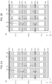
- FIG. 1A illustrates a layout of a cell block formed of a plurality of cells for a two-dimensional (2D) semiconductor device, according to one or more embodiments
- FIG. 1B illustrates a layout of a variant of the cell block of FIG. 1A , according to one or more embodiments.
- a distance between these two boundaries is a cell height of the cell.
- the upper boundary and the lower boundary of a cell refer to two boundaries of the cell opposite to each other in the D2 direction, that is, the cell-height direction, and is referred to as a 1 st boundary and a 2 nd boundary, respectively.
- Each of the cells CE11-CE13 may include a 1 st active region RX1 for p-type metal-oxide-semiconductor transistors (PMOSs) or p-type field-effect transistors (PFETs) and a 2 nd active region RX2 for n-type metal-oxide-semiconductor transistors (NMOSs) or n-type field-effect transistors (NFETs).
- the two active regions RX1 and RX2 having a same width W1 in the D2 direction are arranged in two rows in each of the cells CE11-CE13 and extended in a D1 direction horizontally intersecting the D2 direction.
- the D1 direction refers to a cell-length direction or a channel-length direction.
- these source/drain regions, the channel region and the gate structure may form a PMOS along the 1 st active region RX1 or an NMOS along the 2 nd active region RX2.
- Each of the PMOS and NMOS may be a fin field-effect transistor (FinFET), a nanosheet transistor, a different type of field-effect transistor or a planar transistor.
- each of the 1 st boundary and the 2 nd boundary of each of the cells CE11-CE13 may be disposed a 1 st power rail PR1 formed of a metal or metal compound connecting the cell to a positive voltage source VDD or a 2 nd power rail PR2 connecting the cell to a negative voltage source VSS or ground.
- the power rails PR1 and PR2 both are extended in the D1 direction and may overlap the 1 st boundary and the 2 nd boundary of each cell, respectively, in the D2 direction.
- a region 101 on which the active regions RX1 and RX2 of the cells CE11-CE13 are formed will be a substrate, formed of silicon or its equivalent, or a backside isolation structure formed of a dielectric material such as silicon oxide.
- the backside isolation structure may be formed by replacing at least a portion of the substrate when a backside power distribution network (BSPDN) is formed on a back side of the 2D semiconductor device.
- BSPDN backside power distribution network
- the front side of a semiconductor device may refer to an area above a top surface of the substrate or the backside isolation structure where the active regions RX1, RX2 and the gate structures PC are formed
- the back side of a semiconductor device may refer to an area below a top surface of the substrate or the backside isolation structure.
- the 1 st cell CE11 may be formed by flipping the 2 nd cell CE12 in the D2 direction with respect to the 1 st boundary of the 2 nd cell CE12 which is the 2 nd boundary of the 1 st cell CE11, and similarly the 3 rd cell CE13 may be formed by flipping the 2 nd cell CE12 in the D2 direction with respect to the 2 nd boundary of the 2 nd cell CE12 which is the 1 st boundary of the 3 rd cell CE13.
- This cell flipping may be provided at least to shorten a signal routing path between two 1 st active regions RX1 or two 2 nd active regions RX2, thereby reducing contact resistance to improve connection performance and a device area gain.
- electrical characteristics, performance, and a manufacturing process of a semiconductor device based on the cell block 10A may also be affected by a distance between two adjacent active regions respectively included in two adjacent cells in the D2 direction, which is referred to as RXRXV herein.
- the RXRXV in the cell block 10A may be a distance between the 1 st active regions RX1 of the cells CE11 and CE12 in the D2 direction, and a distance between the 2 nd active regions RX2 of the cells CE12 and CE13 in the D2 direction.
- Performance of a semiconductor device may increase when the RXRXV in a cell block for the semiconductor device is increased.
- the RXRXV may be fixed in a cell block such as the cell block 10A for a 2D semiconductor device.
- the distance D 1 is fixed according to a design rule of the cell block 10A for the semiconductor device which is a 2D semiconductor device, and thus, performance increase of the semiconductor device by changing a cell layout may be limited for the cell block 10A.
- FIG. 1B shows a layout of a cell block 10B which has the same or similar cell arrangement and cell components of the cell block 10A of FIG. 1A except that, in the cell block 10B, a width W1' of each of the two active regions RX1 and RX2 in the cells CE11' and CE13' is smaller than the width W1 of each of the two active regions RX1 and RX2 in the cell CE12'.
- This width difference in active region may be implemented to provide at least an area gain to a semiconductor device to be formed based on the cell block 10B, for example, to facilitate formation of other circuit elements in a space between the two active regions having the decreased width W1'.
- a distance between the two 1 st active regions RX1 of the cells CE11' and CE12' and between the two 2 nd active regions RX2 of the cells CE12' and CE13' is fixed to the distance D1 as in the cell block 10A of FIG. 1A .
- performance increase of the semiconductor device to be formed based on the cell block 10B may also be limited as described above for the cell block 10A.
- the RXRXV may be changed in a cell layout from a 3D-stacked semiconductor device as described below.
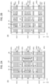
- FIG. 2A illustrates a layout of a cell block formed of a plurality of cells for a three-dimensionally-stacked (3D-stacked) semiconductor device, according to one or more embodiments
- FIG. 2B illustrates a layout of a variant of the cell block of FIG. 2A , according to one or more embodiments.
- a cell block 20A is formed by serially arranging cells CE21-CE23 in the D2 direction in the same manner as the cells CE11-CE13 of FIG. 1A .
- These cells CE21-CE23 may have the same or similar cell arrangement and components of the cell block 10A of FIG. 1A .
- the cells CE21-CE23 of the cell block 20A is provided for a 3D-stacked semiconductor device, and thus, an upper active region RX1 is provided for PMOSs and a lower active region RX2 is provided for NMOSs, respectively, in each of the cells CE21-CE23.
- the upper active region RX1 may partially overlap the lower active region RX2 as will be described later.
- a plurality of gate structures PC extended in the D2 direction cross the two active regions RX1 and RX2 in each of the cells CE21-CE23.
- a portion of each of the two active regions RX1 and RX2 in each of the cells CE21-CE23 which a gate structure PC crosses and surrounds may form a channel region of a transistor structure, and two opposite regions in each of the active regions RX1 and RX2 with respect to the gate structure PC in the D1 direction may form source/drain regions connected to each other through the channel region.
- these source/drain regions, the channel region and the gate structure may form a PMOS along the upper active region RX1 or an NMOS along the lower active region RX2.
- Each of the PMOS and NMOS may be a FinFET, a nanosheet transistor, a different type of field-effect transistor or a planar transistor.
- a region 101 will be a substrate, formed of silicon or its equivalent or a backside isolation structure formed of a dielectric material such as silicon oxide.
- the upper active region RX1 is formed vertically above the lower active region RX2 in a D3 direction to partially overlap the lower active region RX2, and thus, transistors respectively formed in the two active regions RX1 and RX2 may form a 3D transistor structure. Further, a width W21 of the upper active region RX1 may be smaller than a width W22 of the lower active region RX2 in the D2 direction.
- the upper active region RX1 and the lower active region RX2 may be referred to as an upper active region and a lower active region, respectively, in the D3 direction.
- the D3 direction refers to a channel height direction which vertically intersects the D1 and D2 directions which horizontally intersect each other.
- FIGS. 2C and 2D illustrate channel structures and source/drain regions formed on the two active regions RX1 and RX2 may take forms shown in FIGS. 2C and 2D.
- FIG. 2C illustrates an upper channel structure CH1 formed on the upper active region RX1 for an upper nanosheet transistor and a lower channel structure CH2 formed on the lower active region RX2 for a lower nanosheet transistor in a cross-section view taken along a line I-I' shown in FIG. 2A .
- FIG. 2C illustrates an upper channel structure CH1 formed on the upper active region RX1 for an upper nanosheet transistor and a lower channel structure CH2 formed on the lower active region RX2 for a lower nanosheet transistor in a cross-section view taken along a line I-I' shown in FIG. 2A .
- FIG. 2D illustrates an upper source/drain region SD1 formed on the upper active region RX1 for the upper nanosheet transistor and a lower source/drain region SD2 formed on the lower active region RX2 for the lower nanosheet transistor in a cross-section view taken along a line II-II' shown in FIG. 2A .
- the upper channel structure CH1 may include a plurality of nanosheet layers having the width W21 which is smaller than the width W22 of a plurality of nanosheet layers forming the lower channel structure CH2. Accordingly, the upper source/drain region SD1 that may be epitaxially grown from the upper channel structure CH1 may have a smaller width than the lower source/drain region SD2 that may be epitaxially grown from the lower channel structure CH2.
- a region A may be provided along the lower active region RX2 above the lower channel structure CH2 and the lower source/drain region SD2 where the lower active region RX2 including the lower channel structure CH2 and the lower source/drain region SD2 is not overlapped by the upper active region RX1 including the upper channel structure CH1 and the upper source/drain region SD1 in the D3 direction. Due to this region A, which is a non-overlapped region, a contact structure connecting the lower source/drain region SD2 to the voltage source VDD or VSS through the power rails PR1 and PR2 may be formed on a top surface of the lower source/drain region SD2 exposed through the region A.
- the channel structures CH1 and CH2 may be surrounded by a gate structure PC and divided by a middle dielectric layer MDI.
- the source/drain regions SD1 and SD2 may be isolated from each other by an isolation structure ILD.
- the 3 rd cell CE23 may take a form of a flipped cell which is formed by flipping the 2 nd cell CE22 in the D2 direction based on the 2 nd boundary of the 2 nd cell CE22 which is the 1 st boundary of the 3 rd cell CE23.
- the cell flipping in the cell layout of FIG. 2A may be provided at least to shorten a signal routing path between two upper active regions RX1 or two lower active regions RX2, thereby reducing contact resistance to improve connection performance and a device area gain.
- the 3 rd cell CE23 may be oriented with respect to the 2 nd cell CD22 such that the region A above the lower active region RX2 not overlapped by the upper active region RX1 in the 2 nd cell CE22 may face a region B above the lower active region RX2 not overlapped by the upper active region RX1 in the 3 rd cell CE23, as shown in FIG. 2A .
- the 1 st cell CE21 take the same form as the 2 nd cell CD22.
- the cell block 20A may be powered through a plurality of backside power rails BPR1 and BPR2. Placement of backside power rails may not be bound by a cell design rule which strictly requires frontside power rails to be formed on a 1 st boundary and a 2 nd boundary of a cell.
- a 1 st backside power rail BPR1 extended in the D1 direction may be formed to overlap each of a 1 st boundary and a 2 nd boundary of each cell in the cell block 20A
- a 2 nd backside power rail BPR2 extended in the D1 direction may be formed to overlap an inside of each cell, for example, a virtual center line extended in the D1 direction in each cell.
- the 1 st backside power rail BPR1 may connect each cell to a positive voltage source VDD, and the 2 nd backside power rail BPR2 may connect the cell to a negative voltage source VSS or ground.
- These backside power rails BPR1 and BPR2 are included in a BSPDN structure of the 3D-stacked semiconductor device to be formed based on the cell block 20A.
- the BSPDN structure may be formed on a back side of the 3D-stacked semiconductor device, for example, inside a substrate or a backside isolation structure replacing the substrate in the 3D-stacked semiconductor device.
- the 3D-stacked semiconductor device to be formed based on the cell block 20A may also be affected in its electrical characteristics, performance, and a manufacturing process thereof by a distance between two adjacent active regions respectively included in two adjacent cells, that is, RXRXV
- the RXRXV in the cell layout of the cell block 20A may be increased when the cell flipping is performed as shown in FIG. 2A .
- a distance D22 between the upper active region RX1 in the cell CE22 and the upper active region RX1 of the flipped cell CE23 may be greater than a distance D21 between the upper active region RX1 in the cell CE22 and the upper active region RX1 of the non-flipped cell CE21. Still, however, a distance D23 between the lower active regions RX2 of two adjacent cells among the cells CE21-CE23 may be fixed without being changed by the cell flipping.
- the RXRXV may be further extended to additionally improve the electrical characteristics, performance, and manufacturing process of the 3D-stacked semiconductor device to be formed based on the cell block 20A.
- FIG. 2B shows a layout of a cell block 20B which has the same cell arrangement and cell components of the cell block 20A of FIG. 2A except that a width W21' of upper active regions RX1 and a width W22' of the lower active regions RX2 in a cell CE21' and a flipped cell CE23' are smaller than the width W21 of the upper active region RX1 and the width W22 of the lower active region RX2 in the cell CE22, respectively.
- This width difference in active region in the D2 direction may also be implemented to provide at least an area gain to a 3D-stacked semiconductor device to be formed based on the cell block 20B, for example, to facilitate formation of other circuit elements in a space between the active regions of the cell block 20B in the D2 direction.
- the RXRXV may be further increased compared to the RXRXV in the cell block 20A.
- a distance D22' between an upper active region RX1' in the cell CE22' and the upper active region RX1' of the flipped cell CE23' in the cell block 20B may be greater than the distance D22 between the upper active region RX1 in the cell CE22 and the upper active region RX1 in the flipped cell CE23 in the cell block 20A by the width difference (W21'-W21).
- a distance D21' between the upper active region RX1' in the cell CE22' and the upper active region RX1' of the cell CE21' in the cell block 20B may be greater than the distance D21 between the upper active region RX1 in the cell CE22 and the upper active region RX1 in the non-flipped cell CE21 in the cell block 20A by the width difference (W21'-W21).
- a distance D23' between lower active regions RX2' of two adjacent cells among the cells CE21'-CE23' of the cell block 20B may also be greater than the distance D23 between the lower active regions RX2 of two adjacent cells among the cells CE21-CE23 of the cell block 20B by the width difference (W22'-W22).
- the RXRXV may be further increased by adding one or more cell spacers according to one or more embodiments provided herebelow.
- FIGS. 3A illustrates a layout of a cell block formed of a plurality of cells and cell spacers for a 3D-stacked semiconductor device, according to one or more embodiments
- FIG. 3B illustrates a layout of a variant of the cell block of FIG. 3A , according to one or more embodiments.
- a cell block 30A is formed of a plurality of cells CE31-CE33 which have the same cell components as the cells CE21-CE23 of the cell block 20A of FIG. 2A .
- duplicate descriptions thereof are omitted herein, and instead, different aspects of the cell block 30A are described herebelow.
- the cell block 30A differs from the cell block 20A by two cell spacers FC1 and FC2 which are respectively formed between the cells CE31 and CE32 and between the cells CE32 and CE33.
- the cell spacers FC1 and FC2 may each have a cell height H which is a distance between a 1 st boundary and a 2 nd boundary thereof in the D2 direction.
- Power rails BPR1 may be formed to overlap the 1 st and 2 nd boundaries of each of the cell spacers FC1 and FC2.
- the power rails BPR1 may be backside power rails of a BSPDN structure, not being limited thereto.
- the cell spacer FC1 and the cell CE31 may abut each other to share a boundary BR such that the 1 st boundary of the cell spacer FC1 is or overlaps a 2 nd boundary of the cell CE31.
- the cell spacer FC 1 may also abut the cell CE32 to share a boundary BR such that the 2 nd boundary of the cell spacer FC1 is or overlaps a 1 st boundary of the cell CE32.
- the cell spacer FC2 may abut each of the cells CE32 and CE33 in the D2 direction to share their boundaries BR.
- Each of the cell spacers FC1 and FC2 may not be a void space but a physical cell which does not include active regions such as the upper active region RX1 or the lower active region RX2.
- the gate structure PC may still cross the cell spacers FC1 and FC2 and extended in the D2 direction.
- the gate structures PC formed on each of the cells CE31-CE33 may be extended in the D2 direction to cross the cell spacers FC1 and FC2 as shown in FIG. 3A .
- RXRXV in the cell block 30A may be extended to be greater than the RXRXV in the cell block 20A, thereby to additionally improve electrical characteristics, performance, and a manufacturing process of a 3D-stacked semiconductor device to be formed based on the cell block 30A.
- a distance D31 between an upper active region RX1 in a cell CE32 and an upper active region RX1 of a non-flipped cell CE31 in the cell block 30A may be greater than the distance D21 between the upper active region RX1 in the cell CE22 and the upper active region RX1 of the non-flipped cell CE21 in the cell block 20A by the cell height H of the cell spacer FC1.
- a distance D32 between the upper active region RX1 in the cell CE32 and an upper active region RX1 of a flipped cell CE33 in the cell block 30A may be greater than the distance D22 between the upper active region RX1 in the cell CE22 and the upper active region RX1 of the flipped cell CE23 in the cell block 20A by the cell height H of the cell spacer FC2.
- a distance D33 between the lower active regions RX2 of two adjacent cells among the cells CE31-CE33 in the cell block 30A may also be greater than the distance D23 in the cell block 20A by the cell height H of the cell spacer FC1 or FC2.
- the RXRXV in the cell block 30A may be additionally extended as shown in FIG. 3B by reducing widths of active regions in selective cells of the cell block 30A.
- the cell block 30B is formed of a plurality of cells CE31'-CE33' which have the same cell components as the cells CE21'-CE23' of the cell block 20B of FIG. 2B .
- duplicate descriptions thereof are omitted herein, and instead, different aspects of the cell block 30B are described herebelow.
- a width W21' of upper active regions RX1' and a width W22' of lower active regions RX2' in the cell CE31' and the flipped cell CE33' are smaller than the width W21 of the upper active region RX1 and the width W22 of the lower active region RX2 in the cell CE32 of the cell block 30A, respectively.
- this width difference in active region in the D2 direction may also be implemented to provide at least an area gain to a 3D-stacked semiconductor device to be formed based on the cell block 30B, for example, to facilitate formation of other circuit elements in a space between the active regions of the cell block 30B in the D2 direction.
- the RXRXV may be further increased compared to the RXRXV in the cell block 30A.
- a distance D32' between an upper active region RX1' in a cell CE32' and the upper active region RX1' of the flipped cell CE33' in the cell block 30B may be greater than the distance D32 between the upper active region RX1 in the cell CE32 and the upper active region RX1 in the flipped cell CE33 in the cell block 30Aby the width difference (W21'-W21).
- a distance D31' between the upper active region RX1' in the cell CE32' and the upper active region RX1' of the non-flipped cell CE31' in the cell block 30B may be greater than the distance D31 between the upper active region RX1 in the cell CE32 and the upper active region RX1 in the non-flipped cell CE31 in the cell block 20A by the width difference (W21'-W21).
- a distance D33' between lower active regions RX2' of two adjacent cells among the cells CE31'-CE33' of the cell block 30B may also be greater than the distance D33 between the lower active regions RX2 of two adjacent cells among the cells CE31-CE33 of the cell block 30B by the width difference (W22'-W22).
- the cell block 30B may also be obtained by adding the cell spacer FC1 and FC2 in the cell block 20B of FIG. 2B .
- the cell block 20B may take the same layout as the cell block 30B.
- the distance D31' between the upper active region RX1' in a cell CE32' and the upper active region RX1' of the non-flipped cell CE31' in the cell block 30B may be greater than the distance D21' between the upper active region RX1' in the cell CE22' and the upper active region RX1' of the non-flipped cell CE21' in the cell block 20B by a cell height H of the cell spacer FC1.
- the distance D32' between the upper active region RX1' in the cell CE32' and the upper active region RX1' of the flipped cell CE33' in the cell block 30B may be greater than the distance D22' between the upper active region RX1' in the cell CE22' and the upper active region RX1' of the flipped cell CE23' in the cell block 20B by the cell height H of the cell spacer FC2.
- the distance D33' between the lower active regions RX2' of two adjacent cells among the cells CE31'-CE33' in the cell block 30B may also be greater than the distance D23' in the cell block 20B by the cell height H of the cell spacer FC1 or FC2.
- the RXRXV in the cell block 30B may be greater than the RXRXV in the cell blocks 20B and 30A to further improve electrical characteristics, performance, and a manufacturing process of a 3D-stacked semiconductor devices formed based on the cell block 30B.
- each of the cell blocks 30A and 30B may include both the cell spacer FC1 and the cell spacer FC2.
- one of the two cell spacers FC1 and FC2 may not be formed according to one or more other embodiments.
- the cell spacer FC2 may not be formed between the cells CE32 and CE33 and between the cells CE32' and CE33' considering that the RXRXV thereof is sufficiently large, and thus, formation of the cell spacer FC2 may be determined to only increase the size of the cell blocks 30A and 30B.
- the cell spacers FC1 and FC2 are added between two adjacent cells in which the width of the upper active region RX1 or RX1' is smaller than the width of the lower active region RX2 or RX2', respectively, in the D2 direction.
- the disclosure is not limited thereto, and the cell spacers FC1 and FC2 may also be added between the two adjacent cells even when the upper active region RX1 or RX1' and the lower active region RX2 or RX2' have the same width in the D2 direction to increase the RXRXV, according to one or more embodiments.
- at least one of the cells CE31' and CE32' may have two active regions RX1 and RX2 having the same width in the D2 direction.
- the RXRXV is described as between two adjacent active regions of respective two PMOSs at a same level or stack (e.g., upper active regions RX1 or RX1' of upper transistors) of the 3D-stacked semiconductor device.
- the disclosure of cell flipping, cell-width reduction, and cell spacer may also apply to RXRXV between two adjacent active regions of respective two NMOSs (e.g., lower active regions RX2 or RX2' of lower transistors).
- the disclosure may also apply to RXRXV between two adjacent active regions of respective different-polarity two transistors. For example, it is understood from FIGS.
- RXRXV between two adjacent active regions of the same-polarity transistors at a same level or stack e.g., PMOSs or NMOSs
- a distance between two adjacent active regions of different polarity-transistors at different levels or stacks e.g., RXRXV between an RX1 and an RX2 also increases.
- the cell block is formed of only three cells serially arranged in the D2 direction.
- this number of the cells is only an example, and thus, one or more cells, whether they are flipped cells of one of the three cells or not, may be added to the cell block in the D2 direction, according to one or more embodiments.
- the upper active region RX1 or RX1' and the lower active region RX2 or RX2' are provided to form PMOSs and NMOSs, respectively.
- the disclosure is not limited thereto, and each of the two active regions RX1 or RX1' and RX2 or RX2' may be provided to form PMOSs or NMOSs, according to one or more other embodiments.
- the upper active region RX1 or RX1' may be provided to form NMOSs while the lower active region RX2 or RX2' is provided to form PMOSs.
- the 1 st power rail PR1 and the 1 st backside power rail BPR1 are each connected to the positive voltage source VDD, and the 2 nd power rail PR2 and the 2 nd backside power rail BPR2 are each connected to the negative voltage source VSS or ground.
- the disclosure is not limited thereto.
- the 1 st power rail PR1 and the 1 st backside power rail BPR1 may each be connected to the negative voltage source VSS or ground
- the 2 nd power rail PR2 and the 2 nd backside power rail BPR2 may each be connected to the positive voltage source VDD.
- the power rails PR1 and PR2 which are frontside power rails, may be formed on the 1 st and 2 nd boundaries of the cells in the cell blocks 20A, 20B, 30A and 30B.
- FIG. 4 is a schematic block diagram illustrating an electronic device including at least one 3D-stacked semiconductor device formed based on at least one of the cell blocks 20A, 20B, 30A and 30B shown in FIGS. 2A, 2B , 3A and 3B , according to embodiments.
- an electronic device 1000 may include at least one processor 1100, a communication module 1200, an input/output module 1300, a storage 1400, and a buffer random access memory (RAM) module 1500.
- the electronic device 1000 may be a mobile device such as a smartphone or a tablet computer, not being limited thereto, according to embodiments.
- the processor 1100 may include a central processing unit (CPU), a graphic processing unit (GPU) and/or any other processors that control operations of the electronic device 1000.
- the communication module 1200 may be implemented to perform wireless or wire communications with an external device.
- the input/output module 1300 may include at least one of a touch sensor, a touch panel a key board, a mouse, a proximate sensor, a microphone, etc. to receive an input, and at least one of a display, a speaker, etc. to generate an output signal processed by the processor 1100.
- the storage 1400 may be implemented to store user data input through the input/output module 1300, the output signal, etc.
- the storage 1400 may be an embedded multimedia card (eMMC), a solid state drive (SSD), a universal flash storage (UFS) device, etc.
- eMMC embedded multimedia card
- SSD solid state drive
- UFS universal flash storage
- the buffer RAM module 1500 may temporarily store data used for processing operations of the electronic device 1000.
- the buffer RAM 1500 may include a volatile memory such as double data rate (DDR) synchronous dynamic random access memory (SDRAM), low power double data rate (LPDDR) SDRAM, graphics double data rate (GDDR) SDRAM, Rambus dynamic random access memory (RDRAM), etc.
- DDR double data rate
- SDRAM synchronous dynamic random access memory
- LPDDR low power double data rate SDRAM
- graphics double data rate SDRAM graphics double data rate SDRAM
- RDRAM Rambus dynamic random access memory
- the electronic device 1000 may further include at least one sensor such as an image sensor.
- At least one component in the electronic device 1000 may be formed based on at least one of the 3D-stacked semiconductor device formed based on at least one of the cell blocks 20A, 20B, 30A and 30B shown in FIGS. 2A, 2B , 3A and 3B , according to embodiments.
Landscapes
- Semiconductor Integrated Circuits (AREA)
- Physics & Mathematics (AREA)
- Geometry (AREA)
- Design And Manufacture Of Integrated Circuits (AREA)
Applications Claiming Priority (2)
| Application Number | Priority Date | Filing Date | Title |
|---|---|---|---|
| US202363601065P | 2023-11-20 | 2023-11-20 | |
| US18/617,033 US20250167110A1 (en) | 2023-11-20 | 2024-03-26 | Cell block for high-performance semiconductor device |
Publications (2)
| Publication Number | Publication Date |
|---|---|
| EP4557913A2 true EP4557913A2 (de) | 2025-05-21 |
| EP4557913A3 EP4557913A3 (de) | 2025-09-10 |
Family
ID=93520871
Family Applications (1)
| Application Number | Title | Priority Date | Filing Date |
|---|---|---|---|
| EP24212310.7A Pending EP4557913A3 (de) | 2023-11-20 | 2024-11-12 | Zellenblock für hochleistungshalbleiteranordnung |
Country Status (5)
| Country | Link |
|---|---|
| US (1) | US20250167110A1 (de) |
| EP (1) | EP4557913A3 (de) |
| KR (1) | KR20250074584A (de) |
| CN (1) | CN120021372A (de) |
| TW (1) | TW202523149A (de) |
Family Cites Families (7)
| Publication number | Priority date | Publication date | Assignee | Title |
|---|---|---|---|---|
| US10586765B2 (en) * | 2017-06-22 | 2020-03-10 | Tokyo Electron Limited | Buried power rails |
| US10833078B2 (en) * | 2017-12-04 | 2020-11-10 | Tokyo Electron Limited | Semiconductor apparatus having stacked gates and method of manufacture thereof |
| US11367722B2 (en) * | 2018-09-21 | 2022-06-21 | Intel Corporation | Stacked nanowire transistor structure with different channel geometries for stress |
| US11393815B2 (en) * | 2019-08-30 | 2022-07-19 | Taiwan Semiconductor Manufacturing Co., Ltd. | Transistors with varying width nanosheet |
| US12170322B2 (en) * | 2021-05-14 | 2024-12-17 | Samsung Electronics Co., Ltd. | Devices including stacked nanosheet transistors |
| US20230290784A1 (en) * | 2022-03-10 | 2023-09-14 | Samsung Electronics Co., Ltd. | Integrated circuit including active pattern having variable width and method of designing the same |
| US20240282855A1 (en) * | 2023-02-21 | 2024-08-22 | Samsung Electronics Co., Ltd. | Semiconductor device including 3d-stacked field-effect transistors having isolation structure between contact plugs |
-
2024
- 2024-03-26 US US18/617,033 patent/US20250167110A1/en active Pending
- 2024-09-24 KR KR1020240129292A patent/KR20250074584A/ko active Pending
- 2024-10-18 TW TW113139630A patent/TW202523149A/zh unknown
- 2024-11-06 CN CN202411574210.1A patent/CN120021372A/zh active Pending
- 2024-11-12 EP EP24212310.7A patent/EP4557913A3/de active Pending
Also Published As
| Publication number | Publication date |
|---|---|
| US20250167110A1 (en) | 2025-05-22 |
| CN120021372A (zh) | 2025-05-20 |
| EP4557913A3 (de) | 2025-09-10 |
| KR20250074584A (ko) | 2025-05-27 |
| TW202523149A (zh) | 2025-06-01 |
Similar Documents
| Publication | Publication Date | Title |
|---|---|---|
| US11404443B2 (en) | Semiconductor device | |
| US9536881B2 (en) | Semiconductor devices having fin shaped channels | |
| US9704864B2 (en) | Semiconductor devices including an isolation layer on a fin and methods of forming semiconductor devices including an isolation layer on a fin | |
| US9754936B2 (en) | Semiconductor device and method of fabricating the same | |
| US10199499B2 (en) | Semiconductor device including active fin | |
| US9659130B2 (en) | Layout design system for generating layout design of semiconductor device | |
| CN104699884A (zh) | 布图设计系统以及使用该系统制造的半导体器件 | |
| KR102002453B1 (ko) | 반도체 장치 및 그 제조 방법 | |
| US9466703B2 (en) | Method for fabricating semiconductor device | |
| US20240313000A1 (en) | Interconnects at back side of semiconductor device for signal routing | |
| US20240145343A1 (en) | Cell architecture with center-line power rails for stacked field-effect transistors | |
| EP4557913A2 (de) | Zellenblock für hochleistungshalbleiteranordnung | |
| US20240304520A1 (en) | Semiconductor cell architecture including backside power rails | |
| US10128254B2 (en) | Semiconductor device | |
| US20250272467A1 (en) | Filler cell for cell layout for semiconductor device | |
| EP4495999A2 (de) | Zellenarchitektur einer halbleitervorrichtung mit auf der basis eines rückseitigen stromverteilungsnetzes verbundenen halbleiterzellen | |
| US20240413160A1 (en) | Cell architecture with improved backside power rail through engineering change order | |
| US20250159986A1 (en) | Cut-mask patterning to remove corner- rounding of active regions of semiconductor device | |
| US20250118676A1 (en) | Semiconductor device including metal lines having different metal pitches | |
| KR20250061599A (ko) | 반도체 소자 |
Legal Events
| Date | Code | Title | Description |
|---|---|---|---|
| PUAI | Public reference made under article 153(3) epc to a published international application that has entered the european phase |
Free format text: ORIGINAL CODE: 0009012 |
|
| STAA | Information on the status of an ep patent application or granted ep patent |
Free format text: STATUS: THE APPLICATION HAS BEEN PUBLISHED |
|
| AK | Designated contracting states |
Kind code of ref document: A2 Designated state(s): AL AT BE BG CH CY CZ DE DK EE ES FI FR GB GR HR HU IE IS IT LI LT LU LV MC ME MK MT NL NO PL PT RO RS SE SI SK SM TR |
|
| PUAL | Search report despatched |
Free format text: ORIGINAL CODE: 0009013 |
|
| AK | Designated contracting states |
Kind code of ref document: A3 Designated state(s): AL AT BE BG CH CY CZ DE DK EE ES FI FR GB GR HR HU IE IS IT LI LT LU LV MC ME MK MT NL NO PL PT RO RS SE SI SK SM TR |
|
| RIC1 | Information provided on ipc code assigned before grant |
Ipc: H10D 88/00 20250101AFI20250804BHEP Ipc: H10D 89/10 20250101ALI20250804BHEP Ipc: H10D 84/01 20250101ALI20250804BHEP Ipc: H10D 84/83 20250101ALI20250804BHEP Ipc: H10D 30/43 20250101ALI20250804BHEP Ipc: H10D 64/27 20250101ALI20250804BHEP Ipc: H10D 84/03 20250101ALI20250804BHEP Ipc: H10D 84/85 20250101ALI20250804BHEP |
|
| STAA | Information on the status of an ep patent application or granted ep patent |
Free format text: STATUS: REQUEST FOR EXAMINATION WAS MADE |
|
| 17P | Request for examination filed |
Effective date: 20250923 |