EP4557504A1 - Pitchreduzierende lötverbindung für hf-übergänge - Google Patents
Pitchreduzierende lötverbindung für hf-übergänge Download PDFInfo
- Publication number
- EP4557504A1 EP4557504A1 EP24214049.9A EP24214049A EP4557504A1 EP 4557504 A1 EP4557504 A1 EP 4557504A1 EP 24214049 A EP24214049 A EP 24214049A EP 4557504 A1 EP4557504 A1 EP 4557504A1
- Authority
- EP
- European Patent Office
- Prior art keywords
- pair
- electrical interconnect
- interconnect pads
- integrated circuit
- interposer
- Prior art date
- Legal status (The legal status is an assumption and is not a legal conclusion. Google has not performed a legal analysis and makes no representation as to the accuracy of the status listed.)
- Pending
Links
Images


Classifications
-
- H—ELECTRICITY
- H10—SEMICONDUCTOR DEVICES; ELECTRIC SOLID-STATE DEVICES NOT OTHERWISE PROVIDED FOR
- H10W—GENERIC PACKAGES, INTERCONNECTIONS, CONNECTORS OR OTHER CONSTRUCTIONAL DETAILS OF DEVICES COVERED BY CLASS H10
- H10W44/00—Electrical arrangements for controlling or matching impedance
- H10W44/20—Electrical arrangements for controlling or matching impedance at high-frequency [HF] or radio frequency [RF]
-
- H—ELECTRICITY
- H01—ELECTRIC ELEMENTS
- H01Q—ANTENNAS, i.e. RADIO AERIALS
- H01Q1/00—Details of, or arrangements associated with, antennas
- H01Q1/12—Supports; Mounting means
- H01Q1/22—Supports; Mounting means by structural association with other equipment or articles
- H01Q1/2283—Supports; Mounting means by structural association with other equipment or articles mounted in or on the surface of a semiconductor substrate as a chip-type antenna or integrated with other components into an IC package
-
- H—ELECTRICITY
- H01—ELECTRIC ELEMENTS
- H01P—WAVEGUIDES; RESONATORS, LINES, OR OTHER DEVICES OF THE WAVEGUIDE TYPE
- H01P5/00—Coupling devices of the waveguide type
- H01P5/02—Coupling devices of the waveguide type with invariable factor of coupling
- H01P5/022—Transitions between lines of the same kind and shape, but with different dimensions
- H01P5/028—Transitions between lines of the same kind and shape, but with different dimensions between strip lines
-
- H—ELECTRICITY
- H10—SEMICONDUCTOR DEVICES; ELECTRIC SOLID-STATE DEVICES NOT OTHERWISE PROVIDED FOR
- H10W—GENERIC PACKAGES, INTERCONNECTIONS, CONNECTORS OR OTHER CONSTRUCTIONAL DETAILS OF DEVICES COVERED BY CLASS H10
- H10W70/00—Package substrates; Interposers; Redistribution layers [RDL]
- H10W70/01—Manufacture or treatment
- H10W70/05—Manufacture or treatment of insulating or insulated package substrates, or of interposers, or of redistribution layers
-
- H—ELECTRICITY
- H10—SEMICONDUCTOR DEVICES; ELECTRIC SOLID-STATE DEVICES NOT OTHERWISE PROVIDED FOR
- H10W—GENERIC PACKAGES, INTERCONNECTIONS, CONNECTORS OR OTHER CONSTRUCTIONAL DETAILS OF DEVICES COVERED BY CLASS H10
- H10W70/00—Package substrates; Interposers; Redistribution layers [RDL]
- H10W70/60—Insulating or insulated package substrates; Interposers; Redistribution layers
- H10W70/67—Insulating or insulated package substrates; Interposers; Redistribution layers characterised by their insulating layers or insulating parts
- H10W70/68—Shapes or dispositions thereof
- H10W70/685—Shapes or dispositions thereof comprising multiple insulating layers
-
- H—ELECTRICITY
- H10—SEMICONDUCTOR DEVICES; ELECTRIC SOLID-STATE DEVICES NOT OTHERWISE PROVIDED FOR
- H10W—GENERIC PACKAGES, INTERCONNECTIONS, CONNECTORS OR OTHER CONSTRUCTIONAL DETAILS OF DEVICES COVERED BY CLASS H10
- H10W74/00—Encapsulations, e.g. protective coatings
- H10W74/01—Manufacture or treatment
- H10W74/016—Manufacture or treatment using moulds
-
- H—ELECTRICITY
- H10—SEMICONDUCTOR DEVICES; ELECTRIC SOLID-STATE DEVICES NOT OTHERWISE PROVIDED FOR
- H10W—GENERIC PACKAGES, INTERCONNECTIONS, CONNECTORS OR OTHER CONSTRUCTIONAL DETAILS OF DEVICES COVERED BY CLASS H10
- H10W74/00—Encapsulations, e.g. protective coatings
- H10W74/10—Encapsulations, e.g. protective coatings characterised by their shape or disposition
- H10W74/111—Encapsulations, e.g. protective coatings characterised by their shape or disposition the semiconductor body being completely enclosed
-
- H—ELECTRICITY
- H10—SEMICONDUCTOR DEVICES; ELECTRIC SOLID-STATE DEVICES NOT OTHERWISE PROVIDED FOR
- H10W—GENERIC PACKAGES, INTERCONNECTIONS, CONNECTORS OR OTHER CONSTRUCTIONAL DETAILS OF DEVICES COVERED BY CLASS H10
- H10W90/00—Package configurations
-
- H—ELECTRICITY
- H01—ELECTRIC ELEMENTS
- H01P—WAVEGUIDES; RESONATORS, LINES, OR OTHER DEVICES OF THE WAVEGUIDE TYPE
- H01P5/00—Coupling devices of the waveguide type
- H01P5/08—Coupling devices of the waveguide type for linking dissimilar lines or devices
- H01P5/10—Coupling devices of the waveguide type for linking dissimilar lines or devices for coupling balanced lines or devices with unbalanced lines or devices
- H01P5/107—Hollow-waveguide/strip-line transitions
-
- H—ELECTRICITY
- H10—SEMICONDUCTOR DEVICES; ELECTRIC SOLID-STATE DEVICES NOT OTHERWISE PROVIDED FOR
- H10W—GENERIC PACKAGES, INTERCONNECTIONS, CONNECTORS OR OTHER CONSTRUCTIONAL DETAILS OF DEVICES COVERED BY CLASS H10
- H10W44/00—Electrical arrangements for controlling or matching impedance
- H10W44/20—Electrical arrangements for controlling or matching impedance at high-frequency [HF] or radio frequency [RF]
- H10W44/203—Electrical connections
- H10W44/216—Waveguides, e.g. strip lines
-
- H—ELECTRICITY
- H10—SEMICONDUCTOR DEVICES; ELECTRIC SOLID-STATE DEVICES NOT OTHERWISE PROVIDED FOR
- H10W—GENERIC PACKAGES, INTERCONNECTIONS, CONNECTORS OR OTHER CONSTRUCTIONAL DETAILS OF DEVICES COVERED BY CLASS H10
- H10W44/00—Electrical arrangements for controlling or matching impedance
- H10W44/20—Electrical arrangements for controlling or matching impedance at high-frequency [HF] or radio frequency [RF]
- H10W44/241—Electrical arrangements for controlling or matching impedance at high-frequency [HF] or radio frequency [RF] for passive devices or passive elements
- H10W44/248—Electrical arrangements for controlling or matching impedance at high-frequency [HF] or radio frequency [RF] for passive devices or passive elements for antennas
-
- H—ELECTRICITY
- H10—SEMICONDUCTOR DEVICES; ELECTRIC SOLID-STATE DEVICES NOT OTHERWISE PROVIDED FOR
- H10W—GENERIC PACKAGES, INTERCONNECTIONS, CONNECTORS OR OTHER CONSTRUCTIONAL DETAILS OF DEVICES COVERED BY CLASS H10
- H10W72/00—Interconnections or connectors in packages
- H10W72/071—Connecting or disconnecting
- H10W72/072—Connecting or disconnecting of bump connectors
- H10W72/07231—Techniques
- H10W72/07236—Soldering or alloying
-
- H—ELECTRICITY
- H10—SEMICONDUCTOR DEVICES; ELECTRIC SOLID-STATE DEVICES NOT OTHERWISE PROVIDED FOR
- H10W—GENERIC PACKAGES, INTERCONNECTIONS, CONNECTORS OR OTHER CONSTRUCTIONAL DETAILS OF DEVICES COVERED BY CLASS H10
- H10W72/00—Interconnections or connectors in packages
- H10W72/90—Bond pads, in general
- H10W72/931—Shapes of bond pads
- H10W72/932—Plan-view shape, i.e. in top view
-
- H—ELECTRICITY
- H10—SEMICONDUCTOR DEVICES; ELECTRIC SOLID-STATE DEVICES NOT OTHERWISE PROVIDED FOR
- H10W—GENERIC PACKAGES, INTERCONNECTIONS, CONNECTORS OR OTHER CONSTRUCTIONAL DETAILS OF DEVICES COVERED BY CLASS H10
- H10W80/00—Direct bonding of chips, wafers or substrates
- H10W80/701—Direct bonding of chips, wafers or substrates characterised by the pads after the direct bonding
- H10W80/732—Direct bonding of chips, wafers or substrates characterised by the pads after the direct bonding having shape changed during the connecting
-
- H—ELECTRICITY
- H10—SEMICONDUCTOR DEVICES; ELECTRIC SOLID-STATE DEVICES NOT OTHERWISE PROVIDED FOR
- H10W—GENERIC PACKAGES, INTERCONNECTIONS, CONNECTORS OR OTHER CONSTRUCTIONAL DETAILS OF DEVICES COVERED BY CLASS H10
- H10W90/00—Package configurations
- H10W90/701—Package configurations characterised by the relative positions of pads or connectors relative to package parts
- H10W90/721—Package configurations characterised by the relative positions of pads or connectors relative to package parts of bump connectors
- H10W90/724—Package configurations characterised by the relative positions of pads or connectors relative to package parts of bump connectors between a chip and a stacked insulating package substrate, interposer or RDL
Definitions
- Embodiments of the subject matter described herein relate to structures and devices for coupling millimeter-wave signals generated by electronic devices to external structures.
- Miniaturized integrated circuits for millimeter-wave communications and other applications are often coupled to external structures (e.g., antennae) to function as intended.
- a launcher configured to couple millimeter-wave radiation is integrated in a device package along with one or more millimeter-wave integrated circuits. In these applications, device package size and cost is typically increased to accommodate the launcher.
- a system in an example embodiment, includes an integrated circuit device having a first pair of electrical interconnect pads with solderable surfaces; and an interposer circuit board having a second pair of electrical interconnect pads with solderable surfaces, and a first pair of conductive paths spaced to create a radio frequency (RF) transmission line.
- the second pair of electrical interconnect pads are configured to provide electrical coupling to the first pair of electrical interconnect pads through solder connections, and the first pair of conductive paths are electrically coupled to the second pair of electrical interconnect pads.
- the first pair of electrical interconnect pads are noncircular and elongated on a common axis and are configured, during a solder reflow process, to cause solder to flow in a direction of the common axis to form an RF transition between the integrated circuit device and the interposer circuit board.
- Additional example embodiments of the system include the first pair of electrical interconnect pads being elongated directly toward each other on the common axis, or being elongated at an angle relative to the common axis, to provide a component of elongation on the common axis.
- the first pair of electrical interconnect pads may be arranged according to a first pitch
- the second pair of electrical interconnect pads may be arranged according to a second pitch
- the first pitch and second pitch may be equal or unequal.
- the integrated circuit device may include a bare integrated circuit die, and the first pair of electrical interconnect pads may be formed on the bare integrated circuit die.
- the integrated circuit device may include a bare integrated circuit die; a polymer layer formed on the bare integrated circuit die, wherein the polymer layer includes a plurality of conductive traces to redistribute electrical connections from the bare integrated circuit die; and a metallization layer formed on the polymer layer, wherein the metallization layer includes the first pair of electrical interconnect pads having solderable surfaces.
- the first pair of electrical interconnect pads may also be noncircular and elongated, where the RF transition between the integrated circuit device and the interposer circuit board is formed between the first pair of electrical interconnect pads and the second pair of electrical interconnect pads.
- the interposer circuit board may include an RF launcher electrically coupled to the RF transmission line on the interposer circuit board.
- a device in another example embodiment, includes a first pair of conductive paths having a first spacing to create a radio frequency (RF) transmission line; and a first pair of electrical interconnect pads having solderable surfaces configured to be electrically coupled to an integrated circuit device using solder connections, wherein the first pair of electrical interconnect pads have a second spacing greater than the first spacing, and wherein the first pair of electrical interconnect pads are electrically coupled to the RF transmission line, the first pair of electrical interconnect pads are noncircular and elongated on a common axis and are configured, during a solder reflow process, to cause solder to flow in a direction of the common axis to form an RF transition between the integrated circuit device and the interposer circuit board.
- RF radio frequency
- the interposer circuit board include a plurality of noncircular, elongated pairs of electrical interconnect pads, and wherein the first pair of electrical interconnect pads is one of the plurality of noncircular, elongated pairs of electrical interconnect pads, an RF launcher electrically coupled to the RF transmission line, and/or plurality of electrical interconnect pads arranged in a pattern corresponding to an arrangement of contacts of a ball grid array (BGA) package, wherein the plurality of electrical interconnect pads comprise the first pair of electrical interconnect pads.
- the first pair of electrical interconnect pads may be elongated directly toward each other on the common axis, or may be elongated at an angle relative to the common axis, to provide a component of elongation on the common axis.
- a device in another example embodiment, includes a radio frequency (RF) circuit configured to produce RF energy; and a first pair of electrical interconnect pads with solderable surfaces configured to provide electrical coupling to a circuit board using solder connections; wherein the first pair of electrical interconnect pads are electrically coupled to the RF circuit to conduct the RF energy, the first pair of electrical interconnect pads are noncircular and elongated on a common axis and are configured, during a solder reflow process, to cause solder to flow in a direction of the common axis to form an RF transition between the integrated circuit device and the circuit board.
- RF radio frequency
- the integrated circuit device include a bare integrated circuit die, where the first pair of electrical interconnect pads are formed on the bare integrated circuit die.
- the integrated circuit device may include a bare integrated circuit die that includes the RF circuit; a polymer layer formed on the bare integrated circuit die, wherein the polymer layer includes a plurality of conductive traces to redistribute electrical connections from the bare integrated circuit die; and a metallization layer formed on the polymer layer, wherein the metallization layer includes the first pair of electrical interconnect pads with solderable surfaces.
- the integrated circuit device may also include a plurality of noncircular, elongated pairs of electrical interconnect pads, where the first pair of electrical interconnect pads is one of the plurality of noncircular, elongated pairs of electrical interconnect pads. Additionally, the integrated circuit device may include a plurality of electrical interconnect pads arranged in a pattern corresponding to an arrangement of contacts of a ball grid array (BGA) package, wherein the plurality of electrical interconnect pads comprise the first pair of electrical interconnect pads.
- BGA ball grid array
- a method in another example embodiment, includes fabricating an interposer circuit board having a first pair of conductive paths spaced to form a radio frequency (RF) transmission line, and having a first pair of electrical interconnect pads with solderable surfaces being noncircular and elongated on a common axis, wherein the first pair of electrical interconnect pads are electrically coupled to the RF transmission line; and electrically coupling an integrated circuit device to the interposer circuit board, wherein the electrically coupling comprises performing a solder reflow operation to allow solder to flow in a direction of the common axis of the first pair of electrical interconnect pads.
- RF radio frequency
- the method may include the integrated circuit device having a pair of circular or noncircular electrical interconnect pads spaced to be electrically coupled to the first pair of electrical interconnect pads on the interposer circuit board.
- the method may include molding over an integrated circuit die to produce a molded integrated circuit device, wherein the integrated circuit die includes an RF circuit configured to produce RF energy; forming a polymer layer on the molded integrated circuit device, wherein the polymer layer includes a second plurality of conductive paths to redistribute interconnects on the molded integrated circuit device to a ball grid array pattern having a pitch compatible with the interposer circuit board, wherein a second pair of the second plurality of conductive paths are electrically coupled to conduct the RF energy; and forming a metallization layer on the polymer layer to form the integrated circuit device, wherein the metallization layer includes a second pair of electrical interconnect pads electrically coupled to the second pair of the second plurality of conductive paths on the polymer layer to conduct the RF energy, where
- Coupled is defined as directly or indirectly connected in an electrical or non-electrical manner.
- substantially mean sufficient to accomplish the stated purpose in a practical manner and that minor imperfections, if any, are not significant for the stated purpose.
- Miniaturization of radiofrequency and microwave electronics for generating and receiving wireless signals present challenges because of the need for structures such as antennae to couple signals from packaged components (e.g., individual chips, systems on a chip, multichip packages, and the like) to free space. While it can be desirable to integrate such structures directly into a chip package, doing so tends to significantly increase the package size because the minimum dimensions of an antenna are often comparable or significantly larger than the effective wavelength of the signals being transmitted. This can increase production costs and introduce undesirable geometric constraints on component placement within larger systems and devices.
- packaged components e.g., individual chips, systems on a chip, multichip packages, and the like
- millimeter waves having free-space wavelengths between 1-10 mm
- lower frequency regimes i.e., in the MHz range and lower.
- integration of millimeter-wave launchers and other structures can still significantly limit minimum package sizes relative to the size of individual integrated circuits, as illustrated by FIG. 1 .
- FIG. 1 is a cross-sectional view of an example system in one approach.
- the system 100 includes an integrated circuit package (the IC package 105) that contains a radio frequency (RF) circuit (e.g., a millimeter-wave integrated circuit) (the IC 110) which is coupled to a millimeter-wave waveguide transition (a launcher 120) that allows RF signals generated by the IC 110 to be coupled to an external antenna structure 170.
- the IC package 105 may be a ball-grid array (BGA) type package and is shown with solder bumps 107 bonding the IC package 105 to contacts 141 on a substrate 140 (which may be a modified printed circuit board, for example).
- BGA ball-grid array
- the substrate 140 includes a waveguide section 150 that is coupled to the antenna section 170, thereby allowing RF signals generated by the IC 110 to be converted into wireless signals that propagate from the launcher 120 into the waveguide section 150 and finally into the antenna 170 which can radiate the signals into the surrounding environment.
- the walls of the waveguide section 150 are conductive (e.g., metallized) such that the waveguide section operates as a rectangular waveguide defined by electrically conductive walls with a center that can be filled with a dielectric material such as dielectric material of the substrate 140.
- the waveguide section 150 and similar structures described herein may be air-filled, gas-filled, or evacuated cavities within a substrate such as the substrate 140.
- integrating the launcher 120 into the IC package 105 means that the IC package 105 must be larger than both the launcher 120 and the IC 110 individually. Furthermore, integration of the launcher 120 into the IC package 105 introduces constraints on the placement of solder bumps (e.g., the solder bumps 107) or other structures used to couple the IC package 105 to the substrate 140 via the contacts 141. This is because the path between the launcher 120 and the waveguide section 150 cannot be obstructed by conductive material. Placement of the IC package 105 on the substrate 140 is also constrained because the launcher 120 must be positioned directly over the waveguide section 150 to allow radiated energy to be effectively coupled from the launcher 120 into the waveguide section 150.
- solder bumps e.g., the solder bumps 107
- solder bumps 107 may be arranged in order to maintain compatibility with conventional circuit board designs.
- the solder bumps 107 may be spaced with a minimum spacing indicated by the dimension 191 and/or spaced with a regular pitch defined by the dimension 191.
- FIG. 2A shows an example system according to one or more embodiments herein.
- the system 200 includes a package 205 and a substrate 240 (e.g., the substrate 140) with a waveguide section 250 (e.g., the waveguide section 150) coupled to an antenna section 270 (e.g., the antenna section 170).
- the IC package 205 includes an integrated circuit (an IC 210; e.g., the IC 110) and is shown with solder bumps 207 bonding the IC package 205 to an interposer 230 which may be a printed circuit board (PCB) substrate or any other suitable substrate having the features described further below.
- PCB printed circuit board
- the interposer 230 has multiple set of contacts 221, 231 on its top side allowing components such as the IC 210 in the IC package 205 and other components such as the component 212 (represented as a discrete passive device such as an inductor or resistor, as a nonlimiting example) to be physically coupled to the interposer 230.
- the IC package 205 is coupled to the contacts 221, 231 on the top surface of the interposer by solder bumps 207, and the component 212 is depicted as being surface mounted to contacts 221 on the top surface of the interposer via solder reflow, or any other acceptable method, as nonlimiting examples.
- Components such as the IC package 205 and the component 212 may be electrically coupled as needed to contacts (e.g., contacts 241) on the substrate 240 via a second set of contacts 232 on the bottom of the interposer 230 that are in turn coupled to the substrate 240 (e.g., via solder bumps 237, as shown or by any other suitable method).
- the contacts 221, 231 on the top side of the interposer 230 can be connected as needed to the contacts 232 on the bottom side in order to enable electrical connections between components such as the IC package 210 and the component 212 on the top surface of the interposer 230.
- the interposer 230 includes a transition structure (e.g., a launcher 235) which can function similarly to the launcher 120 of FIG. 1 , with one difference being that the launcher 235 is disposed within the interposer 230 rather than within the IC package 205.
- RF signals e.g., millimeter-wave signals
- FIG. 2A RF signals (e.g., millimeter-wave signals) can be coupled from the IC 210 to the launcher 235 via a feed contact 239 coupled to one of the solder ball connections 207.
- the IC 210 within the IC package 205 is shown directly connected to the feed contact 239 via a solder bump connection (one of the solder bumps 207) for purposes of illustration, but that any suitable connection method may be used.
- the IC package 205 may be positioned away from the launcher 235 and coupled to the feed contact 239 via a conductive trace or path on or within the interposer 230. It will be further understood that nothing herein is intended to require the use solder bump connections. Rather, any suitable structures and methods can be used including solder reflow, conductive adhesives, and the like as nonlimiting examples.
- an RF signal generated by the IC 210 is propagated to the interposer 230 through a pair of electrical interconnect pads having solderable surfaces 260 on the IC package 205 through the solder balls 207 to the pair of electrical interconnect pads having solderable surfaces 231 on the interposer 230.
- the pair of electrical contacts 231 couple the RF energy to the launcher 235.
- interposer 230 includes conductive traces or paths coupled to the pair of electrical contacts 231, where the conductive paths are spaced to form an RF transmission line to efficiently propagate the RF energy to the launcher 235.
- the IC package 205 may include conductive traces or paths to propagate the same RF energy from the IC 210 to the pair of electrical contacts 260 on the IC package 205, where the conductive paths are spaced to form an RF transmission line to efficiently propagate the RF energy from the IC 210 to the pair of electrical contacts 260.
- Conductive traces/paths and solderable surfaces may be formed on either or both of the IC 210 and the IC package 205 in any suitable manner. For example, a polymer layer may be formed on the underside of the IC 210.
- the polymer layer may include conductive traces to redistribute the IC interconnect from the surface area occupied by the IC 210 to a larger surface area occupied by the IC package 205.
- a metallization layer may be formed on the polymer layer, and the solderable surfaces of the electrical contact pads 260 may be formed within the metallization layer.
- some embodiments include a launcher disposed on or within the interposer 230.
- a launcher is not included within interposer 230, and the RF energy coupled between the IC package 205 and the interposer 230 is propagated to an RF transition structure other than a launcher.
- RF energy received by the interposer 230 may be propagated using RF transmission lines formed on or within the interposer 230 to a connector suitable to couple the RF energy to an external structure.
- RF energy received by the interposer 230 may be coupled to other interconnect devices formed between the interposer 230 and the substrate 240.
- interposers can have arrangements of contacts that are not typically supported by conventional chip assembly processes, while retaining compatibility with conventional circuit board layouts via compatible contacts on the bottom of the interposer (e.g., the solder bumps 237 of FIG. 2A ).
- the solder bumps 207 may have a spacing defined by the dimension 291 which may be smaller than supported by conventional printed circuit board assembly processes.
- the solder bumps 237 on the opposite side of the interposer 230 may have a spacing defined by the dimension 292 that may maintain compatibility with conventional assembly processes.
- chip packages such as the IC package 205 can be made more compact while still being compatible with conventional printed circuit board layouts and/or conventional design rules when the interposer 230 is bonded to a circuit board or other substrate such as the substrate 240 as pictured.
- the solder bumps 207 or other contacts on interposers such as the interposer 230 may be smaller than conventional solder bumps or other contacts while the solder bump 237 or other contacts on such interposers may be conventionally sized.
- interposers such as the interposer 230
- Another potential advantage of the use of interposers such as the interposer 230 is the ability to place such packages containing millimeter-wave components such as the IC 210 remotely, away from structures such as the launcher 235 or the waveguide section 250, allowing for greater flexibility in the design of larger systems built on printed circuit boards or similar substrates such as the substrate 240.
- FIG. 2B is a top plan view illustration of electrical interconnects between devices represented in FIG. 2A .
- integrated circuit interconnect 250 on the underside of the IC 210 is electrically coupled to the electrical interconnect pads 260 by conductive traces 263.
- Conductive traces 263 have a spacing represented by dimension 261 that forms an RF transmission line at the frequency of interest to efficiently propagate RF signals between the IC 210 and the electrical interconnect pads 260 on the underside of the IC package 205.
- the electric interconnect 250 on the underside of the IC package 205 has a pitch represented by dimension 251 that allows for an efficient transfer of RF energy from the IC 210 to conductive traces 263.
- Conductive traces 263 terminate at electrical interconnect pads 260, which may have a pitch represented by distance 291, also shown in FIG. 2A .
- distance 291 also shown in FIG. 2A .
- the RF transition formed between the IC package 205 and the interposer 230 at electrical interconnect pads 260 may introduce an undesirable level of insertion loss without further embodiments capable of reducing the spacing (e.g., dimension 291).
- the pair of electrical interconnect pads 260 are elongated on a common axis toward each other to reduce an effective distance between the conductive elements that result after solder reflow, to reduce RF insertion loss and to provide a more efficient transfer of RF energy between the IC package 205 and the interposer 230.
- the pair of electrical interconnect pads 231 on the interposer 230 are elongated on a common axis toward each other.
- both the pair of electrical interconnect pads 260 and the pair of electrical interconnect pads 231 are elongated on common axes to reduce an effective distance between the conductive elements at the transition between the IC package 205 and the interposer 230.
- FIGs. 3A and 3B are top plan view illustrations of electrical interconnects between devices represented in FIG. 2A .
- conductive traces 263 form a transmission line between electrical interconnects 250 on IC package 205 and electrical interconnect pads 260.
- electrical interconnect pads 231 shown superimposed on electrical interconnect pads 260
- Conductive traces 310 are formed on the interposer 230 with a spacing suitable form an RF transmission line and to provide an efficient conductive path for RF energy.
- conductive traces 310 may terminate at a launcher, such as launcher 235 ( FIG. 2 ), or may terminate at a different RF transition structure.
- both electrical interconnect pads 260 and electrical interconnect pads 231 are circular, which after a solder reflow operation, provides a distance represented by dimension 312 between conductive elements at the transition between the IC package 205 and the interposer 230.
- dimension 312 is larger than the spacing of either the pair of conductive traces 263 on the IC package 205 or the pair of conductive traces 310 on the interposer 230.
- the increased distance represented by dimension 312 results in insertion loss and reduced efficiency when conducting RF energy across the transition between the IC package 205 and the interposer 230.
- FIG. 3B shows one or more electrical interconnect pads elongated in a manner that reduces the distance between conductors at the transition between the IC package 205 and the interposer 230.
- the pair of electrical interconnect pads 260 located on the IC package 205 and coupled to the pair of conductive traces 263 may be elongated towards each other on a common axis, such as axis 310.
- the pair of electrical interconnect pads 231 located on the interposer 230 and coupled to the pair of conductive traces 310 may be elongated towards each other on a common axis, such as axis 310.
- solder flows to occupy space between the elongated pairs of electrical interconnect pads in the direction of the common axis, thereby reducing the distance (shown by dimension 314) between conductors at the transition between the IC package 205 and the interposer 230.
- the phrase "elongated on a common axis,” refers to any noncircular shape that includes a component in the direction of the common axis.
- some embodiments include a noncircular shape that is elongated directly along the common axis in a direction towards the second pad in the pair.
- some embodiments include a noncircular shape that is elongated at an angle relative to the common axis (e.g., 10, 30, 45 degrees, etc.).
- FIG. 3B shows elongation of both pairs of electrical interconnect pads 260 and 231 towards each other on common axis 310, although not all embodiments are limited in this manner.
- electrical interconnect pads 260 are elongated, and electrical interconnect pads 231 are not elongated.
- electrical interconnect pads 231 are elongated, and electrical interconnect pads 260 are not elongated. Any combination of pairs of elongated pads or pairs of elongated pads and non-elongated pads may be utilized in the various embodiments.
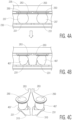
- FIG. 4A is a cross-sectional illustration showing solder balls between an integrated circuit device and interposer circuit board prior to solder reflow.
- the cross section of FIG. 4A shows the IC package 205 and the interposer 230 with solder balls 207 positioned between pairs of electrical interconnect pads.
- the IC package 205 has the pair of conductive traces 263 and the pair of electrical interconnect pads 260 formed on an underside thereof.
- the pair of conductive traces 263 are formed in a polymer layer on the underside of the IC package 205.
- a redistribution layer may be formed using a polymer layer that incorporates conductive traces to redistribute interconnect from an IC within IC package 205.
- the pair of electrical interconnect pads 260 may be formed in a metallization layer that makes electrical contact with traces in the polymer layer.
- the pair of electrical interconnect pads 260 may be formed in an under-bump metallization layer formed on a redistribution layer that is formed on the underside of the IC package 205.
- the interposer 230 has a pair of electrical interconnect pads 231 formed on a surface of the interposer 230 as described above with reference to previous figures.
- the pair of electrical interconnect pads 231 are elongated on a common axis in the plane of the page.
- FIGs. 4B and 4C show solder connections between the IC package 205 and the interposer 230 after a solder reflow operation.
- FIG. 4B is a cross-sectional illustration showing the solder connections
- FIG. 4C is an isometric view illustration showing the solder connections.
- solder from solder balls 207 flows in a direction along the common axis to produce solder connections 407.
- Solder connections 407 flow towards each other on a common axis along solderable surfaces on any pair of elongated electrical interconnect pads. For example, as shown in FIGs.
- the resulting solder connections 407 flow towards each other along the solderable surfaces of the elongated electrical interconnect pads 231, reducing the distance between the electrical conductors near the surface of the interposer 230.
- the pair of electrical interconnect pads 260 on the underside of the IC package 205 are elongated on a common axis, and during solder reflow, the solder flows along the elongated solderable surfaces of the pair of electrical interconnect pads 260 and reduces the distance between the resulting conductors near the surface of the IC package 205.
- both of the pairs of electrical interconnect pads 260 and 231 are elongated on common axes, and the solder flows in a manner that reduces the distance between conductors near both the surface of the IC package 205 and the surface of the interposer 230.
- the conductive traces 263 are eliminated, and solder balls 207 make direct contact with electrical interconnect pads on an integrated circuit die such as the IC 210.
- a polymer layer on the underside of the IC 210 or the IC package 205 may be omitted, and electrical interconnections may be made directly to the IC 210.
- the electrical interconnect pads 260 may be formed directly on the IC to make electrical connections through solder balls 207 to the interposer 230.
- the electrical interconnect pads formed directly on the IC 210 may be elongated on a common axis.
- the electrical interconnect pads on the IC 210 may be circular and the electrical interconnect pads on the interposer 230 may be elongated on the common axis.
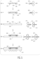
- FIG. 5 shows an example process flow in accordance with various embodiments.
- elongated electrical interconnect pads 260 are formed on an integrated circuit device to provide a solderable surface.
- elongated electrical interconnect pads 260 are formed directly on the IC 210, and in other embodiments, elongated electrical interconnect pads 260 are formed on a surface other than directly on a bare integrated circuit die.
- the IC 210 is molded to form the IC package 205, and a polymer layer may be formed on the underside of the IC package 205 to provide conductive paths such as the pair of conductive pads 263 between integrated circuit interconnects 250 on the underside of the IC package 205 and the electrical interconnect pads 260.
- a metallization layer may be formed on the polymer layer to provide a solderable surface.
- the metallization layer includes the pair of elongated pads 260 that are elongated on a common axis in a direction toward each other.
- more than one pair of elongated electrical interconnect pads may be included on a single IC package.
- a first pair is shown on the underside of the IC package 205 at 260 along with conductive traces 263 and IC interconnects 250, and a second pair of elongated electrical interconnect pads is shown generally at 520. Any number of pairs of elongated electrical interconnect pads may be included on the IC package 205 or the IC 210.
- solder balls are deposited on the pair of elongated electrical interconnect pads 260, and a first solder reflow operation is performed. During the solder reflow operation, the solder wets the solderable surfaces of the pair of elongated electrical interconnect pads 260, resulting in the elongated solder balls shown at 512.
- an interposer circuit board 230 is fabricated.
- the interposer circuit board includes elongated electrical interconnect pads 231 coupled to a pair of conductive paths 310 having a spacing to form an RF transmission line.
- the interposer 230 may include an RF launcher, or other transition mechanism to conduct RF energy off of, or away from, the interposer circuit board 230.
- Solder paste may be applied to the elongated electrical interconnect pads 231 as shown at 531.
- more than one pair of elongated electrical interconnect pads may be included on a single interposer circuit board. For example, a first pair is shown at 231, along with conductive paths 310, and a second pair is shown generally at 522. Any number of pairs of elongated electrical interconnect pads may be included on the interposer circuit board 230.
- the IC package 205 is placed on the interposer circuit board 230 in a manner that superimposes the elongated electrical interconnect pads 260 on the IC package 205 with the elongated electrical interconnect pads 231 on the interposer circuit board as shown at 538.
- a second solder reflow operation is then performed to provide an electrical and mechanical coupling between the electrical interconnect pads 260 on the IC package 205 and the electrical interconnect pads 231 on the interposer circuit board 230.
- the resulting RF transition structure is shown at 540 with solder connections 407 resulting from solder flowing in a direction of the common axis upon which the pairs of electrical interconnect pads have been elongated.
- the IC package 205 is molded over on the interposer circuit board 230, and solder balls 237 are applied to the underside of the interposer circuit board 230.
- the resulting system shown at 510 includes an integrated circuit device coupled to an interposer circuit board where the coupling mechanism includes at least one RF transition structure with reduced insertion loss as a result of one or more pairs of electrical interconnect pads having been elongated on a common axis.
- the integrated circuit device may include a bare integrated circuit die, or may include a bare integrated circuit die along with a package structure that provides a surface for a polymer redistribution layer to redistribute electrical interconnects from the integrated circuit package die to a larger footprint provided by the integrated circuit package and a metallization layer to provide solderable surfaces.
- the integrated circuit board interposer may also include one or more pairs of elongated electrical interconnect pads coupled to one or more pairs of conductive paths having spacing to provide an RF transmission line on or in the interposer circuit board, and may also optionally include a launcher or other RF transition structure.
- FIG. 6 is a flowchart representing example methods in accordance with various embodiments.
- an integrated circuit die that includes a radiofrequency circuit is molded over.
- this corresponds to a bare integrated circuit die (e.g., the IC 210) that includes a millimeter-wave circuit (e.g., an amplifier, transmitter, receiver, etc.) being molded over to produce a molded IC die that has a larger footprint than the bare IC die itself.
- the IC package 205 may result from molding over the IC 210 to provide a molded IC die having a larger footprint suitable for forming interconnect, such as a ball grid array interconnect.
- a polymer layer is formed on the molded IC die. In some embodiments, this may correspond to a redistribution layer being formed on the underside of a molded IC die, such as the IC package 205, to redistribute interconnect from the IC 210 to a different footprint, possibly having a larger pitch.
- a pair of conductive paths are formed in the polymer layer to redistribute IC interconnects and conduct RF energy from the RF circuit included in the IC die.
- a pair of conductive paths 263 may be formed between IC interconnects 250 and the pair of conductive electrical pads 260.
- a metallization layer is formed on the polymer layer that includes at least one pair of elongated electrical interconnect pads having solderable surfaces coupled to the pair of conductive pads.
- an under-bump metallization layer may be formed on the underside of the molded IC die, and the resulting solderable surfaces may include metal contacts that form the electrical interconnect pads 260 that are elongated on a common axis towards each other.
- an interposer circuit board having a pair of conductive paths and a pair of elongated electrical interconnect pads coupled to the pair of conductive paths is fabricated. In some embodiments, this corresponds to fabricating an interposer circuit board using a circuit board substrate and forming the pair of elongated electrical interconnect pads out of circuit board traces where solderable surfaces have been elongated on a common axis toward each other.
- a solder reflow operation is performed to join the molded IC die with the interposer circuit board, where the elongated electrical interconnect pads on the molded IC die are electrically coupled to the elongated electrical interconnect pads on the interposer circuit board.
- the actions of 612 correspond to embodiments in which both the pairs of electrical interconnect pads on an IC package and on an interposer circuit board are elongated on a common axis or on common axes. In some embodiments, a pair of electrical interconnect pads on an IC package are elongated and a corresponding pair of electrical interconnect pads on an interposer circuit board are not elongated.
- a pair of electrical interconnect pads on an IC package are not elongated and a corresponding pair of electrical interconnect pads on an interposer circuit board are elongated.
- a pair of electrical interconnect pads are formed directly on a bare IC die, and that pair of electrical interconnect pads are joined with electrical interconnect pads on an interposer circuit board at 612.
- ICs, IC packages coupled to interposers, and interposers coupled to ICs or IC packages according to embodiments herein can be over molded or otherwise encapsulated to produce a package or interposer with or without an integrated launcher (e.g., as an alternative to the package 105).
- interposers, packages, or ICs can be molded or encapsulated in-place after being coupled to another circuit board or other substrate.
- Such encapsulated structures may also be shielded by enclosing or otherwise surrounding them in suitably conductive material.
- an IC coupled to an interposer is encapsulated in polymeric material.
- such an IC is surrounded by a conductive structure that shields the IC from receiving or generating wireless signal interference.
- FIGs. 7A-7C are cross-sectional illustrations showing example embodiments of systems that include RF transitions.
- Systems 710, 720, and 730 represent example systems that include an integrated circuit device having an RF transition to an interposer circuit board as described herein.
- each of the systems 710, 720, and 730 may include a bare integrated circuit die coupled to an interposer circuit board utilizing at least one pair of elongated electrical interconnect pads, or may include a packaged integrated circuit die coupled to an interposer circuit board utilizing at least one pair of elongated electrical interconnect pads.
- system 710 is coupled to a printed circuit board 712 which includes an antenna or launcher device.
- the interposer circuit board included within system 710 acts as an RF pass-through device that passes the RF signal from the integrated circuit device through the interposer circuit board to the printed circuit board 712 to provide RF energy to the antenna or launcher on the printed circuit board 712.
- system 720 is coupled to a printed circuit board 722 having a waveguide, and the printed circuit board 722 is coupled to an antenna device 724.
- the interposer circuit board included within system 720 may include a launcher that launches the RF energy to the waveguide within the printed circuit board 722.
- system 730 is coupled to a printed circuit board 732.
- the interposer circuit board within system 730 includes an antenna.
- interposer circuit boards that are coupled to integrated circuit devices by low loss RF transitions as described herein may take many forms, and may include or exclude different RF elements such as antennas, launchers, waveguides, and the like.
Landscapes
- Engineering & Computer Science (AREA)
- Microelectronics & Electronic Packaging (AREA)
- Structures For Mounting Electric Components On Printed Circuit Boards (AREA)
Applications Claiming Priority (1)
| Application Number | Priority Date | Filing Date | Title |
|---|---|---|---|
| US18/513,861 US20250167142A1 (en) | 2023-11-20 | 2023-11-20 | Pitch-reducing solder interconnect for rf transitions |
Publications (1)
| Publication Number | Publication Date |
|---|---|
| EP4557504A1 true EP4557504A1 (de) | 2025-05-21 |
Family
ID=93590787
Family Applications (1)
| Application Number | Title | Priority Date | Filing Date |
|---|---|---|---|
| EP24214049.9A Pending EP4557504A1 (de) | 2023-11-20 | 2024-11-19 | Pitchreduzierende lötverbindung für hf-übergänge |
Country Status (2)
| Country | Link |
|---|---|
| US (1) | US20250167142A1 (de) |
| EP (1) | EP4557504A1 (de) |
Citations (3)
| Publication number | Priority date | Publication date | Assignee | Title |
|---|---|---|---|---|
| US5300815A (en) * | 1992-07-17 | 1994-04-05 | Lsi Logic Corporation | Technique of increasing bond pad density on a semiconductor die |
| US6392292B1 (en) * | 1999-07-08 | 2002-05-21 | Nec Corporation | Multi-level stacked semiconductor bear chips with the same electrode pad patterns |
| WO2023218719A1 (ja) * | 2022-05-11 | 2023-11-16 | 日本メクトロン株式会社 | 接合プリント配線板および接合プリント配線板の製造方法 |
-
2023
- 2023-11-20 US US18/513,861 patent/US20250167142A1/en active Pending
-
2024
- 2024-11-19 EP EP24214049.9A patent/EP4557504A1/de active Pending
Patent Citations (3)
| Publication number | Priority date | Publication date | Assignee | Title |
|---|---|---|---|---|
| US5300815A (en) * | 1992-07-17 | 1994-04-05 | Lsi Logic Corporation | Technique of increasing bond pad density on a semiconductor die |
| US6392292B1 (en) * | 1999-07-08 | 2002-05-21 | Nec Corporation | Multi-level stacked semiconductor bear chips with the same electrode pad patterns |
| WO2023218719A1 (ja) * | 2022-05-11 | 2023-11-16 | 日本メクトロン株式会社 | 接合プリント配線板および接合プリント配線板の製造方法 |
Non-Patent Citations (1)
| Title |
|---|
| AI-CHIE WANG ET AL: "Considerations for package routing for DRAM and NAND Flash memory", 2014 IEEE 16TH ELECTRONICS PACKAGING TECHNOLOGY CONFERENCE (EPTC), IEEE, 3 December 2014 (2014-12-03), pages 774 - 779, XP032730975, DOI: 10.1109/EPTC.2014.7028309 * |
Also Published As
| Publication number | Publication date |
|---|---|
| US20250167142A1 (en) | 2025-05-22 |
Similar Documents
| Publication | Publication Date | Title |
|---|---|---|
| EP2626897B1 (de) | Übertragungsleitungsübergang mit einer vertikalen struktur und einzelchip-paket mit landgitter-arrayverbindung | |
| US20230307390A1 (en) | Coaxial through via with novel high isolation cross coupling method for 3d integrated circuits | |
| US6008534A (en) | Integrated circuit package having signal traces interposed between power and ground conductors in order to form stripline transmission lines | |
| US9196951B2 (en) | Millimeter-wave radio frequency integrated circuit packages with integrated antennas | |
| KR101702717B1 (ko) | 밀리미터파 회로 보드를 위한 시스템 및 방법 | |
| KR100511814B1 (ko) | 혼합 신호 인쇄 배선 보드 상의 단일 조립체를 위한저비용, 대용량의 rf 혼성 패키지 | |
| WO2016145960A1 (en) | Package structures having integrated waveguides for high speed communications between package components | |
| US10305196B2 (en) | Dielectric lens structures for EHF radiation | |
| US20090236701A1 (en) | Chip arrangement and a method of determining an inductivity compensation structure for compensating a bond wire inductivity in a chip arrangement | |
| GB2340313A (en) | Shielding electronic packages | |
| US6194669B1 (en) | Solder ball grid array for connecting multiple millimeter wave assemblies | |
| US9589908B1 (en) | Methods to improve BGA package isolation in radio frequency and millimeter wave products | |
| CN105762138A (zh) | 整合式毫米波芯片封装结构 | |
| US9893428B2 (en) | Direct transition from a waveguide to a buried chip | |
| JP2017163385A (ja) | 電子装置及び電子機器 | |
| EP4557504A1 (de) | Pitchreduzierende lötverbindung für hf-übergänge | |
| JP2012209796A (ja) | 高周波モジュール、プリント配線板、プリント回路板、及びアンテナ装置 | |
| US12451579B2 (en) | Interposers with millimeter-wave transitions | |
| US12451578B2 (en) | Interposers with millimeter-wave coaxial-to-waveguide transistions | |
| EP3965303B1 (de) | Drahtloskommunikationsmodul | |
| EP3771028B1 (de) | Halbleitervorrichtung und verfahren | |
| JP2012182682A (ja) | 高周波装置及び高周波モジュール | |
| CN120048815B (zh) | 芯片封装过渡结构、集成天线模块和通信设备 | |
| CN112599480A (zh) | 芯片封装结构、芯片封装方法及电子设备 | |
| JP7660364B2 (ja) | 無線通信モジュール |
Legal Events
| Date | Code | Title | Description |
|---|---|---|---|
| PUAI | Public reference made under article 153(3) epc to a published international application that has entered the european phase |
Free format text: ORIGINAL CODE: 0009012 |
|
| STAA | Information on the status of an ep patent application or granted ep patent |
Free format text: STATUS: THE APPLICATION HAS BEEN PUBLISHED |
|
| AK | Designated contracting states |
Kind code of ref document: A1 Designated state(s): AL AT BE BG CH CY CZ DE DK EE ES FI FR GB GR HR HU IE IS IT LI LT LU LV MC ME MK MT NL NO PL PT RO RS SE SI SK SM TR |
|
| STAA | Information on the status of an ep patent application or granted ep patent |
Free format text: STATUS: REQUEST FOR EXAMINATION WAS MADE |
|
| 17P | Request for examination filed |
Effective date: 20251121 |