EP4557353A2 - Halbleiterbauelement mit integrierter deckelstruktur und verfahren dafür - Google Patents
Halbleiterbauelement mit integrierter deckelstruktur und verfahren dafür Download PDFInfo
- Publication number
- EP4557353A2 EP4557353A2 EP24213114.2A EP24213114A EP4557353A2 EP 4557353 A2 EP4557353 A2 EP 4557353A2 EP 24213114 A EP24213114 A EP 24213114A EP 4557353 A2 EP4557353 A2 EP 4557353A2
- Authority
- EP
- European Patent Office
- Prior art keywords
- lid structure
- encapsulant
- cavity
- semiconductor die
- semiconductor device
- Prior art date
- Legal status (The legal status is an assumption and is not a legal conclusion. Google has not performed a legal analysis and makes no representation as to the accuracy of the status listed.)
- Pending
Links
Images


Classifications
-
- H10W76/161—
-
- H10W76/12—
-
- H10W40/22—
-
- H10W40/778—
-
- H10W42/121—
-
- H10W42/20—
-
- H10W72/071—
-
- H10W74/01—
-
- H10W76/01—
-
- H10W76/60—
-
- H10W72/073—
-
- H10W72/29—
-
- H10W72/332—
-
- H10W72/877—
-
- H10W90/724—
-
- H10W90/736—
Definitions
- This disclosure relates generally to semiconductor device packaging, and more specifically, to a semiconductor device having an integrated lid structure and method of forming the same.
- a semiconductor device having an integrated lid structure.
- the semiconductor device includes a semiconductor die mounted in a cavity of the lid structure such that sidewalls of the lid substantially surround sidewalls of the semiconductor die.
- a backside of the semiconductor die is affixed to the bottom of the cavity by way of a thermally conductive adhesive.
- the mounted semiconductor die and lid structure are at least partially encapsulated with an encapsulant.
- a first portion of the encapsulant the surrounds an outer perimeter of the lid structure and a second portion of the encapsulant substantially fills a gap region of the cavity between the semiconductor die and sidewalls of the cavity. After encapsulation, top and bottom surfaces of the lid structure are exposed, and an active side of the semiconductor die is exposed.
- a plurality of conductive connectors 616 are affixed to respective the die pads 404.
- the conductive connectors 616 are configured and arranged to provide conductive connections between the semiconductor device 100 and a printed circuit board (PCB), for example.
- a plurality of conductive connectors (e.g., solder balls) are affixed to respective die pads of the semiconductor die.
- the conductive connectors are configured and arranged to provide conductive connections between the semiconductor device and a printed circuit board, for example.
- the semiconductor device may be characterized as a high-performance or high-power flip-chip ball grid array (HFCBGA) type device. By forming the semiconductor device in this manner, the integrated lid structure provides enhanced thermal dissipation, electromagnetic interference (EMI) shielding, and warpage control.
- EMI electromagnetic interference
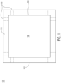
- FIG. 1 illustrates, in a simplified bottom-side-up plan view, an example semiconductor device 100 having an integrated lid structure at a stage of manufacture in accordance with an embodiment.
- the semiconductor device 100 includes a lid structure 102.
- a cavity 104 is formed in the lid structure 102.
- the cavity includes a bottom surface 108 surrounded by sidewalls of the lid structure 102.
- a plurality of grooves e.g., channels
- 106 are formed at the bottom surface 110 of the sidewall portions of the lid structure 102.
- the grooves 106 are configured to allow an encapsulant material (e.g., epoxy mold compound) to flow into and through the cavity 104 as desired during an encapsulation operation at a subsequent stage of manufacture, for example.
- the lid structure is formed from a metal material such as copper, aluminum, and the like.
- the metal material and thickness of the lid structure 102 may be chosen for desired thermal dissipation, electromagnetic interference (EMI) shielding, and warpage control characteristics, for example.
- EMI electromagnetic interference
- the size and shape of the lid structure 102 and corresponding cavity 104 along with the number and locations of the grooves 106 depicted in FIG. 1 are chosen for illustration purposes.
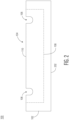
- FIG. 2 illustrates, in a simplified bottom-side-up side view, the example semiconductor device 100 having an integrated lid structure at the stage of manufacture depicted in FIG. 1 in accordance with an embodiment.
- a side portion of the lid structure 102 is illustrated in FIG. 2 .
- the cavity 104 of the lid structure 102 including the bottom surface 108 of the cavity are shown as dashed lines for reference.
- the plurality of grooves 106 are located at the bottom surface 110 of the sidewall portions of the lid structure 102.
- the lid structure 102 is arranged in a bottom side up orientation with the top surface 202 of the lid structure 102 located at the bottom of the illustration.
- FIG. 3 illustrates, in a simplified bottom-side-up plan view, the example semiconductor device 100 having an integrated lid structure at a subsequent stage of manufacture in accordance with an embodiment.
- the semiconductor device 100 includes a thermally conductive adhesive 302 applied on the bottom surface 108 of the cavity 104.
- Thermally conductive adhesive 302 may be applied as a tape or film or otherwise dispensed onto the bottom surface 108 of the cavity 104.
- the thermally conductive adhesive 302 is chosen for consistent, uniform, and accurate bondline thickness (BLT) characteristics when bonding a semiconductor die at a subsequent stage of manufacture, for example.
- BLT bondline thickness
- FIG. 4 illustrates, in a simplified bottom-side-up plan view, the example semiconductor device 100 having an integrated lid structure at a subsequent stage of manufacture in accordance with an embodiment.
- the semiconductor device 100 includes a semiconductor die 402 mounted within the cavity 104 of the lid structure 102.
- the semiconductor die 402 is affixed to the bottom surface 108 of the cavity 104 by way of the thermally conductive adhesive 302 applied on the bottom surface.
- desired consistent, uniform, and accurate BLT can be realized. These desired BLT characteristics may be critical to the reliability of high performance and high power devices, for example.
- the semiconductor die 402 has an active side (e.g., major side having circuitry, die pads) and a backside (e.g., major side opposite of the active side).
- the backside of the semiconductor die 402 is mounted the bottom surface 108 of the cavity 104 while die pads 404 at the active side of the semiconductor die 402 are exposed, for example.
- the semiconductor die 402 is configured in a flip-chip orientation having the die pads 404 at the active side arranged for attachment of conductive connectors (e.g., solder balls) at a subsequent stage of manufacture.
- the active side of the semiconductor die 402 is substantially coplanar with the bottom surface 110 of the sidewall portions of the lid structure 102.
- the semiconductor die 402 may be formed from any suitable semiconductor material, such as silicon, germanium, gallium arsenide, gallium nitride, and the like.
- the semiconductor die 402 may further include any digital circuits, analog circuits, RF circuits, power circuits, memory, processor, MEMs, sensor, the like, and combinations thereof at the active side.
- FIG. 5 illustrates, in a simplified bottom-side-up plan view, the example semiconductor device 100 having an integrated lid structure at a subsequent stage of manufacture in accordance with an embodiment.
- the semiconductor device 100 includes the semiconductor die 402 and the lid structure 102 at least partially encapsulated with an encapsulant 502 (e.g., epoxy molding compound).
- an encapsulant 502 e.g., epoxy molding compound
- the semiconductor die 402 and the lid structure 102 are molded with the encapsulant 502 by way of a molding process.
- the encapsulant 502 may be an epoxy molding compound dispensed during an injection molding encapsulation operation, for example.
- the semiconductor die 402 and the lid structure 102 may be molded with the encapsulant 502 by way of a film-assisted molding (FAM) process.
- FAM film-assisted molding
- a FAM tool using a conformal film may be engaged with predetermined portions of the semiconductor die 402 and the lid structure 102 during the molding process to keep the predetermined portions exposed and free from encapsulant.
- the encapsulant 502 surrounds an outer perimeter of the lid structure and substantially fills a gap region of the cavity between the semiconductor die 402 and sidewalls of the cavity.
- a portion 504 of the encapsulant fills the grooves 106 of FIG. 4 formed at the bottom surface 110 of the sidewall portions of the lid structure 102.
- the bottom surface 110 of the sidewall portions of the lid structure 102 and the active side of the semiconductor die 402 including the die pads 404 are exposed through the encapsulant 502 after the molding process.
- Cross-sectional views of the example semiconductor device 100 taken along line A-A of FIG. 5 at stages of manufacture are depicted in FIG. 6 and FIG. 7 .
- FIG. 6 illustrates, in a simplified top-side-up cross-sectional view, the example semiconductor device 100 having an integrated lid structure at the stage of manufacture depicted in FIG. 5 in accordance with an embodiment.
- the semiconductor device 100 includes the semiconductor die 402 and the lid structure 102 at least partially encapsulated with the encapsulant 502.
- the encapsulant 502 surrounds an outer sidewall surface 608 of the lid structure and substantially fills a gap region 608 of the cavity between sidewalls 602 of the semiconductor die 402 and inner sidewall surfaces 604 of the cavity 104.
- the bottom surface 110 of the sidewall portions of the lid structure 102 and the active side of the semiconductor die 402 including the die pads 404 are exposed through the encapsulant 502 at the bottom side of the semiconductor device 100 after the molding process.
- the top surface 202 of the lid structure 102 is exposed through the encapsulant 502 at the top side of the semiconductor device 100 after the molding process.
- a plurality of conductive connectors 616 e.g., solder balls
- the conductive connectors 616 are configured and arranged to provide conductive connections between the semiconductor device 100 and a printed circuit board (PCB), for example.
- the conductive connectors 616 may be in the form of any suitable conductive structures such as solder balls, gold studs, copper pillars, and the like, to connect conductive features of the semiconductor device 100 with the PCB.
- the die pads 404 may be subsequent connected to the PCB by way of solder paste attachment or other suitable conductive attachment processes (e.g., ACF, ACP).
- a top surface 610 of the encapsulant 502 surrounding the outer sidewall surface 608 of the lid structure 102 is substantially coplanar with the top surface 202 of the lid structure
- a bottom surface 612 of the encapsulant 502 surrounding the outer sidewall surface 608 of the lid structure 102 is substantially coplanar with the bottom surface 110 of the lid structure.
- the bottom surface 612 of the encapsulant 502 surrounding the outer sidewall surface 608 of the lid structure 102 is substantially coplanar with the bottom surface 614 of the encapsulant 502 filling the gap region 608 of the cavity between sidewalls 602 of the semiconductor die 402 and the inner sidewall surfaces 604 of the cavity 104.
- the active side of the semiconductor die 402 is substantially coplanar with the bottom surface 110 of the lid structure 102.
- FIG. 7 illustrates, in a simplified top-side-up cross-sectional view, the example semiconductor device 100 having an integrated lid structure at subsequent stage of manufacture in accordance with an embodiment.
- the semiconductor device 100 includes the encapsulated semiconductor die 402 and the lid structure 102 mounted on an example printed circuit board (PCB) 706.
- the plurality of conductive connectors 616 are affixed to respective connector pads 704 and configured to provide conductive connections between the die pads 404 and respective connector pads 704 of the PCB 706.
- the bottom surface 110 of the lid structure 102 is affixed to respective connector pads 704 by way of a conductive material 702 such as a solder paste or conductive adhesive material.
- the conductive connectors 616 are formed as ball connectors and arranged in a ball grid array.
- the term "conductive,” as used herein, generally refers to electrical conductivity unless otherwise described.
- a method including mounting a semiconductor die within a cavity of a lid structure, an active side of the semiconductor die substantially coplanar with a bottom surface of the lid structure; and encapsulating with an encapsulant to substantially fill a gap region between sidewalls of the semiconductor die and inner sidewall surfaces of the cavity.
- a top surface of the lid structure and the bottom surface of the lid structure may be exposed after encapsulating with the encapsulant.
- the encapsulating with the encapsulant may further include an outer region of the encapsulant surrounding outer sidewall surfaces of the lid structure.
- a bottom surface of the outer region of the encapsulant may be substantially coplanar with a bottom surface of the encapsulant in the gap region.
- a top surface of the outer region of the encapsulant may be substantially coplanar with a top surface of the lid structure.
- the method may further include dispensing a thermally conductive adhesive on a bottom surface of the cavity of the lid structure before mounting the semiconductor die.
- the mounting the semiconductor die within the cavity may include affixing a backside of the semiconductor die to the bottom surface of the cavity by way of the thermally conductive adhesive.
- the lid structure may be formed from a metal material, a plurality of grooves formed at the bottom surface of the lid structure. The plurality of grooves formed at the bottom surface of the lid structure may be configured to allow encapsulant to flow into the cavity.
- a semiconductor device including a lid structure having a top surface and outer sidewall surfaces; a cavity formed in the lid structure, the cavity having a bottom surface and inner sidewall surfaces; a semiconductor die mounted within the cavity such that the inner sidewall surfaces of the cavity surround the semiconductor die; and an encapsulant substantially filling a gap region between sidewalls of the semiconductor die and the inner sidewall surfaces of the cavity.
- An active side of the semiconductor die may be substantially coplanar with a bottom surface of the lid structure.
- a top surface of the lid structure and the bottom surface of the lid structure may be exposed through the encapsulant.
- the encapsulant may include an outer region encapsulating outer sidewall surfaces of the lid structure.
- a bottom surface of the outer region of the encapsulant may be substantially coplanar with a bottom surface of the encapsulant in the gap region.
- the lid structure may include a plurality of grooves formed at the bottom surface of the lid structure, the plurality of grooves configured to allow encapsulant to flow into the cavity during an encapsulation operation.
- a method including providing a lid structure having a top surface and outer sidewall surfaces, the lid structure including a cavity having a bottom surface and inner sidewall surfaces; mounting a semiconductor die within the cavity such that the inner sidewall surfaces of the cavity surround the semiconductor die; and encapsulating with an encapsulant to substantially fill a gap region between sidewalls of the semiconductor die and the inner sidewalls of the cavity.
- An active side of the semiconductor die may be substantially coplanar with a bottom surface of the lid structure after mounting the semiconductor die.
- a top surface of the lid structure and the bottom surface of the lid structure may be exposed after encapsulating with the encapsulant.
- the encapsulating with the encapsulant may further include an outer region of the encapsulant surrounding outer sidewall surfaces of the lid structure.
- the lid structure may include a plurality of grooves formed at the bottom surface of the lid structure, the plurality of grooves configured to allow encapsulant to flow into the cavity.
- the semiconductor device includes a semiconductor die mounted in a cavity of the lid structure such that sidewalls of the lid substantially surround sidewalls of the semiconductor die.
- a backside of the semiconductor die is affixed to the bottom of the cavity by way of a thermally conductive adhesive.
- the mounted semiconductor die and lid structure are at least partially encapsulated with an encapsulant.
- a first portion of the encapsulant the surrounds an outer perimeter of the lid structure and a second portion of the encapsulant substantially fills a gap region of the cavity between the semiconductor die and sidewalls of the cavity.
- top and bottom surfaces of the lid structure are exposed, and an active side of the semiconductor die is exposed.
- a plurality of conductive connectors 616 are affixed to respective the die pads 404.
- the conductive connectors 616 are configured and arranged to provide conductive connections between the semiconductor device 100 and a printed circuit board (PCB), for example.
- a plurality of conductive connectors (e.g., solder balls) are affixed to respective die pads of the semiconductor die.
- the conductive connectors are configured and arranged to provide conductive connections between the semiconductor device and a printed circuit board, for example.
- the semiconductor device may be characterized as a high-performance or high-power flip-chip ball grid array type device. By forming the semiconductor device in this manner, the integrated lid structure provides enhanced thermal dissipation, electromagnetic interference shielding, and warpage control.
Landscapes
- Engineering & Computer Science (AREA)
- Physics & Mathematics (AREA)
- Computer Hardware Design (AREA)
- Condensed Matter Physics & Semiconductors (AREA)
- General Physics & Mathematics (AREA)
- Microelectronics & Electronic Packaging (AREA)
- Power Engineering (AREA)
- Structures Or Materials For Encapsulating Or Coating Semiconductor Devices Or Solid State Devices (AREA)
- Manufacturing & Machinery (AREA)
- Lead Frames For Integrated Circuits (AREA)
- Health & Medical Sciences (AREA)
- Electromagnetism (AREA)
- Toxicology (AREA)
- Chemical & Material Sciences (AREA)
- Materials Engineering (AREA)
Applications Claiming Priority (1)
| Application Number | Priority Date | Filing Date | Title |
|---|---|---|---|
| US18/509,642 US20250157862A1 (en) | 2023-11-15 | 2023-11-15 | Semiconductor device having integrated lid structure and method therefor |
Publications (2)
| Publication Number | Publication Date |
|---|---|
| EP4557353A2 true EP4557353A2 (de) | 2025-05-21 |
| EP4557353A3 EP4557353A3 (de) | 2025-09-17 |
Family
ID=93562774
Family Applications (1)
| Application Number | Title | Priority Date | Filing Date |
|---|---|---|---|
| EP24213114.2A Pending EP4557353A3 (de) | 2023-11-15 | 2024-11-14 | Halbleiterbauelement mit integrierter deckelstruktur und verfahren dafür |
Country Status (2)
| Country | Link |
|---|---|
| US (1) | US20250157862A1 (de) |
| EP (1) | EP4557353A3 (de) |
Family Cites Families (4)
| Publication number | Priority date | Publication date | Assignee | Title |
|---|---|---|---|---|
| JP3466145B2 (ja) * | 2000-09-29 | 2003-11-10 | 沖電気工業株式会社 | 半導体装置とその製造方法 |
| US7235877B2 (en) * | 2004-09-23 | 2007-06-26 | International Rectifier Corporation | Redistributed solder pads using etched lead frame |
| US20090194856A1 (en) * | 2008-02-06 | 2009-08-06 | Gomez Jocel P | Molded package assembly |
| US20220115301A1 (en) * | 2020-10-13 | 2022-04-14 | Amkor Technology Singapore Holding Pte. Ltd. | Semiconductor devices and methods of manufacturing semiconductor devices |
-
2023
- 2023-11-15 US US18/509,642 patent/US20250157862A1/en active Pending
-
2024
- 2024-11-14 EP EP24213114.2A patent/EP4557353A3/de active Pending
Also Published As
| Publication number | Publication date |
|---|---|
| EP4557353A3 (de) | 2025-09-17 |
| US20250157862A1 (en) | 2025-05-15 |
Similar Documents
| Publication | Publication Date | Title |
|---|---|---|
| US7202561B2 (en) | Semiconductor package with heat dissipating structure and method of manufacturing the same | |
| CN100576524C (zh) | 引线框架、半导体封装及其制造方法 | |
| US7141886B2 (en) | Air pocket resistant semiconductor package | |
| CN107230643B (zh) | 具有用于在囊封体中形成开口的延伸结构的封装装置 | |
| EP4369383A1 (de) | Halbleiterbauelement mit hohlraumträger und verfahren dafür | |
| US8643172B2 (en) | Heat spreader for center gate molding | |
| EP4084059A1 (de) | Halbleiterbauelement-packung, das eine wärmeableitung aufweist, und verfahren dafür | |
| EP4593080A1 (de) | Halbleiterbauelement mit doppeltem downset-rahmen und verfahren dafür | |
| EP4632809A1 (de) | Halbleiterbauelement mit eingebettetem flexiblem substrat und verfahren dafür | |
| EP4557353A2 (de) | Halbleiterbauelement mit integrierter deckelstruktur und verfahren dafür | |
| US6879050B2 (en) | Packaged microelectronic devices and methods for packaging microelectronic devices | |
| US20110059579A1 (en) | Method of forming tape ball grid array package | |
| KR100487135B1 (ko) | 볼그리드어레이패키지 | |
| US20230027248A1 (en) | Semiconductor device packaging extendable lead and method therefor | |
| US12388030B2 (en) | Semiconductor device with stress relief feature and method therefor | |
| US8618653B2 (en) | Integrated circuit package system with wafer scale heat slug | |
| US20250157986A1 (en) | Die in die semiconductor device and method therefor | |
| EP4513533A1 (de) | Halbleiteranordnung mit eingebettetem leiterrahmen und verfahren dafür | |
| EP4525027A1 (de) | Halbleiteranordnung mit verbesserter lötbarkeit und verfahren dafür | |
| EP4614561A1 (de) | Elektronische vorrichtung mit verzugsminderung und verfahren dafür | |
| EP4303918A1 (de) | Halbleiterbauelement mit anschlussleitung-auf-chip-verbindung und verfahren dafür | |
| EP4481808A1 (de) | Doppelleiterrahmen-halbleiteranordnung und verfahren dafür | |
| JP2814006B2 (ja) | 電子部品搭載用基板 | |
| KR20060041009A (ko) | 회로 패턴이 형성된 금속 방열판을 구비하는 반도체 패키지 | |
| KR20060024230A (ko) | Elp 구조의 반도체 칩 패키지 및 그 제조방법 |
Legal Events
| Date | Code | Title | Description |
|---|---|---|---|
| PUAI | Public reference made under article 153(3) epc to a published international application that has entered the european phase |
Free format text: ORIGINAL CODE: 0009012 |
|
| STAA | Information on the status of an ep patent application or granted ep patent |
Free format text: STATUS: THE APPLICATION HAS BEEN PUBLISHED |
|
| AK | Designated contracting states |
Kind code of ref document: A2 Designated state(s): AL AT BE BG CH CY CZ DE DK EE ES FI FR GB GR HR HU IE IS IT LI LT LU LV MC ME MK MT NL NO PL PT RO RS SE SI SK SM TR |
|
| PUAL | Search report despatched |
Free format text: ORIGINAL CODE: 0009013 |
|
| AK | Designated contracting states |
Kind code of ref document: A3 Designated state(s): AL AT BE BG CH CY CZ DE DK EE ES FI FR GB GR HR HU IE IS IT LI LT LU LV MC ME MK MT NL NO PL PT RO RS SE SI SK SM TR |
|
| RIC1 | Information provided on ipc code assigned before grant |
Ipc: H01L 21/56 20060101AFI20250811BHEP Ipc: H01L 23/04 20060101ALI20250811BHEP Ipc: H01L 21/60 20060101ALI20250811BHEP Ipc: H01L 23/552 20060101ALN20250811BHEP |