EP4557330A1 - Multilayered capacitor with increased thickness of internal electrodes at the interface with external electrodes - Google Patents
Multilayered capacitor with increased thickness of internal electrodes at the interface with external electrodes Download PDFInfo
- Publication number
- EP4557330A1 EP4557330A1 EP24182592.6A EP24182592A EP4557330A1 EP 4557330 A1 EP4557330 A1 EP 4557330A1 EP 24182592 A EP24182592 A EP 24182592A EP 4557330 A1 EP4557330 A1 EP 4557330A1
- Authority
- EP
- European Patent Office
- Prior art keywords
- thickness
- along
- multilayered capacitor
- capacity
- external electrode
- Prior art date
- Legal status (The legal status is an assumption and is not a legal conclusion. Google has not performed a legal analysis and makes no representation as to the accuracy of the status listed.)
- Pending
Links
Images



Classifications
-
- H—ELECTRICITY
- H01—ELECTRIC ELEMENTS
- H01G—CAPACITORS; CAPACITORS, RECTIFIERS, DETECTORS, SWITCHING DEVICES, LIGHT-SENSITIVE OR TEMPERATURE-SENSITIVE DEVICES OF THE ELECTROLYTIC TYPE
- H01G4/00—Fixed capacitors; Processes of their manufacture
- H01G4/30—Stacked capacitors
-
- H—ELECTRICITY
- H01—ELECTRIC ELEMENTS
- H01G—CAPACITORS; CAPACITORS, RECTIFIERS, DETECTORS, SWITCHING DEVICES, LIGHT-SENSITIVE OR TEMPERATURE-SENSITIVE DEVICES OF THE ELECTROLYTIC TYPE
- H01G4/00—Fixed capacitors; Processes of their manufacture
- H01G4/002—Details
- H01G4/005—Electrodes
-
- H—ELECTRICITY
- H01—ELECTRIC ELEMENTS
- H01G—CAPACITORS; CAPACITORS, RECTIFIERS, DETECTORS, SWITCHING DEVICES, LIGHT-SENSITIVE OR TEMPERATURE-SENSITIVE DEVICES OF THE ELECTROLYTIC TYPE
- H01G4/00—Fixed capacitors; Processes of their manufacture
- H01G4/002—Details
- H01G4/005—Electrodes
- H01G4/012—Form of non-self-supporting electrodes
-
- H—ELECTRICITY
- H01—ELECTRIC ELEMENTS
- H01G—CAPACITORS; CAPACITORS, RECTIFIERS, DETECTORS, SWITCHING DEVICES, LIGHT-SENSITIVE OR TEMPERATURE-SENSITIVE DEVICES OF THE ELECTROLYTIC TYPE
- H01G4/00—Fixed capacitors; Processes of their manufacture
- H01G4/002—Details
- H01G4/228—Terminals
- H01G4/232—Terminals electrically connecting two or more layers of a stacked or rolled capacitor
-
- H—ELECTRICITY
- H01—ELECTRIC ELEMENTS
- H01G—CAPACITORS; CAPACITORS, RECTIFIERS, DETECTORS, SWITCHING DEVICES, LIGHT-SENSITIVE OR TEMPERATURE-SENSITIVE DEVICES OF THE ELECTROLYTIC TYPE
- H01G4/00—Fixed capacitors; Processes of their manufacture
- H01G4/002—Details
- H01G4/228—Terminals
- H01G4/232—Terminals electrically connecting two or more layers of a stacked or rolled capacitor
- H01G4/2325—Terminals electrically connecting two or more layers of a stacked or rolled capacitor characterised by the material of the terminals
Definitions
- the present disclosure relates to a multilayered capacitor
- a multilayered capacitor is a chip-type condenser that is installed at a printed circuit board of various electronic products such as a video device, a computer, a smartphone, a mobile phone, and the like to charge or discharge electricity.
- the multilayered capacitor may be used as a component of various electronic devices due to advantages of a small size, high capacity, and easy mounting. As the component of the electronic device has recently become smaller, a demand for miniaturization and high capacity of the multilayered capacitor is increasing.
- Embodiments are to provide a multilayered capacitor that may improve reliability, may improve connectivity with an external electrode, and may reduce risks of delamination and a radiating crack.
- a multilayered capacitor includes: a body that includes dielectric layers stacked in a first direction and a plurality of internal electrodes disposed to face each other with one of the dielectric layers interposed therebetween; and an external electrode that is disposed on the body and is connected to the internal electrode.
- Each of the plurality of internal electrodes includes a capacity portion disposed to overlap an internal electrode adjacent thereto and a drawing-out portion including a protruding portion extending from the capacity portion to be connected to the external electrode and protruding from one surface of the body in a second direction perpendicular to the first direction, and a portion having a thickness greater than a thickness of the capacity portion along the first direction, and wherein a ratio of a length of the protruding portion along the second direction to the thickness of the capacity portion is within a range of 0.07 or more and less than 0.1.
- the drawing-out portion may further include a portion having a thickness that is along the first direction and that increases toward the outside of the body along the second direction.
- the thickness that increases toward the outside of the body gradually increases toward the outside of the body along the second direction along the first direction.
- the drawing-out portion may further include a portion having a constant thickness along the first direction.
- the protruding portion may include a portion having a constant thickness.
- the drawing-out portion may further include a portion having a thickness that is along the first direction and that increases in opposing directions along the first direction and toward the outside of the body along the second direction.
- the drawing-out portion may further include a portion having a thickness that is along the first direction and that increases in one direction along the first direction and toward the outside of the body along the second direction.
- a ratio of a maximum thickness, which is along the first direction, of the drawing-out portion to an average thickness of the capacity portion may be within a range of greater than 1.2 and less than 2.0.
- the protruding portion may be covered by the external electrode.
- the body may include a first surface and a second surface facing each other in the first direction, a third surface and a fourth surface facing each other in the second direction, and a fifth surface and a sixth surface facing each other in a third direction perpendicular to the first direction and the second direction
- the external electrode may include a first external electrode and a second external electrode
- the plurality of internal electrodes may include a first internal electrode and a second internal electrode that are alternately disposed with the one of the dielectric layers interposed therebetween
- the first internal electrode may include a first capacity portion and a first drawing-out portion including a first protruding portion extending from the first capacity portion to be connected to the first external electrode and protruding from the third surface of the body
- the second internal electrode may include a second capacity portion that overlaps the first capacity portion in the first direction and a second drawing-out portion including a second protruding portion extending from the second capacity portion to be connected to the second external electrode and protruding from the fourth surface of the body.
- the first protruding portion may be covered by the first external electrode, and the second protruding portion may be covered by the second external electrode.
- the external electrode may include: a conductive layer disposed on a surface of the body and connected to the plurality of internal electrodes; and a plating layer disposed on the conductive layer.
- the protruding portion may have a thickness greater than the thickness of the capacity portion along the first direction.
- the protruding portion may be a thickest portion of each of the plurality of internal electrodes.
- the length of the protruding portion may be in a range of 28 nm to 40 nm.
- reliability may be improved by improving a shape of a chip, connectivity with an external electrode may be improved, delamination may be prevented, and a risk of a radiating crack may be reduced.
- FIG. 7 is a cross-sectional view showing a portion of the multilayered capacitor according to another modified example taken along the line II-II' in FIG. 1 .
- the phrase “on a plane” means viewing a target portion from the top
- the phrase “on a cross-section” means viewing a cross-section formed by perpendicularly cutting a target portion from the side.
- the part when it is described that a part is “coupled” to another part, the part may be “directly or physically connected” to the other part or “indirectly or non-contact coupled” to the other part with a third part therebetween.
- a part when it is described that a part is “connected” to another part, the part may be “directly connected” to the other element, may be “connected” to the other part through a third part, or may be connected to the other part physically or electrically, and may be referred to by different titles depending on positions or functions, but respective portions that are substantially integrated into one body may be connected to each other.
- a direction of a body 110 is defined to clearly describe an embodiment of the present disclosure.
- X, y, and z shown in the drawings indicate a length direction, a width direction, and a thickness direction of the body 110, respectively.
- a z-axis direction (the thickness direction; the first direction) may be a direction perpendicular to a wide surface (a main surface) of a constituent element having a sheet shape.
- the z-axis direction (the thickness direction) may be used as the same concept as a stacking direction in which dielectric layers 111 is stacked.
- An x-axis direction (the length direction; the second direction) may be a direction that extends parallel to the wide surface (the main surface) of the constituent element having the sheet shape, and may be a direction approximately perpendicular to the z-axis direction (the thickness direction).
- the x-axis direction (the length direction) may be a direction in which first and second external electrodes 130 and 140 are disposed at both surfaces.
- a y-axis direction (the width direction; the third direction) may be a direction that extends parallel to the wide surface (the main surface) of the constituent element having the sheet shape, and may be a direction approximately perpendicular to the z-axis direction (the thickness direction) and the x-axis direction (the length direction), and a length of the constituent element having the sheet shape in the x-axis direction (the length direction) may be greater than a width of the constituent element having the sheet shape in the y-axis direction (the width direction).
- a first direction that is a direction in which the dielectric layer 111 and first and second internal electrodes 121 and 122 are stacked may be the z-axis direction (the thickness direction), and second and third directions that are perpendicular to the first direction and are perpendicular to each other may be the x-axis direction (the length direction) and the y-axis direction (the width direction), respectively.
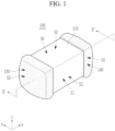
- FIG. 1 is a perspective view schematically showing a multilayered capacitor according to an embodiment of the present disclosure
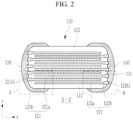
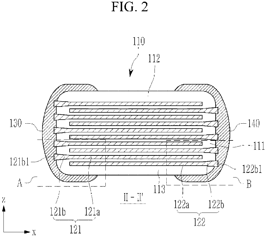
- FIG. 2 is a cross-sectional view taken along a line II-II' in FIG. 1 .
- the multilayered capacitor 100 includes the body 110 and the first and second external electrodes 130 and 140.
- the body 110 may include a plurality of dielectric layers 111, and a plurality of first internal electrodes 121 and a plurality of second internal electrodes 122 alternately disposed in the z-axis direction with the dielectric layer 111 interposed therebetween
- the body 110 may be formed by stacking a plurality of dielectric layers 111 in the z-axis direction and then firing the stacked dielectric layers, and a boundary between adjacent dielectric layers 111 may be integrated to an extent that it is difficult to check without using a scanning electron microscope (SEM).
- SEM scanning electron microscope
- the body 110 may have a thickness along the z-axis direction with a predetermined size, a length along the x-axis direction with a predetermined size, and a width along the y-axis direction with a predetermined size, and may have a substantially hexahedral shape.
- a shape and a dimension of the body 110 and the number of the stacked dielectric layers 111 are not limited to those shown in the drawings of the present disclosure.
- both surfaces of the body 110 facing each other in the z-axis direction are defined as a first surface and a second surface S1 and S2
- both surfaces connected to the first surface and the second surface S1 and S2 and facing each other in the x-axis direction are defined as a third surface and a fourth surface S3 and S4
- both surfaces connected to the first and second surfaces S1 and S2 and the third and fourth surfaces S3 and S4 and facing each other in the y-axis direction are defined as a fifth surface and a sixth surface S5 and S6.
- a mounting surface of the multilayered capacitor 100 may be the first surface S1 of the body 110.
- the dielectric layer 111 may include a ceramic material with a high dielectric constant.
- the dielectric layer 111 may include a barium titanate (BaTiOs)-based ceramic powder or a strontium titanate (SrTiO 3 )-based ceramic powder, but the present disclosure is not limited thereto as long as sufficient capacitance may be obtained.
- a ceramic additive an organic solvent, a plasticizer, a binder, a dispersant, and the like may be further added to the dielectric layer 111 together with the ceramic powder.
- a ceramic additive for example, transition metal oxide, transition metal carbide, a rare earth element, magnesium (Mg), aluminum (Al), or the like may be used as the ceramic additive.
- the body 110 may include an active region that is a portion contributing to form ing capacitance of the capacitor, and upper and lower covers 112 and 113 respectively formed at upper and lower portions of the active region in the z-axis direction that are a vertical margin portion.
- the upper and lower covers 112 and 113 may have the same material and configuration as those of the dielectric layer 111 except that they do not include an internal electrode.
- the upper and lower covers 112 and 113 may be formed by stacking a single dielectric layer or two or more dielectric layers in the z-axis direction on upper and lower surfaces of the active region, respectively. Basically, the upper and lower covers 112 and 113 may serve to prevent damage to the first and second internal electrodes 121 and 122 due to a physical or chemical stress.
- the first and second internal electrodes 121 and 122 may be electrodes receiving different polarities, and may be alternately disposed in the z-axis direction with the dielectric layer 111 interposed therebetween. One ends of the first and second internal electrodes 121 and 122 may be exposed from the third and fourth surfaces S3 and S4 of the body 110, respectively. In addition, the one ends of the first and second internal electrodes 121 and 122 may protrude from the third and fourth surfaces S3 and S4 of the body 110, respectively.
- the first and second internal electrodes 121 and 122 may be electrically insulated from each other by the dielectric layer 111 disposed between the first and second internal electrodes 121 and 122.
- the end portions of the first and second internal electrodes 121 and 122 alternately exposed through the third and fourth surfaces S3 and S4 of the body 110 may be electrically connected to the first and second external electrodes 130 and 140 disposed on the third and fourth surfaces S3 and S4 of the body 110 to be described later, respectively. Therefore, it is possible to improve a bonding strength between the internal electrode and the external electrode, reduce a contact defect, and prevent a decrease in capacity of the multilayered capacitor 100.
- first and second internal electrodes 121 and 122 are not particularly limited.
- the first and second internal electrodes 121 and 122 may be formed using a conductive paste made of one or more materials of a precious metal material such as platinum (Pt), palladium (Pd), a palladium-silver (Pd-Ag) alloy, or the like, nickel (Ni), and copper (Cu).
- a printing method of the conductive paste may be a screen printing method, a gravure printing method, or the like, and the present disclosure is not limited thereto.
- the first internal electrode 121 may include a first capacity portion (or a first capacitance portion) 121a and a first drawing-out portion (or a first drawn-out portion) 121b.
- the first capacity portion 121a may be a portion disposed to be spaced apart from the third to sixth surfaces S3, S4, S5, and S6 of the body 110, and may be a portion that contributes to forming capacitance of the capacitor.
- the first drawing-out portion 121b may be a portion that extends from the first capacity portion 121a to be connected to the first external electrode 130.
- the first drawing-out portion 121b may extend from the first capacity portion 121a to protrude from the third surface S3 of the body 110.
- the first drawing-out portion 121b may include a first protruding portion 121b1 protruding in the x-axis direction from the third surface S3 of the body 110.
- the second internal electrode 122 may include a second capacity portion (or a second capacitance portion) 122a and a second drawing-out portion 122b.
- the second capacity portion 122a may be a portion disposed to be spaced apart from the third to sixth surfaces S3, S4, S5, and S6 of the body 110, and may be a portion that contributes to forming capacitance of the capacitor.
- the second drawing-out portion 122b may extend from the second capacity portion 122a to be connected to the second external electrode 140.
- the second drawing-out portion 122b may extend from the second capacity portion 122a to protrude from the fourth surface S4 of the body 110.
- the second drawing-out portion 122b may include a second protruding portion 122b1 protruding in the x-axis direction from the fourth surface S4 of the body 110.
- the first and second internal electrodes 121 and 122 may include the first and second protruding portions 121b1 and 122b1 that protrude to the outside of the body 110, so that contact with the external electrode may be improved.
- the first and second drawing-out portions 121b and 122b may be disposed to deviate from each other in the length direction of the body 110 to be alternately exposed at both end portions along the length direction of the body 110.
- capacitance of the multilayered capacitor 100 is proportional to overlapped areas of the first capacity portion 121a of the first internal electrode 121 and the second capacity portion 122a of the second internal electrode 122 that overlap each other along the z-axis direction in the active region of the body 110.
- the first and second external electrodes 130 and 140 may be provided with voltages having different polarities, may be disposed at both end portions along the x-axis direction of the body 110, and may be electrically connected to exposed portions of the first and second internal electrodes 121 and 122, respectively.
- the first external electrode 130 may be electrically connected to a plurality of first drawing-out portions 121b
- the second external electrode 140 may be electrically connected to the second drawing-out portion 122b that will be described later.
- the first external electrode 130 may be disposed on a surface of the body 110.
- the first external electrode 130 may include a conductive layer (not shown) connected to the plurality of first internal electrodes 121 and at least one plating layer (not shown) disposed on the conductive layer.
- the plating layer may be disposed to cover the conductive layer.
- the second external electrode 140 may be disposed on the surface of the body 110.
- the second external electrode 140 may include a conductive layer (not shown) connected to the plurality of second internal electrodes 122 and at least one plating layer (not shown) disposed on the conductive layer.
- the plating layer may be disposed to cover the conductive layer.
- the conductive layer may include a connection portion and a band portion.
- the connection portion may be disposed on the third surface S3 or the fourth surface S4 of the body 110, and may be connected to protruded portion of the first internal electrode 121 or the second internal electrode 122.
- the band portion may include a portion extending from the connection portion to a portion of the first surface S1 of the body 110. The band portion may further extend to portions of the fifth and sixth surfaces S5 and S6 and a portion of the second surface S2 of the body 110 to improve an adhesion strength.
- the conductive layer may include at least one of copper (Cu) and silver (Ag), and may further include glass, epoxy, and the like.
- the conductive layer may be formed by applying a conductive paste including a metal and firing the applied conductive paste.
- the plating layer may be formed by including nickel (Ni), phosphorus (P), or palladium (Pd). Additionally, the plating layer may be formed by electroless plating. A plating characteristic of the electroless plating may be not significantly different from that of electrolytic plating, and the plating layer formed by the electroless plating may have better corrosion resistance than a film formed by the electrolytic plating, and may grow substantially equally for each position to have a uniform plating thickness. In addition, because the electroless plating performs plating on only an object to be plated without a dummy, it is easier to prepare for the plating and to sort out a defect of the object to be plated after the plating.
- first and second internal electrodes 121 and 122 will be described in detail with reference to FIG. 2 and FIG. 3 .
- FIG. 3 is an enlarged cross-sectional view of a portion A of FIG. 2
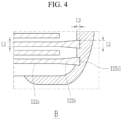
- FIG. 4 is an enlarged cross-sectional view of a portion B of FIG. 2 .
- the first drawing-out portion 121b may be disposed at one end of the first capacity portion 121a.
- the first drawing-out portion 121b may include a portion having a thickness greater than a thickness L1 along the z-axis direction of the first capacity portion 121a.
- a thickness L2 along the z-axis direction of the first drawing-out portion 121b may be greater than the thickness L1 along the z-axis direction of the first capacity portion 121a.
- the second drawing-out portion 122b may be disposed at one end of the second capacity portion 122a.
- the second drawing-out portion 122b may include a portion having a thickness greater than a thickness L1 along the z-axis direction of the second capacity portion 122a.
- a thickness L2 along the z-axis direction of the second drawing-out portion 122b may be greater than the thickness L1 along the z-axis direction of the second capacity portion 122a.
- the thickness L1 of each of the first and second capacity portions 121a and 122a may be a length of an arbitrary line segment connected from one point of a lower surface of each of the first and second capacity portions 121a and 122a to an upper surface thereof or an arithmetic average value of lengths of a plurality of line segments connected from the one point of the lower surface of each of the first and second capacity portions 121a and 122a to the upper surface thereof in an x-z cross-section passing through a central point of the y-axis direction of the multilayered capacitor 100.
- the plurality of line segments described above may be five or more line segments disposed at equal intervals.
- each of the first and second capacity portions 121a and 122a may be measured using an optical microscope, a scanning electron microscope, or the like. Other methods and/or tools appreciated by one of ordinary skill in the art, even if not described in the present disclosure, may also be used.
- the thickness L2 of each of the first and second drawing-out portions 121b and 122b may be a length of an arbitrary line segment connected from one point of a lower surface of each of the first and second drawing-out portions 121b and 122b to an upper surface thereof, a maximum value among lengths of a plurality of line segments connected from the one point of the lower surface of each of the first and second drawing-out portions 121b and 122b to the upper surface thereof, or an arithmetic average value of the lengths of the plurality of line segments in an x-z cross-section passing through a central point of the y-axis direction of the multilayered capacitor 100.
- the plurality of line segments described above may be five or more line segments disposed at equal intervals.
- each of the first and second drawing-out portions 121b and 122b may be measured using an optical microscope, a scanning electron microscope, or the like. Other methods and/or tools appreciated by one of ordinary skill in the art, even if not described in the present disclosure, may also be used.
- the first drawing-out portion 121b may include the first protruding portion 121b1 at one end thereof.
- a ratio of a length L3 along the x-axis direction of the first protruding portion 121b1 to the thickness L1 of the first capacity portion 121a may be in a range of 0.07 or more and less than 0.1.
- the second drawing-out portion 122b may include the second protruding portion 122b1 at one end thereof.
- a ratio of a length L3 along the x-axis direction of the second protruding portion 122b1 to the thickness L1 of the second capacity portion 122a may be in a range of 0.07 or more and less than 0.1.
- the ratio of the length L3 along the x-axis direction of the first protruding portion 121b1 to the thickness L1 of the first capacity portion 121a may be in a range of 0.07 or more and 0.09 or less. Additionally, the ratio of the length L3 along the x-axis direction of the second protruding portion 122b1 to the thickness L1 of the second capacity portion 122a may be in a range of 0.07 or more and 0.09 or less.
- the length L3 of each of the first and second protruding portions 121b1 and 122b1 may be a maximum value, a minimum value, or an arithmetic average value of lengths of a plurality of line segments connected from one end of each of the first and second protruding portions 121b1 and 122b1 to the other end thereof in an x-z cross-section passing through a central point of the y-axis direction of the multilayered capacitor 100.
- the plurality of line segments described above may be five or more line segments disposed at equal intervals.
- the length L3 of each of the first and second protruding portions 121b1 and 122b1 may be measured using an optical microscope, a scanning electron microscope, or the like.
- the ratio of the length L3 of the first protruding portion 121b1 to the thickness L1 of the first capacity portion 121a or the ratio of the length L3 of the second protruding portion 122b1 to the thickness L1 of the second capacity portion 122a is less than 0.07, a radiating crack may be highly likely to occur. If the ratio of the length L3 of the first protruding portion 121b1 to the thickness L1 of the first capacity portion 121a or the ratio of the length L3 of the second protruding portion 122b1 to the thickness L1 of the second capacity portion 122a is 0.1 or more, a falling out of the electrode may occur.
- the ratio of the length L3 of the first protruding portion 121b1 to the thickness L1 of the first capacity portion 121a or the ratio of the length L3 of the second protruding portion 122b1 to the thickness L1 of the second capacity portion 122a is 0.07 or more and less than 0.1, a risk of the radiating crack may be reduced.
- thicknesses of the first and second internal electrodes 121 and 122 may be 360 nm to 440 nm or 400 nm.
- the length L3 along the x-axis direction of each of the first and second protruding portions 121b1 and 122b1 may be within a range of 28 nm to 40 nm.
- the first and second drawing-out portions 121b and 122b may include a portion in which a thickness increases along the z-axis direction.
- the first and second drawing-out portions 121b and 122b may include the portion whose thickness gradually increases toward the outside of the body 110 along the x-axis direction.
- the first and second drawing-out portions 121b and 122b may have a constant ratio of the amount of change in the z-axis direction to the amount of change in the x-axis direction.
- the first and second drawing-out portions 121b and 122b may have a straight line shape with a constant slope.
- the first and second drawing-out portions 121b and 122b may include a portion whose thickness increases in both vertical directions along the z-axis direction toward the outside of the body 110 along the x-axis direction.
- a ratio of a maximum thickness along the z-axis direction of the first drawing-out portion 121b to the thickness L1 along the z-axis direction of the first capacity portion 121a may be in a range of more than 1.2 and less than 2.0. Additionally, a ratio of a maximum thickness along the z-axis direction of the second drawing-out portion 122b to the thickness L1 along the z-axis direction of the second capacity portion 122a may be in a range of more than 1.2 and less than 2.0.
- the ratio of the maximum thickness along the z-axis direction of the first drawing-out portion 121b to the thickness L1 along the z-axis direction of the first capacity portion 121a may be in a range of 1.3 or more and 1.9 or less. Additionally, the ratio of the maximum thickness along the z-axis direction of the second drawing-out portion 122b to the thickness L1 along the z-axis direction of the second capacity portion 122a may be in a range of 1.3 or more and 1.9 or less.
- the ratio of the maximum thickness along the z-axis direction of the first drawing-out portion 121b to the thickness L1 along the z-axis direction of the first capacity portion 121a or the ratio of the maximum thickness along the z-axis direction of the second drawing-out portion 122b to the thickness L1 along the z-axis direction of the second capacity portion 122a is 1.2 or less, an effect of improving high-temperature reliability may be small.
- the ratio of the maximum thickness along the z-axis direction of the first drawing-out portion 121b to the thickness L1 along the z-axis direction of the first capacity portion 121a or the ratio of the maximum thickness along the z-axis direction of the second drawing-out portion 122b to the thickness L1 along the z-axis direction of the second capacity portion 122a is greater than 2.0, a short circuit may occur due to overlapping of vertically adjacent internal electrodes.
- the ratio of the maximum thickness along the z-axis direction of the first drawing-out portion 121b to the thickness L1 along the z-axis direction of the first capacity portion 121a or the ratio of the maximum thickness along the z-axis direction of the second drawing-out portion 122b to the thickness L1 along the z-axis direction of the second capacity portion 122a is within a range greater than 1.2 and less than 2.0, high-temperature reliability may be improved by increasing a thickness of the dielectric layer at both end edges along the x-axis direction of the body where the first and second drawing-out portions 121b and 122b are disposed.
- the first protruding portion 121b1 may be covered by the first external electrode 130.
- the second protruding portion 122b1 may be covered by the second external electrode 140.
- a ratio of a thickness of the drawing-out portion to a thickness of the capacity portion may be 1.6.
- the multilayered capacitor 100 of the embodiment has the breakdown voltage (BDV) increased by about 33% and the high-temperature reliability increased by about 23% or about 52% compared with the comparative example.
- BDV breakdown voltage
- An angle may mean an angle at which the drawing-out portions 121b and 122b are inclined with respect to a line parallel to the x-axis.
- a step difference between adjacent drawing-out portions 121b and 122b of both end edges of the x-axis direction of the body 110 and inclined angles of the drawing-out portions 121b and 122b may be measured by observing a cross-section of the multilayered capacitor using an optical microscope, a scanning electron microscope, or the like.
- Table 3 Comparative Example Embodiment Step difference ( ⁇ m) 25.5 23.8 Angle (degree) 44 33
- the multilayered capacitor 100 of the embodiment has a smaller step difference than that of the comparative example and has a smaller inclined angle than that of the comparative example. Therefore, a problem of deterioration of the BDV and a highly accelerated life test (HALT) due to cumulative stacking at both end edges of the x-axis direction of the body 110 may be improved, and electrode connectivity with the external electrode may be improved.
- HALT highly accelerated life test
- an evaluation result of the radiating crack of the multilayered capacitor 100 according to an embodiment will be described with reference to Table 4.
- the multilayered capacitor of the comparative example and the embodiment may be a capacitor singly applied by dipping in Cu.
- the evaluation of the radiating crack may be performed at 730 °C for 70 minutes.
- the radiating crack may be a crack generated by a force that the external electrode pushes into the body.
- Table 4 Experiment 1 Number of radiating cracks
- Experiment 2 Number of radiating cracks Comparative Example Embodiment Comparative Example Embodiment Burned down once X/30 X/30 Burned down once 3 / 30 X / 30 Burned down twice 17/30 X/30 Burned down twice 23 / 30 X / 30 Burned down 3 times 26 / 30 4/30 Burned down 3 times 29 / 30 X / 30
- FIG. 5 is a cross-sectional view showing a portion of the multilayered capacitor according to the modified example taken along the line II-II' in FIG. 1 .
- the first and second drawing-out portions 121b and 122b may include a portion having a constant thickness along the z-axis direction.
- the first and second protruding portions 121b1 and 122b1 may include a portion having a constant thickness along the z-axis direction.
- a portion having a constant thickness is one in which the thickness deviates, for example, 1% or less as compared to the maximum and minimum thicknesses of the portion
- FIG. 6 is a cross-sectional view showing a portion of the multilayered capacitor according to the other modified example taken along the line II-II' in FIG. 1 .
- the first and second drawing-out portions 121b and 122b may include a portion whose thickness increases in one direction along the z-axis direction toward the outside of the body 110 along the x-axis direction.
- the first and second drawing-out portions 121b and 122b may include a portion whose thickness increases in an upper direction along the z-axis direction toward the outside of the body 110 along the x-axis direction.
- first and second drawing-out portions 121b and 122b may include a portion whose thickness increases in a lower direction along the z-axis direction toward the outside of the body 110 along the x-axis direction.
- FIG. 7 is a cross-sectional view showing a portion of the multilayered capacitor according to the other modified example taken along the line II-II' in FIG. 1 .
- the first and second drawing-out portions 121b and 122b may not include the first and second protruding portions 121b1 and 122b1.
- the first drawing-out portion 121b may be exposed through the third surface S3 of the body 110, but may not protrude from the third surface S3.
- the second drawing-out portion 122b may be exposed through the fourth surface S4 of the body 110, but may not protrude from the fourth surface S4.
- reliability may be improved by improving a shape of a chip
- connectivity with the external electrode may be improved by preventing the drawing-out portion of the internal electrode from being bent, and delamination may be prevented from occurring.
- contact with the external electrode may be improved, and a risk of the radiating crack may be reduced by increasing a diffusion distance until the crack occurs.
Landscapes
- Engineering & Computer Science (AREA)
- Power Engineering (AREA)
- Manufacturing & Machinery (AREA)
- Microelectronics & Electronic Packaging (AREA)
- Fixed Capacitors And Capacitor Manufacturing Machines (AREA)
- Ceramic Engineering (AREA)
- Chemical & Material Sciences (AREA)
- Inorganic Chemistry (AREA)
- Ceramic Capacitors (AREA)
Abstract
A multilayered capacitor (100) includes: a body (110) that includes dielectric layers (111) stacked in a first direction (Z) (thickness direction) and a plurality of internal electrodes (121, 122) disposed to face each other with the dielectric layers (111) interposed therebetween; and external electrodes (130, 140) that are disposed at the body (110) and are connected to the internal electrodes (121, 122). Each of the plurality of internal electrodes (121, 122) includes a capacity portion (121a, 122a) disposed to overlap the internal electrode adjacent thereto and a drawing-out portion (121b, 122b) including a protruding portion (121b1, 122b1) extending from the capacity portion (121a, 122a) to be connected to the external electrodes (130,140) and protruding from one surface of the body (110) in a second direction (X) (length direction) perpendicular to the first direction (Z), the drawing-out portion (121b, 122b) includes a portion with a thickness (L2) greater than a thickness (L1) of the capacity portion (121a, 122a) in terms of a thickness along the first direction (Z).
Description
- The present disclosure relates to a multilayered capacitor
- A multilayered capacitor is a chip-type condenser that is installed at a printed circuit board of various electronic products such as a video device, a computer, a smartphone, a mobile phone, and the like to charge or discharge electricity.
- The multilayered capacitor may be used as a component of various electronic devices due to advantages of a small size, high capacity, and easy mounting. As the component of the electronic device has recently become smaller, a demand for miniaturization and high capacity of the multilayered capacitor is increasing.
- As microminiaturization and high capacity of the multilayered capacitor progress, thinning of an internal electrode is also required. Accordingly, there is a problem in which a thickness of a body of a portion that the internal electrode does not overlap is reduced and reliability decreases.
- Embodiments are to provide a multilayered capacitor that may improve reliability, may improve connectivity with an external electrode, and may reduce risks of delamination and a radiating crack.
- However, problems to be solved by embodiments of the present disclosure are not limited to the above-described problem and may be variously extended in a range of technical ideas included in the present disclosure.
- A multilayered capacitor according to an embodiment includes: a body that includes dielectric layers stacked in a first direction and a plurality of internal electrodes disposed to face each other with one of the dielectric layers interposed therebetween; and an external electrode that is disposed on the body and is connected to the internal electrode. Each of the plurality of internal electrodes includes a capacity portion disposed to overlap an internal electrode adjacent thereto and a drawing-out portion including a protruding portion extending from the capacity portion to be connected to the external electrode and protruding from one surface of the body in a second direction perpendicular to the first direction, and a portion having a thickness greater than a thickness of the capacity portion along the first direction, and wherein a ratio of a length of the protruding portion along the second direction to the thickness of the capacity portion is within a range of 0.07 or more and less than 0.1.
- The drawing-out portion may further include a portion having a thickness that is along the first direction and that increases toward the outside of the body along the second direction.
- The thickness that increases toward the outside of the body gradually increases toward the outside of the body along the second direction along the first direction.
- The drawing-out portion may further include a portion having a constant thickness along the first direction.
- The protruding portion may include a portion having a constant thickness.
- The drawing-out portion may further include a portion having a thickness that is along the first direction and that increases in opposing directions along the first direction and toward the outside of the body along the second direction.
- The drawing-out portion may further include a portion having a thickness that is along the first direction and that increases in one direction along the first direction and toward the outside of the body along the second direction.
- A ratio of a maximum thickness, which is along the first direction, of the drawing-out portion to an average thickness of the capacity portion may be within a range of greater than 1.2 and less than 2.0.
- The protruding portion may be covered by the external electrode.
- The body may include a first surface and a second surface facing each other in the first direction, a third surface and a fourth surface facing each other in the second direction, and a fifth surface and a sixth surface facing each other in a third direction perpendicular to the first direction and the second direction, the external electrode may include a first external electrode and a second external electrode, the plurality of internal electrodes may include a first internal electrode and a second internal electrode that are alternately disposed with the one of the dielectric layers interposed therebetween, the first internal electrode may include a first capacity portion and a first drawing-out portion including a first protruding portion extending from the first capacity portion to be connected to the first external electrode and protruding from the third surface of the body, and the second internal electrode may include a second capacity portion that overlaps the first capacity portion in the first direction and a second drawing-out portion including a second protruding portion extending from the second capacity portion to be connected to the second external electrode and protruding from the fourth surface of the body.
- The first protruding portion may be covered by the first external electrode, and the second protruding portion may be covered by the second external electrode.
- The external electrode may include: a conductive layer disposed on a surface of the body and connected to the plurality of internal electrodes; and a plating layer disposed on the conductive layer.
- The protruding portion may have a thickness greater than the thickness of the capacity portion along the first direction.
- The protruding portion may be a thickest portion of each of the plurality of internal electrodes.
- The length of the protruding portion may be in a range of 28 nm to 40 nm.
- According to the multilayered capacitor according to the embodiments, reliability may be improved by improving a shape of a chip, connectivity with an external electrode may be improved, delamination may be prevented, and a risk of a radiating crack may be reduced.
-
-
FIG. 1 is a perspective view schematically showing a multilayered capacitor according to an embodiment of the present disclosure. -
FIG. 2 is a cross-sectional view taken along the line II-II' inFIG. 1 . -
FIG. 3 is an enlarged cross-sectional view of a portion A ofFIG. 2 . -
FIG. 4 is an enlarged cross-sectional view of a portion B ofFIG. 2 . -
FIG. 5 is a cross-sectional view showing a portion of the multilayered capacitor according to a modified example taken along the line II-II' inFIG. 1 . -
FIG. 6 is a cross-sectional view showing a portion of the multilayered capacitor according to another modified example taken along the line II-II' inFIG. 1 . -
FIG. 7 is a cross-sectional view showing a portion of the multilayered capacitor according to another modified example taken along the line II-II' inFIG. 1 . - The present disclosure will be described more fully hereinafter with reference to the accompanying drawings, in which embodiments of the disclosure are shown. The drawings and description are to be regarded as illustrative in nature and not restrictive. Like reference numerals designate like elements throughout the specification. In the drawings, size and thickness of each element are arbitrarily illustrated for convenience of description, and the present disclosure is not necessarily limited to as illustrated in the drawings.
- In addition, the attached drawing is only for easy understanding of the embodiment disclosed in the present specification, and the technical idea disclosed in this specification is not limited by the attached drawing, and all changes included in the spirit and technical range of the present disclosure, should be understood to include equivalents or substitutes.
- Terms including an ordinal number such as first, second, and the like may be used to describe various configurations elements, but the constituent elements are not limited by the terms. The terms are used only for the purpose of distinguishing one constituent element from another.
- It will be understood that when an element such as a layer, film, region, or substrate is referred to as being "on" or "above" another element, it may be directly on the other element or intervening elements may also be present. In contrast, when an element is referred to as being "directly on" another element, there are no intervening elements present. Further, throughout the specification, the word "on" or "above" a target element will be understood to be disposed above or below the target element, and will not necessarily be understood to be disposed "at an upper side" based on an opposite to gravity direction.
- In the present application, terms such as "comprise" or "have" are intended to designate that a feature, number, step, operation, constituent element, part, or combination thereof described in the specification exists, and it should be understood as not precluding the possibility of the presence or addition of and one or more other features, numbers, steps, actions, constituent elements, parts, or combinations thereof. In addition, unless explicitly described to the contrary, the word "comprise" and variations such as "comprises" or "comprising" will be understood to imply the inclusion of stated elements but not the exclusion of any other elements.
- Further, throughout the specification, the phrase "on a plane" means viewing a target portion from the top, and the phrase "on a cross-section" means viewing a cross-section formed by perpendicularly cutting a target portion from the side.
- Throughout the specification, when it is described that a part is "coupled" to another part, the part may be "directly or physically connected" to the other part or "indirectly or non-contact coupled" to the other part with a third part therebetween.
- Throughout the specification, when it is described that a part is "connected" to another part, the part may be "directly connected" to the other element, may be "connected" to the other part through a third part, or may be connected to the other part physically or electrically, and may be referred to by different titles depending on positions or functions, but respective portions that are substantially integrated into one body may be connected to each other.
- Hereinafter, a direction of a
body 110 is defined to clearly describe an embodiment of the present disclosure. X, y, and z shown in the drawings indicate a length direction, a width direction, and a thickness direction of thebody 110, respectively. Here, a z-axis direction (the thickness direction; the first direction) may be a direction perpendicular to a wide surface (a main surface) of a constituent element having a sheet shape. For example, the z-axis direction (the thickness direction) may be used as the same concept as a stacking direction in whichdielectric layers 111 is stacked. An x-axis direction (the length direction; the second direction) may be a direction that extends parallel to the wide surface (the main surface) of the constituent element having the sheet shape, and may be a direction approximately perpendicular to the z-axis direction (the thickness direction). For example, the x-axis direction (the length direction) may be a direction in which first and secondexternal electrodes - Therefore, a first direction that is a direction in which the
dielectric layer 111 and first and secondinternal electrodes -
FIG. 1 is a perspective view schematically showing a multilayered capacitor according to an embodiment of the present disclosure, andFIG. 2 is a cross-sectional view taken along a line II-II' inFIG. 1 . - Referring to
FIG. 1 andFIG. 2 , themultilayered capacitor 100 according to the present embodiment includes thebody 110 and the first and secondexternal electrodes - The
body 110 may include a plurality ofdielectric layers 111, and a plurality of firstinternal electrodes 121 and a plurality of secondinternal electrodes 122 alternately disposed in the z-axis direction with thedielectric layer 111 interposed therebetween - The
body 110 may be formed by stacking a plurality ofdielectric layers 111 in the z-axis direction and then firing the stacked dielectric layers, and a boundary between adjacentdielectric layers 111 may be integrated to an extent that it is difficult to check without using a scanning electron microscope (SEM). - The
body 110 may have a thickness along the z-axis direction with a predetermined size, a length along the x-axis direction with a predetermined size, and a width along the y-axis direction with a predetermined size, and may have a substantially hexahedral shape. However, a shape and a dimension of thebody 110 and the number of the stackeddielectric layers 111 are not limited to those shown in the drawings of the present disclosure. - For convenience of description of the present embodiment, both surfaces of the
body 110 facing each other in the z-axis direction are defined as a first surface and a second surface S1 and S2, both surfaces connected to the first surface and the second surface S1 and S2 and facing each other in the x-axis direction are defined as a third surface and a fourth surface S3 and S4, and both surfaces connected to the first and second surfaces S1 and S2 and the third and fourth surfaces S3 and S4 and facing each other in the y-axis direction are defined as a fifth surface and a sixth surface S5 and S6. Additionally, in the present embodiment, a mounting surface of themultilayered capacitor 100 may be the first surface S1 of thebody 110. - The
dielectric layer 111 may include a ceramic material with a high dielectric constant. For example, thedielectric layer 111 may include a barium titanate (BaTiOs)-based ceramic powder or a strontium titanate (SrTiO3)-based ceramic powder, but the present disclosure is not limited thereto as long as sufficient capacitance may be obtained. - In addition, a ceramic additive, an organic solvent, a plasticizer, a binder, a dispersant, and the like may be further added to the
dielectric layer 111 together with the ceramic powder. For example, transition metal oxide, transition metal carbide, a rare earth element, magnesium (Mg), aluminum (Al), or the like may be used as the ceramic additive. - The
body 110 may include an active region that is a portion contributing to form ing capacitance of the capacitor, and upper andlower covers - The upper and
lower covers dielectric layer 111 except that they do not include an internal electrode. - The upper and
lower covers lower covers internal electrodes - The first and second
internal electrodes dielectric layer 111 interposed therebetween. One ends of the first and secondinternal electrodes body 110, respectively. In addition, the one ends of the first and secondinternal electrodes body 110, respectively. - The first and second
internal electrodes dielectric layer 111 disposed between the first and secondinternal electrodes - The end portions of the first and second
internal electrodes body 110 may be electrically connected to the first and secondexternal electrodes body 110 to be described later, respectively. Therefore, it is possible to improve a bonding strength between the internal electrode and the external electrode, reduce a contact defect, and prevent a decrease in capacity of themultilayered capacitor 100. - Additionally, materials forming the first and second
internal electrodes internal electrodes - The first
internal electrode 121 may include a first capacity portion (or a first capacitance portion) 121a and a first drawing-out portion (or a first drawn-out portion) 121b. Thefirst capacity portion 121a may be a portion disposed to be spaced apart from the third to sixth surfaces S3, S4, S5, and S6 of thebody 110, and may be a portion that contributes to forming capacitance of the capacitor. The first drawing-outportion 121b may be a portion that extends from thefirst capacity portion 121a to be connected to the firstexternal electrode 130. The first drawing-outportion 121b may extend from thefirst capacity portion 121a to protrude from the third surface S3 of thebody 110. The first drawing-outportion 121b may include a first protruding portion 121b1 protruding in the x-axis direction from the third surface S3 of thebody 110. - The second
internal electrode 122 may include a second capacity portion (or a second capacitance portion) 122a and a second drawing-outportion 122b. Thesecond capacity portion 122a may be a portion disposed to be spaced apart from the third to sixth surfaces S3, S4, S5, and S6 of thebody 110, and may be a portion that contributes to forming capacitance of the capacitor. The second drawing-outportion 122b may extend from thesecond capacity portion 122a to be connected to the secondexternal electrode 140. The second drawing-outportion 122b may extend from thesecond capacity portion 122a to protrude from the fourth surface S4 of thebody 110. The second drawing-outportion 122b may include a second protruding portion 122b1 protruding in the x-axis direction from the fourth surface S4 of thebody 110. - As described above, the first and second
internal electrodes body 110, so that contact with the external electrode may be improved. - The first and second drawing-out
portions body 110 to be alternately exposed at both end portions along the length direction of thebody 110. - If a predetermined voltage is applied to the first and second
external electrodes internal electrodes - Here, capacitance of the
multilayered capacitor 100 is proportional to overlapped areas of thefirst capacity portion 121a of the firstinternal electrode 121 and thesecond capacity portion 122a of the secondinternal electrode 122 that overlap each other along the z-axis direction in the active region of thebody 110. - The first and second
external electrodes body 110, and may be electrically connected to exposed portions of the first and secondinternal electrodes external electrode 130 may be electrically connected to a plurality of first drawing-outportions 121b, and the secondexternal electrode 140 may be electrically connected to the second drawing-outportion 122b that will be described later. - The first
external electrode 130 may be disposed on a surface of thebody 110. The firstexternal electrode 130 may include a conductive layer (not shown) connected to the plurality of firstinternal electrodes 121 and at least one plating layer (not shown) disposed on the conductive layer. The plating layer may be disposed to cover the conductive layer. Additionally, the secondexternal electrode 140 may be disposed on the surface of thebody 110. The secondexternal electrode 140 may include a conductive layer (not shown) connected to the plurality of secondinternal electrodes 122 and at least one plating layer (not shown) disposed on the conductive layer. The plating layer may be disposed to cover the conductive layer. - The conductive layer may include a connection portion and a band portion. The connection portion may be disposed on the third surface S3 or the fourth surface S4 of the
body 110, and may be connected to protruded portion of the firstinternal electrode 121 or the secondinternal electrode 122. The band portion may include a portion extending from the connection portion to a portion of the first surface S1 of thebody 110. The band portion may further extend to portions of the fifth and sixth surfaces S5 and S6 and a portion of the second surface S2 of thebody 110 to improve an adhesion strength. - The conductive layer may include at least one of copper (Cu) and silver (Ag), and may further include glass, epoxy, and the like. The conductive layer may be formed by applying a conductive paste including a metal and firing the applied conductive paste.
- The plating layer may be formed by including nickel (Ni), phosphorus (P), or palladium (Pd). Additionally, the plating layer may be formed by electroless plating. A plating characteristic of the electroless plating may be not significantly different from that of electrolytic plating, and the plating layer formed by the electroless plating may have better corrosion resistance than a film formed by the electrolytic plating, and may grow substantially equally for each position to have a uniform plating thickness. In addition, because the electroless plating performs plating on only an object to be plated without a dummy, it is easier to prepare for the plating and to sort out a defect of the object to be plated after the plating.
- Hereinafter, structures of the first and second
internal electrodes FIG. 2 andFIG. 3 . -
FIG. 3 is an enlarged cross-sectional view of a portion A ofFIG. 2 , andFIG. 4 is an enlarged cross-sectional view of a portion B ofFIG. 2 . - Referring to
FIGS. 2 to 4 , the first drawing-outportion 121b may be disposed at one end of thefirst capacity portion 121a. The first drawing-outportion 121b may include a portion having a thickness greater than a thickness L1 along the z-axis direction of thefirst capacity portion 121a. A thickness L2 along the z-axis direction of the first drawing-outportion 121b may be greater than the thickness L1 along the z-axis direction of thefirst capacity portion 121a. Additionally, the second drawing-outportion 122b may be disposed at one end of thesecond capacity portion 122a. The second drawing-outportion 122b may include a portion having a thickness greater than a thickness L1 along the z-axis direction of thesecond capacity portion 122a. A thickness L2 along the z-axis direction of the second drawing-outportion 122b may be greater than the thickness L1 along the z-axis direction of thesecond capacity portion 122a. - The thickness L1 of each of the first and
second capacity portions second capacity portions second capacity portions multilayered capacitor 100. The plurality of line segments described above may be five or more line segments disposed at equal intervals. The thickness L1 of each of the first andsecond capacity portions - The thickness L2 of each of the first and second drawing-out
portions portions portions multilayered capacitor 100. The plurality of line segments described above may be five or more line segments disposed at equal intervals. The thickness L2 of each of the first and second drawing-outportions - The first drawing-out
portion 121b may include the first protruding portion 121b1 at one end thereof. A ratio of a length L3 along the x-axis direction of the first protruding portion 121b1 to the thickness L1 of thefirst capacity portion 121a may be in a range of 0.07 or more and less than 0.1. Additionally, the second drawing-outportion 122b may include the second protruding portion 122b1 at one end thereof. A ratio of a length L3 along the x-axis direction of the second protruding portion 122b1 to the thickness L1 of thesecond capacity portion 122a may be in a range of 0.07 or more and less than 0.1. - As an example, the ratio of the length L3 along the x-axis direction of the first protruding portion 121b1 to the thickness L1 of the
first capacity portion 121a may be in a range of 0.07 or more and 0.09 or less. Additionally, the ratio of the length L3 along the x-axis direction of the second protruding portion 122b1 to the thickness L1 of thesecond capacity portion 122a may be in a range of 0.07 or more and 0.09 or less. - The length L3 of each of the first and second protruding portions 121b1 and 122b1 may be a maximum value, a minimum value, or an arithmetic average value of lengths of a plurality of line segments connected from one end of each of the first and second protruding portions 121b1 and 122b1 to the other end thereof in an x-z cross-section passing through a central point of the y-axis direction of the
multilayered capacitor 100. The plurality of line segments described above may be five or more line segments disposed at equal intervals. The length L3 of each of the first and second protruding portions 121b1 and 122b1 may be measured using an optical microscope, a scanning electron microscope, or the like. Other methods and/or tools appreciated by one of ordinary skill in the art, even if not described in the present disclosure, may also be used.(Table 1) Ratio of length of protruding portion to thickness of capacity portion Length conversion [nm] Radiating crack rate [%] Less than 0 - Unable to connect electrode 0 or more and less than 0.04 0-15 76.6 0.04 or more and less than 0.07 15 - 30 53.6 0.07 or more and less than 0.10 30 - 40 1.3 0.10 or more 40 or more Falling out of electrode - Referring to Table 1, if the ratio of the length L3 of the first protruding portion 121b1 to the thickness L1 of the
first capacity portion 121a or the ratio of the length L3 of the second protruding portion 122b1 to the thickness L1 of thesecond capacity portion 122a is less than 0.07, a radiating crack may be highly likely to occur. If the ratio of the length L3 of the first protruding portion 121b1 to the thickness L1 of thefirst capacity portion 121a or the ratio of the length L3 of the second protruding portion 122b1 to the thickness L1 of thesecond capacity portion 122a is 0.1 or more, a falling out of the electrode may occur. If the ratio of the length L3 of the first protruding portion 121b1 to the thickness L1 of thefirst capacity portion 121a or the ratio of the length L3 of the second protruding portion 122b1 to the thickness L1 of thesecond capacity portion 122a is 0.07 or more and less than 0.1, a risk of the radiating crack may be reduced. - For example, thicknesses of the first and second
internal electrodes - As the first and second drawing-out
portions body 110 along the x-axis direction, the first and second drawing-outportions portions body 110 along the x-axis direction. In other words, the first and second drawing-outportions portions portions body 110 along the x-axis direction. - A ratio of a maximum thickness along the z-axis direction of the first drawing-out
portion 121b to the thickness L1 along the z-axis direction of thefirst capacity portion 121a may be in a range of more than 1.2 and less than 2.0. Additionally, a ratio of a maximum thickness along the z-axis direction of the second drawing-outportion 122b to the thickness L1 along the z-axis direction of thesecond capacity portion 122a may be in a range of more than 1.2 and less than 2.0. - As an example, the ratio of the maximum thickness along the z-axis direction of the first drawing-out
portion 121b to the thickness L1 along the z-axis direction of thefirst capacity portion 121a may be in a range of 1.3 or more and 1.9 or less. Additionally, the ratio of the maximum thickness along the z-axis direction of the second drawing-outportion 122b to the thickness L1 along the z-axis direction of thesecond capacity portion 122a may be in a range of 1.3 or more and 1.9 or less. - If the ratio of the maximum thickness along the z-axis direction of the first drawing-out
portion 121b to the thickness L1 along the z-axis direction of thefirst capacity portion 121a or the ratio of the maximum thickness along the z-axis direction of the second drawing-outportion 122b to the thickness L1 along the z-axis direction of thesecond capacity portion 122a is 1.2 or less, an effect of improving high-temperature reliability may be small. If the ratio of the maximum thickness along the z-axis direction of the first drawing-outportion 121b to the thickness L1 along the z-axis direction of thefirst capacity portion 121a or the ratio of the maximum thickness along the z-axis direction of the second drawing-outportion 122b to the thickness L1 along the z-axis direction of thesecond capacity portion 122a is greater than 2.0, a short circuit may occur due to overlapping of vertically adjacent internal electrodes. - If the ratio of the maximum thickness along the z-axis direction of the first drawing-out
portion 121b to the thickness L1 along the z-axis direction of thefirst capacity portion 121a or the ratio of the maximum thickness along the z-axis direction of the second drawing-outportion 122b to the thickness L1 along the z-axis direction of thesecond capacity portion 122a is within a range greater than 1.2 and less than 2.0, high-temperature reliability may be improved by increasing a thickness of the dielectric layer at both end edges along the x-axis direction of the body where the first and second drawing-outportions - The first protruding portion 121b1 may be covered by the first
external electrode 130. The second protruding portion 122b1 may be covered by the secondexternal electrode 140. - Hereafter, referring to Table 2, a characteristic and a reliability measurement result of the
multilayered capacitor 100 according to an embodiment are described. In the multilayered capacitor of an embodiment, a ratio of a thickness of the drawing-out portion to a thickness of the capacity portion may be 1.6.(Table 2) Comparative Example Embodiment Capacitance (µF) 5.3 ± 0.13 (DF 3.39 %±0.18) 5.15 ± 0.10 (3.20 %±0.14) BDV (V) 30.3 ± 7.7 40.0 ± 7.9 High-temperature reliability MTTF (hr) 125°C 1.5 vr 570L: 7.4±6.1 570L: 9.1± 8.8 400L: 10.6±7.5 400L: 16.1± 9.7 Thickness of drawing-out portion (nm) 390 ± 25 532 ± 92 - Referring to Table 2, it may be seen that the
multilayered capacitor 100 of the embodiment has the breakdown voltage (BDV) increased by about 33% and the high-temperature reliability increased by about 23% or about 52% compared with the comparative example. Hereinafter, a result of measuring a step difference between adjacent internal electrodes of both end edges along the x-axis direction of thebody 110 where the first and second drawing-outportions multilayered capacitor 100 according to an embodiment are disposed will be described with reference to Table 3. An angle may mean an angle at which the drawing-outportions portions body 110 and inclined angles of the drawing-outportions (Table 3) Comparative Example Embodiment Step difference (µm) 25.5 23.8 Angle (degree) 44 33 - Referring to Table 3, it may be seen that the
multilayered capacitor 100 of the embodiment has a smaller step difference than that of the comparative example and has a smaller inclined angle than that of the comparative example. Therefore, a problem of deterioration of the BDV and a highly accelerated life test (HALT) due to cumulative stacking at both end edges of the x-axis direction of thebody 110 may be improved, and electrode connectivity with the external electrode may be improved. Hereinafter, an evaluation result of the radiating crack of themultilayered capacitor 100 according to an embodiment will be described with reference to Table 4. The multilayered capacitor of the comparative example and the embodiment may be a capacitor singly applied by dipping in Cu. - The evaluation of the radiating crack may be performed at 730 °C for 70 minutes. The radiating crack may be a crack generated by a force that the external electrode pushes into the body.
(Table 4) Experiment 1Number of radiating cracks Experiment 2 Number of radiating cracks Comparative Example Embodiment Comparative Example Embodiment Burned down once X/30 X/30 Burned down once 3 / 30 X / 30 Burned down twice 17/30 X/30 Burned down twice 23 / 30 X / 30 Burned down 3 times 26 / 30 4/30 Burned down 3 times 29 / 30 X / 30 - Referring to the Table 4, it may be seen that occurrence of radiating cracks of the
multilayered capacitor 100 of the embodiment is reduced as compared to the comparative example. Hereinafter, the first and second drawing-outportions FIG. 5. FIG. 5 is a cross-sectional view showing a portion of the multilayered capacitor according to the modified example taken along the line II-II' inFIG. 1 . - Unlike the multilayered capacitor according to the above-described embodiment, in the multilayered capacitor according to the modified example, the first and second drawing-out
portions - Hereinafter, the first and second drawing-out
portions FIG. 6. FIG. 6 is a cross-sectional view showing a portion of the multilayered capacitor according to the other modified example taken along the line II-II' inFIG. 1 . - Unlike the multilayered capacitor according to the above-described embodiment, in the multilayered capacitor according to the modified example, the first and second drawing-out
portions body 110 along the x-axis direction. For example, the first and second drawing-outportions body 110 along the x-axis direction. However, the present disclosure is not limited thereto, and as another example, the first and second drawing-outportions body 110 along the x-axis direction. - Hereinafter, the first and second drawing-out
portions FIG. 7. FIG. 7 is a cross-sectional view showing a portion of the multilayered capacitor according to the other modified example taken along the line II-II' inFIG. 1 . - Unlike the multilayered capacitor according to the above-described embodiment, in the multilayered capacitor according to the modified example, the first and second drawing-out
portions portion 121b may be exposed through the third surface S3 of thebody 110, but may not protrude from the third surface S3. Additionally, the second drawing-outportion 122b may be exposed through the fourth surface S4 of thebody 110, but may not protrude from the fourth surface S4. - According to the multilayered capacitor according to the embodiment and the modified example described above, reliability may be improved by improving a shape of a chip, connectivity with the external electrode may be improved by preventing the drawing-out portion of the internal electrode from being bent, and delamination may be prevented from occurring. In addition, by forming the internal electrode to protrude from the body, contact with the external electrode may be improved, and a risk of the radiating crack may be reduced by increasing a diffusion distance until the crack occurs.
- While this disclosure has been described in connection with what is presently considered to be practical embodiments, it is to be understood that the disclosure is not limited to the disclosed embodiments, but, on the contrary, is intended to cover various modifications and equivalent arrangements included within the spirit and scope of the appended claims.
Claims (15)
- A multilayered capacitor comprising:a body that includes dielectric layers stacked in a first direction and a plurality of internal electrodes disposed to face each other with one of the dielectric layers interposed therebetween; andan external electrode that is disposed on the body and is connected to the internal electrode,wherein each of the plurality of internal electrodes includes:a capacity portion disposed to overlap an internal electrode adjacent thereto anda drawing-out portion extending from the capacity portion to be connected to the external electrode and including a protruding portion protruding from one surface of the body in a second direction perpendicular to the first direction, and a portion having a thickness greater than a thickness of the capacity portion along the first direction, andwherein a ratio of a length of the protruding portion along the second direction to the thickness of the capacity portion is within a range of 0.07 or more and less than 0.1.
- The multilayered capacitor of claim 1, wherein the drawing-out portion further includes a portion having a thickness that is along the first direction and that increases toward the outside of the body along the second direction.
- The multilayered capacitor of claim 2, wherein the thickness that increases toward the outside of the body gradually increases toward the outside of the body along the second direction.
- The multilayered capacitor of claim 2, wherein the drawing-out portion further includes a portion having a constant thickness along the first direction.
- The multilayered capacitor of claim 4, wherein the protruding portion includes a portion having a constant thickness along the first direction.
- The multilayered capacitor of claim 1, wherein the drawing-out portion further includes a portion having a thickness that is along the first direction and that increases in opposing directions along the first direction and toward the outside of the body along the second direction.
- The multilayered capacitor of claim 1, wherein the drawing-out portion further includes a portion having a thickness that is along the first direction and that increases in one direction along the first direction and toward the outside of the body along the second direction.
- The multilayered capacitor of claim 1, wherein a ratio of a maximum thickness, which is along the first direction, of the drawing-out portion to an average thickness of the capacity portion is within a range of greater than 1.2 and less than 2.0.
- The multilayered capacitor of claim 1, wherein the protruding portion is covered by the external electrode.
- The multilayered capacitor of claim 1, wherein the body includes a first surface and a second surface facing each other in the first direction, a third surface and a fourth surface facing each other in the second direction, and a fifth surface and a sixth surface facing each other in a third direction perpendicular to the first direction and the second direction, the external electrode includes a first external electrode and a second external electrode, the plurality of internal electrodes include a first internal electrode and a second internal electrode that are alternately disposed with the one of the dielectric layers interposed therebetween, the first internal electrode includes a first capacity portion and a first drawing-out portion extending from the first capacity portion to be connected to the first external electrode and including a first protruding portion protruding from the third surface of the body, and the second internal electrode includes a second capacity portion that overlaps the first capacity portion in the first direction and a second drawing-out portion extending from the second capacity portion to be connected to the second external electrode and including a second protruding portion protruding from the fourth surface of the body.
- The multilayered capacitor of claim 10, wherein the first protruding portion is covered by the first external electrode, and the second protruding portion is covered by the second external electrode.
- The multilayered capacitor of claim 1, wherein the external electrode comprises:a conductive layer disposed on a surface of the body and connected to the plurality of internal electrodes; anda plating layer disposed on the conductive layer.
- The multilayered capacitor of claim 1, wherein the protruding portion has a thickness greater than the thickness of the capacity portion along the first direction.
- The multilayered capacitor of claim 1, wherein the protruding portion is a thickest portion of each of the plurality of internal electrodes.
- The multilayered capacitor of claim 1, wherein the length of the protruding portion is in a range of 28 nm to 40 nm.
Applications Claiming Priority (1)
| Application Number | Priority Date | Filing Date | Title |
|---|---|---|---|
| KR1020230157884A KR102771643B1 (en) | 2023-11-15 | 2023-11-15 | Multilayered capacitor |
Publications (1)
| Publication Number | Publication Date |
|---|---|
| EP4557330A1 true EP4557330A1 (en) | 2025-05-21 |
Family
ID=91582054
Family Applications (1)
| Application Number | Title | Priority Date | Filing Date |
|---|---|---|---|
| EP24182592.6A Pending EP4557330A1 (en) | 2023-11-15 | 2024-06-17 | Multilayered capacitor with increased thickness of internal electrodes at the interface with external electrodes |
Country Status (5)
| Country | Link |
|---|---|
| US (1) | US20250157741A1 (en) |
| EP (1) | EP4557330A1 (en) |
| JP (1) | JP2025081277A (en) |
| KR (1) | KR102771643B1 (en) |
| CN (1) | CN120015527A (en) |
Citations (5)
| Publication number | Priority date | Publication date | Assignee | Title |
|---|---|---|---|---|
| WO2012114784A1 (en) * | 2011-02-24 | 2012-08-30 | 株式会社村田製作所 | Laminated ceramic electronic part, and method of manufacturing thereof |
| JP2015043423A (en) * | 2014-08-13 | 2015-03-05 | 株式会社村田製作所 | Multilayer ceramic capacitor |
| KR20160035934A (en) * | 2014-09-24 | 2016-04-01 | 삼성전기주식회사 | multilayer ceramic electronic component and method of manufacturing the same |
| JP5998785B2 (en) * | 2012-09-19 | 2016-09-28 | Tdk株式会社 | Laminated electronic components |
| WO2018231846A1 (en) * | 2017-06-16 | 2018-12-20 | Sigma Technologies Int'l., Llc | Polymeric monolithic capacitor |
Family Cites Families (3)
| Publication number | Priority date | Publication date | Assignee | Title |
|---|---|---|---|---|
| WO2014104061A1 (en) * | 2012-12-28 | 2014-07-03 | 株式会社村田製作所 | Multilayer ceramic electronic component and method for manufacturing multilayer ceramic electronic component |
| KR102694713B1 (en) * | 2019-12-03 | 2024-08-13 | 삼성전기주식회사 | Multilayered electronic component |
| KR102284127B1 (en) * | 2019-12-18 | 2021-07-30 | 삼성전기주식회사 | Multi-layer ceramic electronic component and manufacturing method thereof |
-
2023
- 2023-11-15 KR KR1020230157884A patent/KR102771643B1/en active Active
-
2024
- 2024-05-01 US US18/652,054 patent/US20250157741A1/en active Pending
- 2024-06-17 EP EP24182592.6A patent/EP4557330A1/en active Pending
- 2024-11-13 CN CN202411614212.9A patent/CN120015527A/en active Pending
- 2024-11-14 JP JP2024198964A patent/JP2025081277A/en active Pending
Patent Citations (5)
| Publication number | Priority date | Publication date | Assignee | Title |
|---|---|---|---|---|
| WO2012114784A1 (en) * | 2011-02-24 | 2012-08-30 | 株式会社村田製作所 | Laminated ceramic electronic part, and method of manufacturing thereof |
| JP5998785B2 (en) * | 2012-09-19 | 2016-09-28 | Tdk株式会社 | Laminated electronic components |
| JP2015043423A (en) * | 2014-08-13 | 2015-03-05 | 株式会社村田製作所 | Multilayer ceramic capacitor |
| KR20160035934A (en) * | 2014-09-24 | 2016-04-01 | 삼성전기주식회사 | multilayer ceramic electronic component and method of manufacturing the same |
| WO2018231846A1 (en) * | 2017-06-16 | 2018-12-20 | Sigma Technologies Int'l., Llc | Polymeric monolithic capacitor |
Also Published As
| Publication number | Publication date |
|---|---|
| KR102771643B1 (en) | 2025-02-20 |
| CN120015527A (en) | 2025-05-16 |
| US20250157741A1 (en) | 2025-05-15 |
| JP2025081277A (en) | 2025-05-27 |
Similar Documents
| Publication | Publication Date | Title |
|---|---|---|
| US10269499B2 (en) | Multilayer ceramic capacitor and board having the same | |
| US12512269B2 (en) | Multilayer electronic component | |
| KR101565641B1 (en) | Multi-layered ceramic electronic part and board for mounting the same | |
| US11164700B2 (en) | Multilayer capacitor | |
| US9449763B2 (en) | Multilayer ceramic electronic component having alternatively offset internal electrodes and method of manufacturing the same | |
| US9230738B2 (en) | Multilayer ceramic electronic component including a lateral surface and internal electrodes having different distances from the lateral surface | |
| US20140318843A1 (en) | Multilayer ceramic electronic component and mounting board therefor | |
| US12283431B2 (en) | Multilayer electronic component | |
| US12033804B2 (en) | Multilayer electronic component | |
| US11915875B2 (en) | Multilayer electronic component | |
| US12224121B2 (en) | Multilayer capacitor and board having the same mounted thereon | |
| US9064639B2 (en) | Multilayer ceramic electronic component and board for mounting the same | |
| US20250157741A1 (en) | Multilayered capacitor | |
| EP4394825B1 (en) | Interface electrode between inner and outer electrodes in ceramic multi-layer components, in which three or more of the nickel grains have a grain size of 4 µm or larger | |
| US12469643B2 (en) | Multilayer electronic component | |
| US12387876B2 (en) | Multilayer electronic component | |
| US20240339267A1 (en) | Multilayer capacitor | |
| US12340945B2 (en) | Multilayer electronic component | |
| US20250210271A1 (en) | Multilayer ceramic capacitor | |
| KR20200138117A (en) | Multilayered capacitor |
Legal Events
| Date | Code | Title | Description |
|---|---|---|---|
| PUAI | Public reference made under article 153(3) epc to a published international application that has entered the european phase |
Free format text: ORIGINAL CODE: 0009012 |
|
| STAA | Information on the status of an ep patent application or granted ep patent |
Free format text: STATUS: THE APPLICATION HAS BEEN PUBLISHED |
|
| AK | Designated contracting states |
Kind code of ref document: A1 Designated state(s): AL AT BE BG CH CY CZ DE DK EE ES FI FR GB GR HR HU IE IS IT LI LT LU LV MC ME MK MT NL NO PL PT RO RS SE SI SK SM TR |
|
| STAA | Information on the status of an ep patent application or granted ep patent |
Free format text: STATUS: REQUEST FOR EXAMINATION WAS MADE |
|
| 17P | Request for examination filed |
Effective date: 20251028 |