EP4554337A1 - Substrate comprising a mounted semiconductor - Google Patents
Substrate comprising a mounted semiconductor Download PDFInfo
- Publication number
- EP4554337A1 EP4554337A1 EP24211712.5A EP24211712A EP4554337A1 EP 4554337 A1 EP4554337 A1 EP 4554337A1 EP 24211712 A EP24211712 A EP 24211712A EP 4554337 A1 EP4554337 A1 EP 4554337A1
- Authority
- EP
- European Patent Office
- Prior art keywords
- metal member
- film
- semiconductor substrate
- nonmagnetic
- conductive film
- Prior art date
- Legal status (The legal status is an assumption and is not a legal conclusion. Google has not performed a legal analysis and makes no representation as to the accuracy of the status listed.)
- Pending
Links
Images


Classifications
-
- H—ELECTRICITY
- H10—SEMICONDUCTOR DEVICES; ELECTRIC SOLID-STATE DEVICES NOT OTHERWISE PROVIDED FOR
- H10W—GENERIC PACKAGES, INTERCONNECTIONS, CONNECTORS OR OTHER CONSTRUCTIONAL DETAILS OF DEVICES COVERED BY CLASS H10
- H10W40/00—Arrangements for thermal protection or thermal control
- H10W40/20—Arrangements for cooling
- H10W40/25—Arrangements for cooling characterised by their materials
- H10W40/255—Arrangements for cooling characterised by their materials having a laminate or multilayered structure, e.g. direct bond copper [DBC] ceramic substrates
-
- H—ELECTRICITY
- H05—ELECTRIC TECHNIQUES NOT OTHERWISE PROVIDED FOR
- H05K—PRINTED CIRCUITS; CASINGS OR CONSTRUCTIONAL DETAILS OF ELECTRIC APPARATUS; MANUFACTURE OF ASSEMBLAGES OF ELECTRICAL COMPONENTS
- H05K1/00—Printed circuits
- H05K1/02—Details
- H05K1/0201—Thermal arrangements, e.g. for cooling, heating or preventing overheating
- H05K1/0203—Cooling of mounted components
- H05K1/0209—External configuration of printed circuit board adapted for heat dissipation, e.g. lay-out of conductors, coatings
-
- H—ELECTRICITY
- H10—SEMICONDUCTOR DEVICES; ELECTRIC SOLID-STATE DEVICES NOT OTHERWISE PROVIDED FOR
- H10W—GENERIC PACKAGES, INTERCONNECTIONS, CONNECTORS OR OTHER CONSTRUCTIONAL DETAILS OF DEVICES COVERED BY CLASS H10
- H10W40/00—Arrangements for thermal protection or thermal control
- H10W40/20—Arrangements for cooling
- H10W40/25—Arrangements for cooling characterised by their materials
- H10W40/258—Metallic materials
-
- H—ELECTRICITY
- H10—SEMICONDUCTOR DEVICES; ELECTRIC SOLID-STATE DEVICES NOT OTHERWISE PROVIDED FOR
- H10P—GENERIC PROCESSES OR APPARATUS FOR THE MANUFACTURE OR TREATMENT OF DEVICES COVERED BY CLASS H10
- H10P10/00—Bonding of wafers, substrates or parts of devices
- H10P10/12—Bonding of semiconductor wafers or semiconductor substrates to semiconductor wafers or semiconductor substrates
-
- H—ELECTRICITY
- H10—SEMICONDUCTOR DEVICES; ELECTRIC SOLID-STATE DEVICES NOT OTHERWISE PROVIDED FOR
- H10W—GENERIC PACKAGES, INTERCONNECTIONS, CONNECTORS OR OTHER CONSTRUCTIONAL DETAILS OF DEVICES COVERED BY CLASS H10
- H10W70/00—Package substrates; Interposers; Redistribution layers [RDL]
- H10W70/60—Insulating or insulated package substrates; Interposers; Redistribution layers
-
- H—ELECTRICITY
- H10—SEMICONDUCTOR DEVICES; ELECTRIC SOLID-STATE DEVICES NOT OTHERWISE PROVIDED FOR
- H10W—GENERIC PACKAGES, INTERCONNECTIONS, CONNECTORS OR OTHER CONSTRUCTIONAL DETAILS OF DEVICES COVERED BY CLASS H10
- H10W70/00—Package substrates; Interposers; Redistribution layers [RDL]
- H10W70/60—Insulating or insulated package substrates; Interposers; Redistribution layers
- H10W70/67—Insulating or insulated package substrates; Interposers; Redistribution layers characterised by their insulating layers or insulating parts
- H10W70/68—Shapes or dispositions thereof
- H10W70/6875—Shapes or dispositions thereof being on a metallic substrate, e.g. insulated metal substrates [IMS]
-
- H—ELECTRICITY
- H10—SEMICONDUCTOR DEVICES; ELECTRIC SOLID-STATE DEVICES NOT OTHERWISE PROVIDED FOR
- H10W—GENERIC PACKAGES, INTERCONNECTIONS, CONNECTORS OR OTHER CONSTRUCTIONAL DETAILS OF DEVICES COVERED BY CLASS H10
- H10W70/00—Package substrates; Interposers; Redistribution layers [RDL]
- H10W70/60—Insulating or insulated package substrates; Interposers; Redistribution layers
- H10W70/67—Insulating or insulated package substrates; Interposers; Redistribution layers characterised by their insulating layers or insulating parts
- H10W70/69—Insulating materials thereof
- H10W70/698—Semiconductor materials that are electrically insulating, e.g. undoped silicon
-
- H—ELECTRICITY
- H05—ELECTRIC TECHNIQUES NOT OTHERWISE PROVIDED FOR
- H05K—PRINTED CIRCUITS; CASINGS OR CONSTRUCTIONAL DETAILS OF ELECTRIC APPARATUS; MANUFACTURE OF ASSEMBLAGES OF ELECTRICAL COMPONENTS
- H05K1/00—Printed circuits
- H05K1/18—Printed circuits structurally associated with non-printed electric components
- H05K1/181—Printed circuits structurally associated with non-printed electric components associated with surface mounted components
-
- H—ELECTRICITY
- H05—ELECTRIC TECHNIQUES NOT OTHERWISE PROVIDED FOR
- H05K—PRINTED CIRCUITS; CASINGS OR CONSTRUCTIONAL DETAILS OF ELECTRIC APPARATUS; MANUFACTURE OF ASSEMBLAGES OF ELECTRICAL COMPONENTS
- H05K2201/00—Indexing scheme relating to printed circuits covered by H05K1/00
- H05K2201/06—Thermal details
- H05K2201/066—Heatsink mounted on the surface of the printed circuit board [PCB]
Definitions
- the present invention relates to a semiconductor substrate.
- Patent Documents 1 and 2 Conventionally, there has been known a semiconductor substrate in which a metal member is joined to a base (for example, Patent Documents 1 and 2).
- An object of the present invention is to provide a technology for enhancing adhesion between a base and a metal member in a semiconductor substrate.
- the present invention has been made to solve at least one of the above problems and can be implemented as the following aspects.
- the present invention can be implemented in various aspects.
- the present invention can be implemented in aspects such as a semiconductor package including a semiconductor substrate, a manufacturing method for a semiconductor substrate, a computer program for executing manufacturing of a semiconductor substrate, and the like.
- Fig. 1 is a sectional view of a semiconductor substrate of a first embodiment.
- a semiconductor substrate 1 of the present embodiment is a substrate to which a semiconductor is mounted, and includes a heat sink for releasing heat generated at the semiconductor to outside.
- the semiconductor substrate 1 of the present embodiment is mainly used in a case where a nonmagnetic property is needed in a superconductive environment, e.g., in a quantum computer.
- the semiconductor substrate 1 includes a base 10, a metal member 20, a conductive film 30, a barrier film 40, and a joining portion 50.
- the relationship of the thicknesses of the base 10, the metal member 20, the conductive film 30, the barrier film 40, and the joining portion 50 is shown differently from an actual thickness relationship, for convenience of description.
- the base 10 includes an insulating member 11 made of a nonmagnetic material, and a nonmagnetic film 12 formed on the insulating member 11.
- the base 10 supports the metal member 20 described later and the semiconductor (not shown).
- the insulating member 11 is a member having a flat-plate shape.
- the insulating member 11 is made of a nonmagnetic material having an insulation property, e.g., aluminum nitride (AlN), and has an insulating property.
- AlN aluminum nitride
- “having an insulating property” means that an insulation resistance value is not less than 1.0 ⁇ 10 8 ⁇ .
- the shape of the insulating member 11 is not limited thereto, and may be such a shape that can support the metal member 20 and the semiconductor.
- the nonmagnetic material forming the insulating member 11 is not limited to aluminum nitride.
- Oxide-based ceramic such as alumina (Al 2 O 3 ), silica (SiO 2 ), titania (HO 2 ), or zirconia (ZrO 2 ), nitride-based ceramic such as silicon nitride (SiN) or titanium nitride (TiN), or the like may be used.
- Oxide-based ceramic such as alumina (Al 2 O 3 ), silica (SiO 2 ), titania (HO 2 ), or zirconia (ZrO 2 ), nitride-based ceramic such as silicon nitride (SiN) or titanium nitride (TiN), or the like may be used.
- the nonmagnetic film 12 is formed on a surface 11a of the insulating member 11.
- the nonmagnetic film 12 includes a titanium film 121 made of titanium (Ti), a copper film 122 made of copper (Cu), a platinum film 123 made of platinum (Pt), and a gold film 124 made of gold (Au).
- the titanium film 121, the copper film 122, the platinum film 123, and the gold film 124 are laminated in this order from the surface 11a side of the insulating member 11.
- the base 10 includes the insulating member 11 made of a nonmagnetic material, and the nonmagnetic film 12 made of metal that is a nonmagnetic material, and thus the base 10 has a nonmagnetic property.
- “having a nonmagnetic property” means having almost no magnetic property, and a small amount of magnetic material may be contained.
- a "member having a nonmagnetic property” is such a member that an average amount obtained by dividing the total amount of elements that exhibit a magnetic property, e.g., iron (Fe), nickel (Ni), cobalt (Co), and neodymium (Nd) contained in a plurality of measurement target areas set for the member, by the number of the measurement target areas, is not greater than a specific value.
- elemental analysis is performed for at least ten measurement target areas set on a surface or a cross-section of a member, under a predetermined measurement condition (magnification: 5000x, acceleration voltage of an electron gun: 20 kV, and a distance from the electron gun to the measurement target area: 10 mm).
- a member that an average detection amount of elements that exhibit a magnetic property is not greater than 1.0 wt% as a result of the above elemental analysis is defined as a "member having a nonmagnetic property”.
- the base 10 is a "member having a nonmagnetic property", in which an average detection amount of elements that exhibit a magnetic property is not greater than 1.0 wt%.
- the metal member 20 is a member containing a nonmagnetic material and having a nonmagnetic property.
- the metal member 20 is a heat sink made of an alloy of tungsten (W) and copper.
- the metal member 20 has a function of releasing heat generated at the semiconductor mounted to the semiconductor substrate 1, to outside.
- the conductive film 30 is formed on the metal member 20.
- the conductive film 30 is made of the same material as the nonmagnetic material contained in the metal member 20.
- the conductive film 30 is made of copper, of tungsten and copper contained in the metal member 20.
- the conductive film 30 is formed so as to coat the entirety of the metal member 20.
- a position where the conductive film 30 is formed is not limited to the above example.
- the conductive film 30 may be formed only on a side joined to the base 10 via the joining portion 50.
- the barrier film 40 is formed between the conductive film 30 and the joining portion 50 described later.
- the barrier film 40 is made of platinum and is formed so as to coat the outer side of the conductive film 30.
- the barrier film 40 inhibits dispersion of gold atoms and tin atoms contained in the joining portion 50.
- a gold film 45 is formed so as to coat the outer side of the barrier film 40.
- the gold film 45 is made of gold and assists joining between the metal member 20 and the joining portion 50 via the barrier film 40.
- the joining portion 50 joins a side of the metal member 20 where the conductive film 30 is formed, to the base 10.
- the joining portion 50 is made of a nonmagnetic material.
- the joining portion 50 is solder made of gold and tin.
- the joining portion 50 joins the base 10 and the metal member 20.
- the nonmagnetic material forming the joining portion 50 may be the same as or different from the nonmagnetic material contained in the insulating member 11 or the metal member 20.
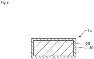
- Fig. 2 is a first view illustrating a manufacturing method for the semiconductor substrate 1 of the present embodiment.
- the manufacturing method for the semiconductor substrate 1 will be described.
- the metal member 20 is prepared.
- the conductive film 30 is formed on the prepared metal member 20.
- plating treatment using copper is performed on the metal member 20, and annealing treatment is performed to heat the metal member 20 that has undergone the plating treatment.
- the plating treatment and the annealing treatment are repeatedly performed twice.
- the member obtained by forming the conductive film 30 on the metal member 20 as shown in Fig. 2 is referred to as a plated member 1a, for convenience sake.
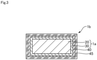
- Fig. 3 is a second view illustrating the manufacturing method for the semiconductor substrate 1 of the present embodiment.
- the barrier film 40 and the gold film 45 are formed on the surface of the plated member 1a.
- the barrier film 40 is formed by sputtering using platinum
- the gold film 45 is formed by sputtering using gold.
- a method for forming the barrier film 40 or the gold film 45 is not limited to sputtering, and may be plating treatment or vapor deposition.
- the member obtained by forming the barrier film 40 and the gold film 45 on the surface of the plated member 1a is referred to as a sputtered member 1b, for convenience sake.
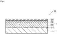
- Fig. 4 is a third view illustrating the manufacturing method for the semiconductor substrate 1 of the present embodiment.
- the nonmagnetic film 12 is formed on the prepared insulating member 11, separately from the manufacturing of the sputtered member 1b described in Fig. 2 and Fig. 3 .
- the titanium film 121, the copper film 122, the platinum film 123, and the gold film 124 are formed in this order on the surface 11a of the insulating member 11.
- the titanium film 121 is formed by sputtering using titanium
- the copper film 122 is formed by sputtering and plating using copper.
- the platinum film 123 is formed by vapor deposition using platinum
- the gold film 124 is formed by vapor deposition using gold.
- a method for forming the titanium film 121, the copper film 122, the platinum film 123, or the gold film 124 is not limited to sputtering or vapor deposition, and for example, a part of these films may be formed through plating treatment.
- Fig. 5 is a fourth view illustrating the manufacturing method of the semiconductor substrate 1 of the present embodiment.
- a gold-tin solder foil 50a is prepared separately from the sputtered member 1b and the base 10.
- the gold-tin solder foil 50a is interposed between the gold film 45 of the sputtered member 1b and the gold film 124 of the base 10 (blank arrows S1 and S2 in Fig. 5 ).
- these are heated in a reflow furnace with a nitrogen atmosphere or a hydrogen atmosphere.
- the sputtered member 1b and the base 10 are joined via the joining portion 50, whereby the semiconductor substrate 1 is manufactured.
- a method for joining the sputtered member 1b and the base 10 is not limited to the method using the gold-tin solder foil 50a, and a method of applying a gold-tin solder paste may be used.
- the conductive film 30 formed on the metal member 20 is made of copper which is the same material as the nonmagnetic material contained in the metal member 20.
- occurrence of a defect such as swell between the metal member 20 and the conductive film 30 is inhibited, whereby adhesion between the metal member 20 and the conductive film 30 is enhanced. Accordingly, it is possible to enhance adhesion between the base 10 and the metal member 20 joined via the conductive film 30 and the joining portion 50.
- the base 10 includes the insulating member 11 made of aluminum nitride which is a nonmagnetic material, and the nonmagnetic film 12 formed on the insulating member 11.
- the base 10 has a nonmagnetic property, and therefore, when the base 10 is joined to the metal member 20 having a nonmagnetic property, the semiconductor substrate 1 has a nonmagnetic property in its entirety. Accordingly, the semiconductor substrate 1 is less influenced by a magnetic field and therefore can be applied to fields in which a nonmagnetic property is needed.
- the semiconductor substrate 1 of the present embodiment includes the barrier film 40 formed between the conductive film 30 and the joining portion 50.
- gold atoms and tin atoms contained in the joining portion 50 can be inhibited from being dispersed into the conductive film 30.
- the metal member 20 is made of an alloy of tungsten and copper
- the conductive film 30 is made of copper which is the same material as the nonmagnetic material forming the metal member 20.
- the conductive film 30 becomes less likely to be separated from the metal member 20, so that adhesion between the metal member 20 and the conductive film 30 is enhanced. Accordingly, it is possible to enhance adhesion between the base 10 and the metal member 20 joined via the conductive film 30 and the joining portion 50.
- the conductive film 30 is to be formed on the metal member 20
- plating treatment using copper and annealing treatment of heating the film formed through plating treatment are performed a plurality of times.
- the residue of a plating liquid remaining at the film formed through the plating treatment evaporates and grain growth of copper is promoted, whereby adhesion between the metal member 20 and the conductive film 30 can be further enhanced. Accordingly, it is possible to enhance adhesion between the base 10 and the metal member 20 joined via the conductive film 30 and the joining portion 50.
- the present invention is not limited to the above embodiment and can be implemented in various embodiments without deviating from the gist of the present invention.
- the following modifications are also possible.
- the base 10 includes the insulating member 11 made of a nonmagnetic material, and the nonmagnetic film 12 formed on the insulating member 11.
- the configuration of the base 10 is not limited thereto, and the base 10 may include only the insulating member 11.
- the base 10 includes the insulating member 11 and the nonmagnetic film 12, and for example, the insulating member 11 is joined to the metal member 20 via the nonmagnetic film 12 and the joining portion 50, as shown in Fig. 1 .
- the joining manner between the insulating member 11 and the metal member 20 is not limited thereto.
- the insulating member 11 may be joined to the metal member 20 via the joining portion 50, on a side of the insulating member 11 where the nonmagnetic film 12 is not formed.
- the nonmagnetic material forming the insulating member 11 is not limited to aluminum nitride, and may not necessarily have an insulation property.
- the nonmagnetic material forming the insulating member 11 may be the same as or different from the nonmagnetic material contained in the metal member 20 or the joining portion 50.
- the semiconductor substrate 1 includes the barrier film 40, but the barrier film may be absent.
- Providing the barrier film 40 can inhibit gold atoms and tin atoms contained in the joining portion 50 from being dispersed into the conductive film 30.
- the metal member 20 is a heat sink made of an alloy of tungsten and copper.
- the material forming the metal member and the function of the metal member are not limited thereto. It suffices that the metal member contains a nonmagnetic material and has a nonmagnetic property.
- the conductive film 30 formed on the metal member 20 is formed by performing plating treatment and annealing treatment using copper on the metal member 20.
- a method for forming the conductive film 30 is not limited thereto.
- the conductive film 30 may be formed through sputtering or vapor deposition.
- a semiconductor substrate comprising:
Landscapes
- Engineering & Computer Science (AREA)
- Microelectronics & Electronic Packaging (AREA)
- Internal Circuitry In Semiconductor Integrated Circuit Devices (AREA)
- Chemical & Material Sciences (AREA)
- Ceramic Engineering (AREA)
- Materials Engineering (AREA)
- Cooling Or The Like Of Semiconductors Or Solid State Devices (AREA)
Abstract
Provided is a technology for enhancing adhesion between a base and a metal member in a semiconductor substrate. The semiconductor substrate includes: a base; a metal member containing a nonmagnetic material and having a nonmagnetic property; a conductive film formed on the metal member and made of the same material as the nonmagnetic material contained in the metal member; and a joining portion joining a side of the metal member where the conductive film is formed, to the base, the joining portion being made of a nonmagnetic material.
Description
- The present invention relates to a semiconductor substrate.
- Conventionally, there has been known a semiconductor substrate in which a metal member is joined to a base (for example,
Patent Documents 1 and 2). -
- Patent Document 1:
Japanese Patent No. 6629317 - Patent Document 2:
Japanese Patent No. 6883513 - However, even with conventional technologies as in
Patent Documents 1 and 2, there is still room for improvement regarding technology for enhancing adhesion between the base and the metal member in the semiconductor substrate. - An object of the present invention is to provide a technology for enhancing adhesion between a base and a metal member in a semiconductor substrate.
- The present invention has been made to solve at least one of the above problems and can be implemented as the following aspects.
- (1) One aspect of the present invention provides a semiconductor substrate. This semiconductor substrate includes: a base; a metal member containing a nonmagnetic material and having a nonmagnetic property; a conductive film formed on the metal member and made of the same material as the nonmagnetic material contained in the metal member; and a joining portion joining a side of the metal member where the conductive film is formed, to the base, the joining portion being made of a nonmagnetic material.
According to the above configuration, the conductive film formed on the metal member is made of the same material as the nonmagnetic material contained in the metal member. Thus, adhesion between the metal member and the conductive film is enhanced, whereby it is possible to enhance adhesion between the base and the metal member joined via the conductive film and the joining portion. - (2) In the semiconductor substrate of the above aspect, the base may include an insulating member made of a nonmagnetic material, and a nonmagnetic film formed on the insulating member. According to the above configuration, the base includes the insulating member made of a nonmagnetic material, and the nonmagnetic film formed on the insulating member, and therefore has a nonmagnetic property. Thus, the base having a nonmagnetic property and the metal member having a nonmagnetic property are joined via the joining portion made of a nonmagnetic material, whereby the semiconductor substrate has a nonmagnetic property. Accordingly, the entire semiconductor substrate is less influenced by a magnetic field and therefore can be applied to fields in which a nonmagnetic property is needed.
- (3) The semiconductor substrate of the above aspect may further include a barrier film formed between the conductive film and the joining portion. According to the above configuration, the barrier film formed between the conductive film and the joining portion can inhibit the material contained in the joining portion from being dispersed into the conductive film.
- (4) In the semiconductor substrate of the above aspect, the metal member may be made of an alloy of tungsten and copper, and the conductive film may be made of copper. According to the above configuration, the conductive film is formed of copper which is the nonmagnetic material forming the metal member. Thus, the conductive film becomes less likely to be separated from the metal member, so that adhesion between the metal member and the conductive film is enhanced. Accordingly, it is possible to enhance adhesion between the base and the metal member joined via the conductive film and the joining portion.
- The present invention can be implemented in various aspects. For example, the present invention can be implemented in aspects such as a semiconductor package including a semiconductor substrate, a manufacturing method for a semiconductor substrate, a computer program for executing manufacturing of a semiconductor substrate, and the like.
-
- [
Fig. 1 ] Sectional view of a semiconductor substrate of a first embodiment. - [
Fig. 2 ] First view illustrating a manufacturing method for the semiconductor substrate of the first embodiment. - [
Fig. 3 ] Second view illustrating a manufacturing method for the semiconductor substrate of the first embodiment. - [
Fig. 4 ] Third view illustrating a manufacturing method for the semiconductor substrate of the first embodiment. - [
Fig. 5 ] Fourth view illustrating a manufacturing method for the semiconductor substrate of the first embodiment. -
Fig. 1 is a sectional view of a semiconductor substrate of a first embodiment. Asemiconductor substrate 1 of the present embodiment is a substrate to which a semiconductor is mounted, and includes a heat sink for releasing heat generated at the semiconductor to outside. Thesemiconductor substrate 1 of the present embodiment is mainly used in a case where a nonmagnetic property is needed in a superconductive environment, e.g., in a quantum computer. Thesemiconductor substrate 1 includes abase 10, ametal member 20, aconductive film 30, abarrier film 40, and a joiningportion 50. InFig. 1 to Fig. 5 , the relationship of the thicknesses of thebase 10, themetal member 20, theconductive film 30, thebarrier film 40, and the joiningportion 50 is shown differently from an actual thickness relationship, for convenience of description. - The
base 10 includes aninsulating member 11 made of a nonmagnetic material, and anonmagnetic film 12 formed on theinsulating member 11. Thebase 10 supports themetal member 20 described later and the semiconductor (not shown). - The
insulating member 11 is a member having a flat-plate shape. The insulatingmember 11 is made of a nonmagnetic material having an insulation property, e.g., aluminum nitride (AlN), and has an insulating property. Here, "having an insulating property" means that an insulation resistance value is not less than 1.0×10⁸ Ω. The shape of the insulatingmember 11 is not limited thereto, and may be such a shape that can support themetal member 20 and the semiconductor. The nonmagnetic material forming the insulatingmember 11 is not limited to aluminum nitride. Oxide-based ceramic such as alumina (Al2O3), silica (SiO2), titania (HO2), or zirconia (ZrO2), nitride-based ceramic such as silicon nitride (SiN) or titanium nitride (TiN), or the like may be used. - The
nonmagnetic film 12 is formed on asurface 11a of theinsulating member 11. Thenonmagnetic film 12 includes atitanium film 121 made of titanium (Ti), acopper film 122 made of copper (Cu), aplatinum film 123 made of platinum (Pt), and agold film 124 made of gold (Au). In thenonmagnetic film 12 of the present embodiment, thetitanium film 121, thecopper film 122, theplatinum film 123, and thegold film 124 are laminated in this order from thesurface 11a side of theinsulating member 11. - The
base 10 includes theinsulating member 11 made of a nonmagnetic material, and thenonmagnetic film 12 made of metal that is a nonmagnetic material, and thus thebase 10 has a nonmagnetic property. Here, "having a nonmagnetic property" means having almost no magnetic property, and a small amount of magnetic material may be contained. In the present embodiment, a "member having a nonmagnetic property" is such a member that an average amount obtained by dividing the total amount of elements that exhibit a magnetic property, e.g., iron (Fe), nickel (Ni), cobalt (Co), and neodymium (Nd) contained in a plurality of measurement target areas set for the member, by the number of the measurement target areas, is not greater than a specific value. Specifically, using a scanning electron microscope (SEM) and an energy dispersive X-ray spectrometer (EDS), elemental analysis is performed for at least ten measurement target areas set on a surface or a cross-section of a member, under a predetermined measurement condition (magnification: 5000x, acceleration voltage of an electron gun: 20 kV, and a distance from the electron gun to the measurement target area: 10 mm). In the present embodiment, such a member that an average detection amount of elements that exhibit a magnetic property is not greater than 1.0 wt% as a result of the above elemental analysis is defined as a "member having a nonmagnetic property". Thebase 10 is a "member having a nonmagnetic property", in which an average detection amount of elements that exhibit a magnetic property is not greater than 1.0 wt%. - The
metal member 20 is a member containing a nonmagnetic material and having a nonmagnetic property. In the present embodiment, themetal member 20 is a heat sink made of an alloy of tungsten (W) and copper. Themetal member 20 has a function of releasing heat generated at the semiconductor mounted to thesemiconductor substrate 1, to outside. - The
conductive film 30 is formed on themetal member 20. Theconductive film 30 is made of the same material as the nonmagnetic material contained in themetal member 20. In the present embodiment, theconductive film 30 is made of copper, of tungsten and copper contained in themetal member 20. As shown inFig. 1 , theconductive film 30 is formed so as to coat the entirety of themetal member 20. On themetal member 20, a position where theconductive film 30 is formed is not limited to the above example. Theconductive film 30 may be formed only on a side joined to thebase 10 via the joiningportion 50. - The
barrier film 40 is formed between theconductive film 30 and the joiningportion 50 described later. In the present embodiment, thebarrier film 40 is made of platinum and is formed so as to coat the outer side of theconductive film 30. Thebarrier film 40 inhibits dispersion of gold atoms and tin atoms contained in the joiningportion 50. - A
gold film 45 is formed so as to coat the outer side of thebarrier film 40. Thegold film 45 is made of gold and assists joining between themetal member 20 and the joiningportion 50 via thebarrier film 40. - The joining
portion 50 joins a side of themetal member 20 where theconductive film 30 is formed, to thebase 10. The joiningportion 50 is made of a nonmagnetic material. In the present embodiment, the joiningportion 50 is solder made of gold and tin. The joiningportion 50 joins thebase 10 and themetal member 20. The nonmagnetic material forming the joiningportion 50 may be the same as or different from the nonmagnetic material contained in the insulatingmember 11 or themetal member 20. -
Fig. 2 is a first view illustrating a manufacturing method for thesemiconductor substrate 1 of the present embodiment. Here, the manufacturing method for thesemiconductor substrate 1 will be described. In the manufacturing method for thesemiconductor substrate 1, first, themetal member 20 is prepared. Next, theconductive film 30 is formed on theprepared metal member 20. Specifically, plating treatment using copper is performed on themetal member 20, and annealing treatment is performed to heat themetal member 20 that has undergone the plating treatment. In the present embodiment, the plating treatment and the annealing treatment are repeatedly performed twice. The member obtained by forming theconductive film 30 on themetal member 20 as shown inFig. 2 is referred to as a platedmember 1a, for convenience sake. -
Fig. 3 is a second view illustrating the manufacturing method for thesemiconductor substrate 1 of the present embodiment. After theconductive film 30 is formed on themetal member 20, thebarrier film 40 and thegold film 45 are formed on the surface of the platedmember 1a. In the present embodiment, thebarrier film 40 is formed by sputtering using platinum, and thegold film 45 is formed by sputtering using gold. A method for forming thebarrier film 40 or thegold film 45 is not limited to sputtering, and may be plating treatment or vapor deposition. The member obtained by forming thebarrier film 40 and thegold film 45 on the surface of the platedmember 1a is referred to as a sputteredmember 1b, for convenience sake. -
Fig. 4 is a third view illustrating the manufacturing method for thesemiconductor substrate 1 of the present embodiment. In the manufacturing method for thesemiconductor substrate 1, thenonmagnetic film 12 is formed on the prepared insulatingmember 11, separately from the manufacturing of the sputteredmember 1b described inFig. 2 andFig. 3 . Specifically, thetitanium film 121, thecopper film 122, theplatinum film 123, and thegold film 124 are formed in this order on thesurface 11a of the insulatingmember 11. In the present embodiment, thetitanium film 121 is formed by sputtering using titanium, and thecopper film 122 is formed by sputtering and plating using copper. Theplatinum film 123 is formed by vapor deposition using platinum, and thegold film 124 is formed by vapor deposition using gold. Thus, thebase 10 is manufactured. A method for forming thetitanium film 121, thecopper film 122, theplatinum film 123, or thegold film 124 is not limited to sputtering or vapor deposition, and for example, a part of these films may be formed through plating treatment. -
Fig. 5 is a fourth view illustrating the manufacturing method of thesemiconductor substrate 1 of the present embodiment. In the manufacturing method for thesemiconductor substrate 1, a gold-tin solder foil 50a is prepared separately from the sputteredmember 1b and thebase 10. The gold-tin solder foil 50a is interposed between thegold film 45 of the sputteredmember 1b and thegold film 124 of the base 10 (blank arrows S1 and S2 inFig. 5 ). In a state in which the gold-tin solder foil 50a is interposed between the sputteredmember 1b and thebase 10, these are heated in a reflow furnace with a nitrogen atmosphere or a hydrogen atmosphere. Thus, the sputteredmember 1b and the base 10 are joined via the joiningportion 50, whereby thesemiconductor substrate 1 is manufactured. A method for joining the sputteredmember 1b and thebase 10 is not limited to the method using the gold-tin solder foil 50a, and a method of applying a gold-tin solder paste may be used. - In the
semiconductor substrate 1 of the present embodiment described above, theconductive film 30 formed on themetal member 20 is made of copper which is the same material as the nonmagnetic material contained in themetal member 20. Thus, occurrence of a defect such as swell between themetal member 20 and theconductive film 30 is inhibited, whereby adhesion between themetal member 20 and theconductive film 30 is enhanced. Accordingly, it is possible to enhance adhesion between the base 10 and themetal member 20 joined via theconductive film 30 and the joiningportion 50. - In the
semiconductor substrate 1 of the present embodiment, thebase 10 includes the insulatingmember 11 made of aluminum nitride which is a nonmagnetic material, and thenonmagnetic film 12 formed on the insulatingmember 11. Thus, thebase 10 has a nonmagnetic property, and therefore, when thebase 10 is joined to themetal member 20 having a nonmagnetic property, thesemiconductor substrate 1 has a nonmagnetic property in its entirety. Accordingly, thesemiconductor substrate 1 is less influenced by a magnetic field and therefore can be applied to fields in which a nonmagnetic property is needed. - The
semiconductor substrate 1 of the present embodiment includes thebarrier film 40 formed between theconductive film 30 and the joiningportion 50. Thus, gold atoms and tin atoms contained in the joiningportion 50 can be inhibited from being dispersed into theconductive film 30. - In the
semiconductor substrate 1 of the present embodiment, themetal member 20 is made of an alloy of tungsten and copper, and theconductive film 30 is made of copper which is the same material as the nonmagnetic material forming themetal member 20. Thus, theconductive film 30 becomes less likely to be separated from themetal member 20, so that adhesion between themetal member 20 and theconductive film 30 is enhanced. Accordingly, it is possible to enhance adhesion between the base 10 and themetal member 20 joined via theconductive film 30 and the joiningportion 50. - In the manufacturing method for the
semiconductor substrate 1 of the present embodiment, when theconductive film 30 is to be formed on themetal member 20, plating treatment using copper and annealing treatment of heating the film formed through plating treatment are performed a plurality of times. Thus, the residue of a plating liquid remaining at the film formed through the plating treatment evaporates and grain growth of copper is promoted, whereby adhesion between themetal member 20 and theconductive film 30 can be further enhanced. Accordingly, it is possible to enhance adhesion between the base 10 and themetal member 20 joined via theconductive film 30 and the joiningportion 50. - The present invention is not limited to the above embodiment and can be implemented in various embodiments without deviating from the gist of the present invention. For example, the following modifications are also possible.
- In the above embodiment, it has been described that the
base 10 includes the insulatingmember 11 made of a nonmagnetic material, and thenonmagnetic film 12 formed on the insulatingmember 11. However, the configuration of thebase 10 is not limited thereto, and the base 10 may include only the insulatingmember 11. In the above embodiment, it has been described that thebase 10 includes the insulatingmember 11 and thenonmagnetic film 12, and for example, the insulatingmember 11 is joined to themetal member 20 via thenonmagnetic film 12 and the joiningportion 50, as shown inFig. 1 . However, the joining manner between the insulatingmember 11 and themetal member 20 is not limited thereto. The insulatingmember 11 may be joined to themetal member 20 via the joiningportion 50, on a side of the insulatingmember 11 where thenonmagnetic film 12 is not formed. The nonmagnetic material forming the insulatingmember 11 is not limited to aluminum nitride, and may not necessarily have an insulation property. The nonmagnetic material forming the insulatingmember 11 may be the same as or different from the nonmagnetic material contained in themetal member 20 or the joiningportion 50. - In the above embodiment, it has been described that the
semiconductor substrate 1 includes thebarrier film 40, but the barrier film may be absent. Providing thebarrier film 40 can inhibit gold atoms and tin atoms contained in the joiningportion 50 from being dispersed into theconductive film 30. - In the above embodiment, it has been described that the
metal member 20 is a heat sink made of an alloy of tungsten and copper. The material forming the metal member and the function of the metal member are not limited thereto. It suffices that the metal member contains a nonmagnetic material and has a nonmagnetic property. - In the above embodiment, it has been described that the
conductive film 30 formed on themetal member 20 is formed by performing plating treatment and annealing treatment using copper on themetal member 20. However, a method for forming theconductive film 30 is not limited thereto. Theconductive film 30 may be formed through sputtering or vapor deposition. - While the present aspect has been described above using the embodiment and modifications, the embodiment described above is merely for facilitating the understanding of the present aspect and is not intended to limit the present aspect. The present aspect may be subjected to change or modification without deviating from the gist thereof and the scope of the claims, and the present aspect includes equivalents thereof. Further, such technical features can be deleted as appropriate if not described as being essential in the present specification.
- A semiconductor substrate comprising:
- a base;
- a metal member containing a nonmagnetic material and having a nonmagnetic property;
- a conductive film formed on the metal member and made of the same material as the nonmagnetic material contained in the metal member; and
- a joining portion joining a side of the metal member where the conductive film is formed, to the base, the joining portion being made of a nonmagnetic material.
- The semiconductor substrate in accordance with application example 1, wherein
- the base includes
- an insulating member made of a nonmagnetic material, and
- a nonmagnetic film formed on the insulating member.
- The semiconductor substrate in accordance with application example 1 or 2, further comprising a barrier film formed between the conductive film and the joining portion.
- The semiconductor substrate in accordance with any one of application examples 1 to 3, wherein
- the metal member is made of an alloy of tungsten and copper, and
- the conductive film is made of copper.
-
- 1: semiconductor substrate
- 10: base
- 11: insulating member
- 12: nonmagnetic film
- 20: metal member
- 30: conductive film
- 40: barrier film
- 50: joining portion
- The present application is also directed to the following embodiments:
- [Embodiment 1] A semiconductor substrate(1) comprising:
- a base(10);
- a metal member(20) containing a nonmagnetic material and having a nonmagnetic property;
- a conductive film(30) formed on the metal member and made of the same material as the nonmagnetic material contained in the metal member; and
- a joining portion(50) joining a side of the metal member where the conductive film is formed, to the base, the joining portion being made of a nonmagnetic material.
- [Embodiment 2] The semiconductor substrate in accordance with
embodiment 1, wherein
the base includes- an insulating member(11) made of a nonmagnetic material, and
- a nonmagnetic film(12) formed on the insulating member.
- [Embodiment 3] The semiconductor substrate in accordance with
embodiment 1 or 2, further comprising a barrier film(40) formed between the conductive film and the joining portion. - [Embodiment 4] The semiconductor substrate in accordance with
embodiment 1 or 2, wherein- the metal member is made of an alloy of tungsten and copper, and
- the conductive film is made of copper.
Claims (5)
- A semiconductor substrate(1) comprising:a base(10);a metal member(20) containing a nonmagnetic material and having a nonmagnetic property;a conductive film(30) formed on the metal member and containing the same material as the nonmagnetic material contained in the metal member; anda joining portion(50) joining a side of the metal member where the conductive film is formed, to the base, the joining portion being made of a nonmagnetic material.
- The semiconductor substrate in accordance with claim 1, whereinthe base includesan insulating member(11) made of a nonmagnetic material, anda nonmagnetic film(12) formed on the insulating member.
- The semiconductor substrate in accordance with claim 1 or 2, further comprising a barrier film(40) formed between the conductive film and the joining portion.
- The semiconductor substrate in accordance with claim 1 or 2, whereinthe metal member is made of an alloy of tungsten and copper, andthe conductive film is made of copper.
- The semiconductor substrate in accordance with any one of claims 1 to 4, comprising:
a conductive film(30) formed on the metal member and made of the same material as the nonmagnetic material contained in the metal member.
Applications Claiming Priority (1)
| Application Number | Priority Date | Filing Date | Title |
|---|---|---|---|
| JP2023192391A JP2025079604A (en) | 2023-11-10 | 2023-11-10 | Semiconductor Substrate |
Publications (1)
| Publication Number | Publication Date |
|---|---|
| EP4554337A1 true EP4554337A1 (en) | 2025-05-14 |
Family
ID=93460778
Family Applications (1)
| Application Number | Title | Priority Date | Filing Date |
|---|---|---|---|
| EP24211712.5A Pending EP4554337A1 (en) | 2023-11-10 | 2024-11-08 | Substrate comprising a mounted semiconductor |
Country Status (6)
| Country | Link |
|---|---|
| US (1) | US20250157877A1 (en) |
| EP (1) | EP4554337A1 (en) |
| JP (1) | JP2025079604A (en) |
| KR (1) | KR20250069450A (en) |
| CN (1) | CN119993949A (en) |
| TW (1) | TW202537059A (en) |
Citations (4)
| Publication number | Priority date | Publication date | Assignee | Title |
|---|---|---|---|---|
| CN104209532B (en) * | 2014-03-19 | 2017-01-11 | 安泰天龙(天津)钨钼科技有限公司 | Thin tungsten copper sheet and preparing method of thin tungsten copper sheet |
| US20190103331A1 (en) * | 2014-10-31 | 2019-04-04 | General Electric Company | Non-magnetic package and method of manufacture |
| JP6883513B2 (en) | 2014-10-31 | 2021-06-09 | ゼネラル・エレクトリック・カンパニイ | Lids and methods for sealing non-magnetic packages |
| US20210313242A1 (en) * | 2018-11-13 | 2021-10-07 | Mitsubishi Electric Corporation | Semiconductor apparatus and semiconductor apparatus leak inspection method |
Family Cites Families (3)
| Publication number | Priority date | Publication date | Assignee | Title |
|---|---|---|---|---|
| JP2000269392A (en) * | 1998-09-04 | 2000-09-29 | Sumitomo Metal Electronics Devices Inc | Semiconductor module and heat dissipation insulating plate |
| JP2009158537A (en) * | 2007-12-25 | 2009-07-16 | Sumitomo Metal Electronics Devices Inc | Package for storing semiconductor elements |
| JP5245970B2 (en) * | 2009-03-26 | 2013-07-24 | 豊田合成株式会社 | LIGHT EMITTING DIODE, ITS MANUFACTURING METHOD, AND LAMP |
-
2023
- 2023-11-10 JP JP2023192391A patent/JP2025079604A/en active Pending
-
2024
- 2024-11-04 TW TW113142080A patent/TW202537059A/en unknown
- 2024-11-07 KR KR1020240157309A patent/KR20250069450A/en active Pending
- 2024-11-08 CN CN202411586575.6A patent/CN119993949A/en active Pending
- 2024-11-08 EP EP24211712.5A patent/EP4554337A1/en active Pending
- 2024-11-08 US US18/941,645 patent/US20250157877A1/en active Pending
Patent Citations (5)
| Publication number | Priority date | Publication date | Assignee | Title |
|---|---|---|---|---|
| CN104209532B (en) * | 2014-03-19 | 2017-01-11 | 安泰天龙(天津)钨钼科技有限公司 | Thin tungsten copper sheet and preparing method of thin tungsten copper sheet |
| US20190103331A1 (en) * | 2014-10-31 | 2019-04-04 | General Electric Company | Non-magnetic package and method of manufacture |
| JP6629317B2 (en) | 2014-10-31 | 2020-01-15 | ゼネラル・エレクトリック・カンパニイ | Non-magnetic package and manufacturing method |
| JP6883513B2 (en) | 2014-10-31 | 2021-06-09 | ゼネラル・エレクトリック・カンパニイ | Lids and methods for sealing non-magnetic packages |
| US20210313242A1 (en) * | 2018-11-13 | 2021-10-07 | Mitsubishi Electric Corporation | Semiconductor apparatus and semiconductor apparatus leak inspection method |
Also Published As
| Publication number | Publication date |
|---|---|
| TW202537059A (en) | 2025-09-16 |
| KR20250069450A (en) | 2025-05-19 |
| US20250157877A1 (en) | 2025-05-15 |
| CN119993949A (en) | 2025-05-13 |
| JP2025079604A (en) | 2025-05-22 |
Similar Documents
| Publication | Publication Date | Title |
|---|---|---|
| EP3196929B1 (en) | Method of manufacturing bonded body, method of manufacturing power module substrate with heat sink, and method of manufacturing heat sink | |
| EP3744705A1 (en) | Copper/ceramic bonded body, insulating circuit board, copper/ceramic bonded body production method, and insulating circuit board production method | |
| US4319264A (en) | Nickel-gold-nickel conductors for solid state devices | |
| EP3831799A1 (en) | Silicon nitride sintered body, silicon nitride substrate, and silicon nitride circuit substrate | |
| SG185508A1 (en) | Contact probe | |
| CN101266957A (en) | Semiconductor device and manufacturing method thereof | |
| US12112993B2 (en) | Heat radiation member | |
| US10790374B2 (en) | Method for forming ohmic contacts | |
| US12552722B2 (en) | Process for producing a metal-ceramic substrate, and a metal-ceramic substrate produced using such a method | |
| EP2958115A1 (en) | Oxide superconducting wire | |
| Moon et al. | Observed correlation of Sn oxide film to Sn whisker growth in Sn-Cu electrodeposit for Pb-free solders | |
| US20070117475A1 (en) | Prevention of Sn whisker growth for high reliability electronic devices | |
| US20250140733A1 (en) | Die bonding structure and method of manufacturing the same | |
| Gruber et al. | Refractory high entropy metal sublattice nitride thin films as diffusion barriers in Cu metallizations | |
| US20250157877A1 (en) | Semiconductor substrate | |
| EP4053091A1 (en) | Copper/ceramic assembly, insulated circuit board, method for producing copper/ceramic assembly, and method for producing insulated circuit board | |
| JPH04282836A (en) | Improvement of barrier in thin film laminate | |
| US20250098065A1 (en) | Bonded body and ceramic circuit board using same | |
| US20250087576A1 (en) | Bonded body, ceramic circuit board, semiconductor device, and method for manufacturing bonded body | |
| Wei et al. | Electromigration-induced Pb and Sn whisker growth in SnPb solder stripes | |
| JP7593764B2 (en) | Joint body and method for producing the same | |
| KR20220152386A (en) | Composites and heat dissipation members | |
| JP7330089B2 (en) | Silicon nitride substrate, silicon nitride circuit substrate and semiconductor device using the same | |
| JP7680556B2 (en) | Airtight Terminal | |
| US20250327172A1 (en) | Cobalt-titanium alloy sputtering target assembly and method of making |
Legal Events
| Date | Code | Title | Description |
|---|---|---|---|
| PUAI | Public reference made under article 153(3) epc to a published international application that has entered the european phase |
Free format text: ORIGINAL CODE: 0009012 |
|
| STAA | Information on the status of an ep patent application or granted ep patent |
Free format text: STATUS: REQUEST FOR EXAMINATION WAS MADE |
|
| 17P | Request for examination filed |
Effective date: 20241108 |
|
| AK | Designated contracting states |
Kind code of ref document: A1 Designated state(s): AL AT BE BG CH CY CZ DE DK EE ES FI FR GB GR HR HU IE IS IT LI LT LU LV MC ME MK MT NL NO PL PT RO RS SE SI SK SM TR |