EP4550971A1 - Integrated structure including diffusion barrier layer and electronic device including the same - Google Patents
Integrated structure including diffusion barrier layer and electronic device including the same Download PDFInfo
- Publication number
- EP4550971A1 EP4550971A1 EP24207980.4A EP24207980A EP4550971A1 EP 4550971 A1 EP4550971 A1 EP 4550971A1 EP 24207980 A EP24207980 A EP 24207980A EP 4550971 A1 EP4550971 A1 EP 4550971A1
- Authority
- EP
- European Patent Office
- Prior art keywords
- substrate
- diffusion barrier
- barrier layer
- metal
- structure according
- Prior art date
- Legal status (The legal status is an assumption and is not a legal conclusion. Google has not performed a legal analysis and makes no representation as to the accuracy of the status listed.)
- Pending
Links
Images



Classifications
-
- H—ELECTRICITY
- H10—SEMICONDUCTOR DEVICES; ELECTRIC SOLID-STATE DEVICES NOT OTHERWISE PROVIDED FOR
- H10D—INORGANIC ELECTRIC SEMICONDUCTOR DEVICES
- H10D8/00—Diodes
- H10D8/60—Schottky-barrier diodes
-
- H—ELECTRICITY
- H10—SEMICONDUCTOR DEVICES; ELECTRIC SOLID-STATE DEVICES NOT OTHERWISE PROVIDED FOR
- H10W—GENERIC PACKAGES, INTERCONNECTIONS, CONNECTORS OR OTHER CONSTRUCTIONAL DETAILS OF DEVICES COVERED BY CLASS H10
- H10W20/00—Interconnections in chips, wafers or substrates
- H10W20/40—Interconnections external to wafers or substrates, e.g. back-end-of-line [BEOL] metallisations or vias connecting to gate electrodes
- H10W20/41—Interconnections external to wafers or substrates, e.g. back-end-of-line [BEOL] metallisations or vias connecting to gate electrodes characterised by their conductive parts
- H10W20/425—Barrier, adhesion or liner layers
-
- H—ELECTRICITY
- H10—SEMICONDUCTOR DEVICES; ELECTRIC SOLID-STATE DEVICES NOT OTHERWISE PROVIDED FOR
- H10D—INORGANIC ELECTRIC SEMICONDUCTOR DEVICES
- H10D30/00—Field-effect transistors [FET]
- H10D30/60—Insulated-gate field-effect transistors [IGFET]
- H10D30/67—Thin-film transistors [TFT]
- H10D30/6729—Thin-film transistors [TFT] characterised by the electrodes
-
- H—ELECTRICITY
- H10—SEMICONDUCTOR DEVICES; ELECTRIC SOLID-STATE DEVICES NOT OTHERWISE PROVIDED FOR
- H10D—INORGANIC ELECTRIC SEMICONDUCTOR DEVICES
- H10D62/00—Semiconductor bodies, or regions thereof, of devices having potential barriers
- H10D62/80—Semiconductor bodies, or regions thereof, of devices having potential barriers characterised by the materials
- H10D62/82—Heterojunctions
-
- H—ELECTRICITY
- H10—SEMICONDUCTOR DEVICES; ELECTRIC SOLID-STATE DEVICES NOT OTHERWISE PROVIDED FOR
- H10D—INORGANIC ELECTRIC SEMICONDUCTOR DEVICES
- H10D62/00—Semiconductor bodies, or regions thereof, of devices having potential barriers
- H10D62/80—Semiconductor bodies, or regions thereof, of devices having potential barriers characterised by the materials
- H10D62/881—Semiconductor bodies, or regions thereof, of devices having potential barriers characterised by the materials being a two-dimensional material
- H10D62/883—Transition metal dichalcogenides, e.g. MoSe2
-
- H—ELECTRICITY
- H10—SEMICONDUCTOR DEVICES; ELECTRIC SOLID-STATE DEVICES NOT OTHERWISE PROVIDED FOR
- H10D—INORGANIC ELECTRIC SEMICONDUCTOR DEVICES
- H10D64/00—Electrodes of devices having potential barriers
- H10D64/01—Manufacture or treatment
- H10D64/011—Manufacture or treatment of electrodes ohmically coupled to a semiconductor
-
- H—ELECTRICITY
- H10—SEMICONDUCTOR DEVICES; ELECTRIC SOLID-STATE DEVICES NOT OTHERWISE PROVIDED FOR
- H10D—INORGANIC ELECTRIC SEMICONDUCTOR DEVICES
- H10D64/00—Electrodes of devices having potential barriers
- H10D64/01—Manufacture or treatment
- H10D64/012—Manufacture or treatment of electrodes comprising a Schottky barrier to a semiconductor
-
- H—ELECTRICITY
- H10—SEMICONDUCTOR DEVICES; ELECTRIC SOLID-STATE DEVICES NOT OTHERWISE PROVIDED FOR
- H10D—INORGANIC ELECTRIC SEMICONDUCTOR DEVICES
- H10D64/00—Electrodes of devices having potential barriers
- H10D64/01—Manufacture or treatment
- H10D64/012—Manufacture or treatment of electrodes comprising a Schottky barrier to a semiconductor
- H10D64/0121—Manufacture or treatment of electrodes comprising a Schottky barrier to a semiconductor to Group IV semiconductors
-
- H—ELECTRICITY
- H10—SEMICONDUCTOR DEVICES; ELECTRIC SOLID-STATE DEVICES NOT OTHERWISE PROVIDED FOR
- H10D—INORGANIC ELECTRIC SEMICONDUCTOR DEVICES
- H10D64/00—Electrodes of devices having potential barriers
- H10D64/60—Electrodes characterised by their materials
- H10D64/64—Electrodes comprising a Schottky barrier to a semiconductor
-
- H—ELECTRICITY
- H10—SEMICONDUCTOR DEVICES; ELECTRIC SOLID-STATE DEVICES NOT OTHERWISE PROVIDED FOR
- H10D—INORGANIC ELECTRIC SEMICONDUCTOR DEVICES
- H10D64/00—Electrodes of devices having potential barriers
- H10D64/60—Electrodes characterised by their materials
- H10D64/64—Electrodes comprising a Schottky barrier to a semiconductor
- H10D64/647—Schottky drain or source electrodes for IGFETs
-
- H—ELECTRICITY
- H10—SEMICONDUCTOR DEVICES; ELECTRIC SOLID-STATE DEVICES NOT OTHERWISE PROVIDED FOR
- H10P—GENERIC PROCESSES OR APPARATUS FOR THE MANUFACTURE OR TREATMENT OF DEVICES COVERED BY CLASS H10
- H10P14/00—Formation of materials, e.g. in the shape of layers or pillars
- H10P14/20—Formation of materials, e.g. in the shape of layers or pillars of semiconductor materials
- H10P14/34—Deposited materials, e.g. layers
- H10P14/3402—Deposited materials, e.g. layers characterised by the chemical composition
- H10P14/3436—Deposited materials, e.g. layers characterised by the chemical composition being chalcogenide semiconductor materials not being oxides, e.g. ternary compounds
-
- H—ELECTRICITY
- H10—SEMICONDUCTOR DEVICES; ELECTRIC SOLID-STATE DEVICES NOT OTHERWISE PROVIDED FOR
- H10W—GENERIC PACKAGES, INTERCONNECTIONS, CONNECTORS OR OTHER CONSTRUCTIONAL DETAILS OF DEVICES COVERED BY CLASS H10
- H10W20/00—Interconnections in chips, wafers or substrates
- H10W20/40—Interconnections external to wafers or substrates, e.g. back-end-of-line [BEOL] metallisations or vias connecting to gate electrodes
- H10W20/41—Interconnections external to wafers or substrates, e.g. back-end-of-line [BEOL] metallisations or vias connecting to gate electrodes characterised by their conductive parts
- H10W20/435—Cross-sectional shapes or dispositions of interconnections
Definitions
- the present invention relates to an integrated structure including a diffusion barrier layer, and more particularly, to an integrated structure including a diffusion barrier layer for reducing interface defects at a semiconductor-metal interface.
- NPU Neural Processing Unit
- CPU Central Processing Unit
- a metal-semiconductor interface is one of factors that may directly affect injection of electrons and output of current and determine performance of a semiconductor device, and a technique of reducing defects at the interface between a metal material used as an electrode or the like and a semiconductor channel, particularly, the metal-semiconductor interface formed by diffusion and intermixing of materials (atoms), is essential. Furthermore, unlike in the past, as the current semiconductor process technique is approaching the sub-nano (sub-1 nm) level, the design of quasi-ideal interfaces at the ultra-fine scale is very important to overcome the limitations of ultra-fine and highly integrated semiconductors in the future.
- the present invention has been made in view of the above problems, and it is an object of the present invention to provide an integrated structure that can control metal-semiconductor interface defects to overcome the limitations of ultra-fine and highly integrated semiconductors, and an electronic device including the same.
- an integrated structure comprising: a silicon or silicon-on-insulator (SOI) substrate; a conductive layer spaced apart from the substrate and including a metal or a metal compound; and a diffusion barrier layer provided between the substrate and the conductive layer.
- SOI silicon or silicon-on-insulator
- the substrate and the diffusion barrier layer may directly contact and form a van der Waals junction.
- the diffusion barrier layer may be a monolayer.
- the thickness of the diffusion barrier layer is 0.1 to 10 ⁇ .
- the diffusion barrier layer may include a transition metal dichalcogenide material.
- the transition metal dichalcogenide material may be expressed as chemical formula MX 2 , wherein M may be a transition metal element including Mo, W, Nb, V, Ta, Ti, Zr, Hf, Tc, Re, Ru, Co, Pd, Pt, Cu, Ga, In, Sn, Ge, Pb, or a combination of two or more selected from these, and X may be a chalcogen element including S, Se, Te, or a combination of two or more selected from these.
- M may be a transition metal element including Mo, W, Nb, V, Ta, Ti, Zr, Hf, Tc, Re, Ru, Co, Pd, Pt, Cu, Ga, In, Sn, Ge, Pb, or a combination of two or more selected from these
- X may be a chalcogen element including S, Se, Te, or a combination of two or more selected from these.
- the transition metal dichalcogenide material may include MoS 2 , MoSe 2 , MoTe 2 , WS 2 , WSe 2 , WTe 2 , ZrS 2 , ZrSe 2 , HfS 2 , HfSe 2 , NbSe 2 , ReSe 2 , PdTe 2 , or a combination of two or more selected from these.
- the crystal structure of the transition metal dichalcogenide material may be a hexagonal structure in a plane direction.
- the metal may include Ti, Ni, Cr/Au, Ag, or a combination of two or more selected from these.
- Movement of materials (atoms) between the conductive layer and the substrate may be blocked.
- Injection of electrons from the substrate to the conductive layer may be blocked.
- Injection of holes from the conductive layer to the substrate may be performed.
- An electronic device may include an integrated structure including any one selected from those described above.
- FIG. 1 is a mimetic view showing the cross-section of an integrated structure 100 having a diffusion barrier layer 20 according to an embodiment of the present invention.
- the integrated structure 100 may include a silicon or Silicon-on-insulator (SOI) substrate 10; a conductive layer 30 spaced apart from the substrate and including a metal or a metal compound; and a diffusion barrier layer 20 provided therebetween.
- the diffusion barrier layer 20 may be a thin film and perform a function of blocking movement of materials (atoms, electrons, and the like) between the substrate 10 and the conductive layer 30, for example, movement of metal atoms from the conductive layer 30 to the substrate 10.
- the substrate 10 may be a silicon or Silicon-on-insulator (SOI) substrate as a semiconductor material, and more specifically, may be a p-type silicon as a p-type semiconductor material.
- the substrate 10 may additionally use a material doped with a dopant, but it is not limited thereto.
- the conductive layer 30 may include a metal or a metal compound.
- the metal or metal compound may include a metal element including Ti, Ni, Cr/Au, Ag, or a combination of two or more selected from these, and any type that includes a metal element suitable for being applied as an electronic device, such as a metal electrode, metal interconnection, or the like, may be used without limitation.
- the substrate 10 and the diffusion barrier layer 20 may directly contact to form a van der Waals junction by van der Waals force (vdW).
- vdW van der Waals force
- the junction between the silicon lattice on the surface of the substrate 10 and the diffusion barrier layer 20 may be formed owing to bonding by the van der Waals force.
- Each interface is physically and distinctly separated while atoms in each layer are not interchangeably mixed with or penetrating each other, i.e., a van der Waals gap is formed between the substrate 10 and the diffusion barrier layer 20.
- a diffusion barrier layer 20 of uniform thickness may be formed while minimizing physical damage to the surface by applying a transfer process, more specifically, a wet transfer process.
- the diffusion barrier layer 20 formed by van der Waals bonding is provided on the surface of the substrate 10, highly reactive dangling bond on the surface of the substrate 10 is removed, and unique properties of the substrate 10 can be preserved, so that it can be advantageously applied to implementation of a highly integrated device.
- the diffusion barrier layer 20 and the conductive layer 30 may also directly contact, and the interface between these two may ideally form a van der Waals (vdW) junction, but in reality, it may include an intermixing region due to diffusion of metal atoms of the conductive layer 30 into the diffusion barrier layer 20 without forming the van der Waals (vdW) junction.
- vdW van der Waals
- the movement/diffusion of materials (atoms) between the substrate 10 and the conductive layer 30 may be controlled through the diffusion barrier layer 20, and through this, injection of electrons may be controlled.
- the conventional metal-semiconductor interface forming direct contact as metal atoms may diffuse or penetrate into the silicon crystal by a general deposition method that forms a metal electrode, an intermixing defect of heterogeneous elements may be formed.
- the diffusion barrier layer 20 the integrated structure according to the present invention may block diffusion of metal atoms from the conductive layer 30 into the lattice of the substrate 10 (e.g., metal --* Si direction).
- injection of holes from the conductive layer 30 toward the substrate 10 may be controlled through the diffusion barrier layer 20.
- the ON/OFF ratio which is the driving performance of the device, can be improved as much as more than 100 times. This is since that as formation of the metal-induced gap state by the penetration of metal atoms into the lattice of silicon (Si) is suppressed through the application of the diffusion barrier layer 20, the Fermi level according to voltage driving can be freely controlled without the Fermi level pinning phenomenon at the metal/semiconductor interface.
- hole injection efficiency can be improved by fundamentally eliminating the factors that hinder hole injection due to such a reason.
- the diffusion barrier layer 20 may be formed as a monolayer, and when one or more layers are repeatedly laminated to be formed as a multilayer of two or more layers, the hole injection efficiency may be lowered, and this may not be desirable.
- the thickness of the monolayer diffusion barrier layer 20 that enhances the hole injection efficiency may be as shallow as a nano to sub-nano scale or lower, and may be extremely thin as much as 1 nm or lower, and excellent characteristics can be maintained while the thickness is small.
- the thickness of the diffusion barrier layer 20 may be 0.1 to 10 ⁇ , specifically 0.3 to 9 ⁇ , and more specifically 0.5 to 8 ⁇ . In a specific example, the thickness of the diffusion barrier layer 20 may be 7 ⁇ , but it is not limited thereto.
- the diffusion barrier layer 20 like this may be advantageously applied to implementation of a highly integrated device having a fine line width.
- the diffusion barrier layer 20 may have a low resistivity value of about 10 -2 ⁇ cm or smaller, specifically about 10 -4 to 10 -2 ⁇ cm. Since the diffusion barrier layer 20 has low resistivity, it may have excellent electrical conductivity of a level similar to that of a metal or a semimetal. However, when the thickness of the diffusion barrier layer 20 is extremely thin, for example, 1 nm or lower, it may have a resistivity value of semiconductor level.
- the diffusion barrier layer 20 is a semiconductor material and may include a transition metal dichalcogenide (TMD) material.
- TMD transition metal dichalcogenide
- the transition metal dichalcogenide material may have a two-dimensional crystal structure and excellent diffusion protection properties, and various advantages such as being formed in a very small thickness and the like.
- the transition metal dichalcogenide (TMD) may be a material having n-type or p-type semiconductor properties without doping, and particularly, the transition metal dichalcogenide (TMD) may be a material having p-type semiconductor properties.
- an atomic substitution process may be additionally performed in the chalcogen atom layer.
- the transition metal dichalcogenide (TMD) layer having p-type semiconductor properties is in contact with the p-type silicon substrate 10, it may suppress insulator silicon oxide (SiO 2 ) that is formed by chemical bonding of silicon (Si) dangling bonds on the surface of the silicon substrate 10 with oxygen atoms in the air, and may also suppress direct diffusion of metal atoms of the conductive layer 30 into the silicon lattice and formation of silicide during the deposition process of the conductive layer 30, and thus it may fundamentally block the problem of inhomogeneity of the silicon substrate. Through this, formation of the metal-induced gap state due to the metal may be blocked in the silicon band structure, and the Fermi level pinning phenomenon can be suppressed ultimately.
- SiO 2 insulator silicon oxide
- Si silicon
- the transition metal dichalcogenide material may be expressed as chemical formula MX 2 , wherein M is a transition metal element and may include, for example, Mo, W, Nb, V, Ta, Ti, Zr, Hf, Tc, Re, Ru, Co, Pd, Pt, Cu, Ga, In, Sn, Ge, Pb, or a combination of two or more selected from these, and X is a chalcogen element may include S, Se, Te, or a combination of two or more selected from these.
- the transition metal dichalcogenide material may include MoS 2 , MoSe 2 , MoTe 2 , WS 2 , WSe 2 , WTe 2 , ZrS 2 , ZrSe 2 , HfS 2 , HfSe 2 , NbSe 2 , ReSe 2 , PdTe 2 , or a combination of two or more selected from these. More specifically, the transition metal dichalcogenide material may include MoS 2 , MoSe 2 , WS 2 , WSe 2 , or a combination of two or more selected from these, and may include WSe 2 in a specific example, but it is not limited thereto.
- the crystal structure of the transition metal dichalcogenide material has a covalent bond between the transition metal M and the chalcogen element X, and based on this, it has a hexagonal structure in the plane direction. It may also be possible to change the crystal structure through an additional phase change step or doping step.
- the diffusion barrier layer 20 may include a transition metal dichalcogenide (TMD) material, there is no dangling bond extending outside the diffusion barrier layer 20, so that when the diffusion barrier layer 20 is formed on the substrate 10, unique properties of the substrate 10 can be preserved, and it can be advantageously applied to implementation of a highly integrated device.
- TMD transition metal dichalcogenide
- FIG. 2 shows a result of photographing the cross-section of a metal-semiconductor interface using a transmission electron microscope (TEM), a result of element mapping on the cross-section thereof, and a result of EDS analysis, in an integrated structure according to an example of the present invention.
- TEM transmission electron microscope
- the metal (Ni) electrode forms a direct contact with the substrate without having a WSe 2 diffusion barrier layer
- FIG. 3 shows a mimetic view of the cross-section of a metal-diffusion barrier layer-semiconductor interface, a result of photographing the cross-section of the metal-diffusion barrier layer-semiconductor interface using a transmission electron microscope (TEM), and a result of EDS element mapping on the cross-section thereof, in an integrated structure according to an example of the present invention.
- TEM transmission electron microscope
- the distance between the two quartz boats is set to 40 cm, and the temperature of each heating zone is set to 870 °C in the left zone and 640 °C in the right zone, and WSe 2 is grown for 10 minutes.
- the flow rate of Ar/H 2 gas as carrier gas is 100/20 sccm, and the process pressure in the synthesis stage is optimized to 1 to 100 Torr.
- a PMMA (Poly (methyl methacrylate)) polymer solution is coated on the WSe 2 thin film grown on the silicon oxide (SiO 2 ) substrate manufactured in the method of Manufacturing Example 1.
- the manufactured PMMA/WSe 2 /SiO 2 is immersed in a 3 wt% KOH solution to separate the PMMA/WSe 2 layer and the SiO 2 substrate.
- a patterned silicon (Si) substrate is manufactured through a photo lithography process.
- the peeled PMMA/WSe 2 layer is transferred onto a p-type silicon (Si) substrate patterned through the photo lithography process, and the PMMA and photoresist (PR) are removed using acetone. Therefore, a WSe 2 thin film provided on a silicon (Si) substrate is manufactured using a wet transfer method, and a Si/WSe 2 interface having a van der Waals (vdW) junction is prepared.
- a Schottky diode and a silicon (Si) channel transistor are manufactured by including the Si/WSe 2 interface manufactured in the method of Manufacturing Example 2.
- a metal electrode is deposited by an e-beam evaporator.
- Ti, Ni, Cr/Au, or Ag is used as a metal that will be used as the metal electrode.
- a Schottky diode is manufactured by forming a metal electrode in a lift-off method of removing the patterned photoresist, which is progressed in the exposure process, using acetone.
- an Si channel transistor is manufactured in a back gating structure using a silicon on insulator (SOI) wafer.
- SOI silicon on insulator
- the Si/WSe 2 interface fabricated in the method of Manufacturing Example 2 is formed on a Si channel having a channel length of 10 ⁇ m and a width of 2 ⁇ m, and a WSe 2 layer is bonded directly underneath the Ni electrode by depositing the Ni electrode thereon using an electron beam evaporator.
- the van der Waals (vdW) junction may not be formed in reality due to the issues such as the process or the like, and as the surface of the WSe 2 layer is damaged, an intermixing region due to diffusion of Ni atoms into the WSe 2 layer may be included.
- the surface of the SOI wafer is lightly oxidized in a dry oxidation method using plasma, and then a metal (Ni) electrode is formed using a method the same as the lift-off method described above.
- a Schottky diode and a silicon (Si) channel transistor are manufactured using a method the same as that of the embodiment, except that the Si/WSe 2 interface manufactured in the method of Manufacturing Example 2 is not included.
- Test Example Measurement of Schottky diode and transistor including van der Waals (vdW)-bonded Si/WSe 2 interface
- the electrical characteristics of the Schottky diode are analyzed. Specifically, the I-V rectification characteristics, Schottky barrier height (SBH), and interface trap density D it are calculated to verify the effect of inserting the WSe 2 interfacial layer.
- the I-V rectification characteristics obtain the result of current (I) by applying a voltage (V) of -2 V to 2 V.
- Equation 1 q is the quantity of electric charge, V is the applied voltage, ⁇ is the ideality factor, k is the Boltzmann constant, and T is the temperature.
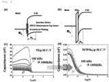
- FIG. 4 is a view showing (a, c) an energy diagram and a C-V graph of a metal-semiconductor interface, and (b, d) an energy diagram and a C-V graph of a metal-diffusion barrier layer-semiconductor interface, in an integrated structure according to an example of the present invention.
- FIG. 5 it shows an Si p-MOS device in which an electrode is formed as a WSe 2 and metal stacking structure on a silicon on insulator (SOI) substrate, and it can be confirmed that when drain voltage is applied, hole charges injected through the metal/WSe 2 electrode are transmitted through the silicon channel (Si channel) and the Si p-MOS device is driven.
- SOI silicon on insulator
Landscapes
- Electrodes Of Semiconductors (AREA)
Abstract
An integrated structure according to a preferred embodiment of the present invention may include a silicon or silicon-on-insulator (SOI) substrate, a conductive layer spaced apart from the substrate and including a metal or a metal compound, and a diffusion barrier layer provided therebetween. The substrate and the diffusion barrier layer may directly contact and form a van der Waals junction. Since the diffusion barrier layer may block diffusion of metal atoms into the substrate lattice by blocking movement of materials (atoms) between the substrate and the conductive layer and may also control injection of holes from the conductive layer toward the substrate, defects at the metal-semiconductor interface may be controlled to overcome the limitations of ultra-fine and highly integrated semiconductors.
Description
- The present invention relates to an integrated structure including a diffusion barrier layer, and more particularly, to an integrated structure including a diffusion barrier layer for reducing interface defects at a semiconductor-metal interface.
- In order to implement a technique of fusing artificial intelligence and Internet of Things (IoT), development of intelligent semiconductor synapse elements that may operate at a low power is actively conducted worldwide. In particular, for the sake of advancement in realistic non-contact industry and national safety networks in the post COVID-19 era, autonomous control devices for autonomously collecting, learning, determining, and processing information are required. In addition, the need for Neural Processing Unit (NPU) as an artificial intelligence semiconductor optimized for deep learning algorithm operations is emerging in the artificial intelligence techniques widely used in the 4th industry including big data analysis, autonomously driving vehicles, and the like, and since most of existing computing semiconductors centered on the Central Processing Unit (CPU) are expected to be replaced with NPUs, which are artificial intelligence semiconductors, importance of developing advanced semiconductors having driving performance capable of processing a large amount of information at a high speed and a low power is further emphasized.
- A metal-semiconductor interface is one of factors that may directly affect injection of electrons and output of current and determine performance of a semiconductor device, and a technique of reducing defects at the interface between a metal material used as an electrode or the like and a semiconductor channel, particularly, the metal-semiconductor interface formed by diffusion and intermixing of materials (atoms), is essential. Furthermore, unlike in the past, as the current semiconductor process technique is approaching the sub-nano (sub-1 nm) level, the design of quasi-ideal interfaces at the ultra-fine scale is very important to overcome the limitations of ultra-fine and highly integrated semiconductors in the future.
- Therefore, the present invention has been made in view of the above problems, and it is an object of the present invention to provide an integrated structure that can control metal-semiconductor interface defects to overcome the limitations of ultra-fine and highly integrated semiconductors, and an electronic device including the same.
- To accomplish the above object, according to one aspect of the present invention, there is provided an integrated structure comprising: a silicon or silicon-on-insulator (SOI) substrate; a conductive layer spaced apart from the substrate and including a metal or a metal compound; and a diffusion barrier layer provided between the substrate and the conductive layer.
- The substrate and the diffusion barrier layer may directly contact and form a van der Waals junction.
- The diffusion barrier layer may include a p-type semiconductor material.
- The diffusion barrier layer may be a monolayer.
- The thickness of the diffusion barrier layer is 0.1 to 10 Å.
- The diffusion barrier layer may include a transition metal dichalcogenide material.
- The transition metal dichalcogenide material may be expressed as chemical formula MX2, wherein M may be a transition metal element including Mo, W, Nb, V, Ta, Ti, Zr, Hf, Tc, Re, Ru, Co, Pd, Pt, Cu, Ga, In, Sn, Ge, Pb, or a combination of two or more selected from these, and X may be a chalcogen element including S, Se, Te, or a combination of two or more selected from these.
- The transition metal dichalcogenide material may include MoS2, MoSe2, MoTe2, WS2, WSe2, WTe2, ZrS2, ZrSe2, HfS2, HfSe2, NbSe2, ReSe2, PdTe2, or a combination of two or more selected from these.
- The crystal structure of the transition metal dichalcogenide material may be a hexagonal structure in a plane direction.
- The metal may include Ti, Ni, Cr/Au, Ag, or a combination of two or more selected from these.
- Movement of materials (atoms) between the conductive layer and the substrate may be blocked.
- Injection of electrons from the substrate to the conductive layer may be blocked.
- Injection of holes from the conductive layer to the substrate may be performed.
- An electronic device may include an integrated structure including any one selected from those described above.
-
-
FIG. 1 is a mimetic view showing the operation of a diffusion barrier layer in the cross-section of an integrated structure according to an embodiment of the present invention. -
FIG. 2 shows a result of photographing the cross-section of a metal-semiconductor interface using a transmission electron microscope (TEM), a result of EDS-based element mapping, and a result of analyzing information on the element of each component, in an integrated structure according to an example of the present invention. -
FIG. 3 shows a mimetic view of the cross-section of a metal-diffusion barrier layer-semiconductor interface, a result of photographing the cross-section of the metal-diffusion barrier layer-semiconductor interface using a transmission electron microscope (TEM), and a result of EDS-based element mapping, in an integrated structure according to an example of the present invention. -
FIG. 4 is a view showing (a, c) an energy diagram and a C-V graph of a metal-semiconductor interface, and (b, d) an energy diagram and a C-V graph of a metal-diffusion barrier layer-semiconductor interface, in an integrated structure according to an example of the present invention. -
FIG. 5 is a view showing (a) a mimetic view of an electronic device including an integrated structure, and (b) an I-V graph, (c) an On/Off ratio, and (d) maximum mobility according to the presence or absence of a diffusion barrier layer, in an integrated structure according to an example of the present invention. - Hereinafter, preferred embodiments of the present invention will be described in detail with reference to the accompanying drawings. The advantages and features of the present invention and the method for achieving them will become clear by referring to the embodiments described below in detail together with the accompanying drawings. However, the present invention is not limited to the embodiments disclosed below and will be implemented in various different forms. These embodiments are provided only to make the disclosure of the present invention complete and to fully inform those skilled in the art of the scope of the present invention, and the present invention is only defined by the scope of the claims. Like reference numerals refer to like elements throughout the specification.
- Unless defined otherwise, all the terms (including technical and scientific terms) used in this specification may be used as meanings that can be commonly understood by those skilled in the art. In addition, terms defined in commonly used dictionaries are not interpreted ideally or excessively unless clearly and specifically defined. The terms used in this specification are to describe the embodiments and are not to limit the present invention. In this specification, singular forms also include plural forms unless specifically stated otherwise in the phrases.
- The terms "comprises, includes" and/or "comprising, including" used in this specification means that the mentioned components, steps, operations, and/or elements do not exclude the presence or addition of one or more other components, steps, operations and/or elements.
- Integrated structure including a diffusion barrier layer
-
FIG. 1 is a mimetic view showing the cross-section of an integratedstructure 100 having adiffusion barrier layer 20 according to an embodiment of the present invention. - Referring to
FIG. 1 , the integratedstructure 100 may include a silicon or Silicon-on-insulator (SOI)substrate 10; aconductive layer 30 spaced apart from the substrate and including a metal or a metal compound; and adiffusion barrier layer 20 provided therebetween. Thediffusion barrier layer 20 may be a thin film and perform a function of blocking movement of materials (atoms, electrons, and the like) between thesubstrate 10 and theconductive layer 30, for example, movement of metal atoms from theconductive layer 30 to thesubstrate 10. - The
substrate 10 may be a silicon or Silicon-on-insulator (SOI) substrate as a semiconductor material, and more specifically, may be a p-type silicon as a p-type semiconductor material. Thesubstrate 10 may additionally use a material doped with a dopant, but it is not limited thereto. - The
conductive layer 30 may include a metal or a metal compound. The metal or metal compound may include a metal element including Ti, Ni, Cr/Au, Ag, or a combination of two or more selected from these, and any type that includes a metal element suitable for being applied as an electronic device, such as a metal electrode, metal interconnection, or the like, may be used without limitation. - The
substrate 10 and thediffusion barrier layer 20 may directly contact to form a van der Waals junction by van der Waals force (vdW). Specifically, the junction between the silicon lattice on the surface of thesubstrate 10 and thediffusion barrier layer 20 may be formed owing to bonding by the van der Waals force. Each interface is physically and distinctly separated while atoms in each layer are not interchangeably mixed with or penetrating each other, i.e., a van der Waals gap is formed between thesubstrate 10 and thediffusion barrier layer 20. In particular, in the process of manufacturing thediffusion barrier layer 20, adiffusion barrier layer 20 of uniform thickness may be formed while minimizing physical damage to the surface by applying a transfer process, more specifically, a wet transfer process. As thediffusion barrier layer 20 formed by van der Waals bonding is provided on the surface of thesubstrate 10, highly reactive dangling bond on the surface of thesubstrate 10 is removed, and unique properties of thesubstrate 10 can be preserved, so that it can be advantageously applied to implementation of a highly integrated device. - The
diffusion barrier layer 20 and theconductive layer 30 may also directly contact, and the interface between these two may ideally form a van der Waals (vdW) junction, but in reality, it may include an intermixing region due to diffusion of metal atoms of theconductive layer 30 into thediffusion barrier layer 20 without forming the van der Waals (vdW) junction. - The movement/diffusion of materials (atoms) between the
substrate 10 and theconductive layer 30 may be controlled through thediffusion barrier layer 20, and through this, injection of electrons may be controlled. In the conventional metal-semiconductor interface forming direct contact, as metal atoms may diffuse or penetrate into the silicon crystal by a general deposition method that forms a metal electrode, an intermixing defect of heterogeneous elements may be formed. However, as thediffusion barrier layer 20 is provided, the integrated structure according to the present invention may block diffusion of metal atoms from theconductive layer 30 into the lattice of the substrate 10 (e.g., metal --* Si direction). Accordingly, as formation of an intermixing junction by metal atoms diffusing into the silicon substrate crystal and formation of a silicide, which is a compound of silicon and metal, are suppressed, and the interface defect density is reduced, there is an effect of blocking electron injection in the reverse direction from thesubstrate 10 to the conductive layer 30 (e.g., in the direction of Si--*metal). According thereto, contact resistance at the interface between thesubstrate 10 and theconductive layer 30 is reduced, trap density is reduced, and height of the Schottky barrier is reduced. Accordingly, as a quasi-ideal interface may be formed by reducing leakage current of the electronic device and maximizing rectification characteristics through thediffusion barrier layer 20, there is an effect of improving electrical characteristics. - In addition, injection of holes from the
conductive layer 30 toward thesubstrate 10 may be controlled through thediffusion barrier layer 20. Specifically, as the efficiency of injecting holes from the metal of theconductive layer 30 toward the substrate 10 (e.g., metal --* Si direction) is improved through thediffusion barrier layer 20, the ON/OFF ratio, which is the driving performance of the device, can be improved as much as more than 100 times. This is since that as formation of the metal-induced gap state by the penetration of metal atoms into the lattice of silicon (Si) is suppressed through the application of thediffusion barrier layer 20, the Fermi level according to voltage driving can be freely controlled without the Fermi level pinning phenomenon at the metal/semiconductor interface. As a result, it can be explained that hole injection efficiency can be improved by fundamentally eliminating the factors that hinder hole injection due to such a reason. - In particular, in order to enhance the effect of hole injection efficiency, the
diffusion barrier layer 20 may be formed as a monolayer, and when one or more layers are repeatedly laminated to be formed as a multilayer of two or more layers, the hole injection efficiency may be lowered, and this may not be desirable. The thickness of the monolayerdiffusion barrier layer 20 that enhances the hole injection efficiency may be as shallow as a nano to sub-nano scale or lower, and may be extremely thin as much as 1 nm or lower, and excellent characteristics can be maintained while the thickness is small. The thickness of thediffusion barrier layer 20 may be 0.1 to 10 Å, specifically 0.3 to 9 Å, and more specifically 0.5 to 8 Å. In a specific example, the thickness of thediffusion barrier layer 20 may be 7 Å, but it is not limited thereto. Thediffusion barrier layer 20 like this may be advantageously applied to implementation of a highly integrated device having a fine line width. - In addition, the
diffusion barrier layer 20 may have a low resistivity value of about 10-2 Ω·cm or smaller, specifically about 10-4 to 10-2 Ω·cm. Since thediffusion barrier layer 20 has low resistivity, it may have excellent electrical conductivity of a level similar to that of a metal or a semimetal. However, when the thickness of thediffusion barrier layer 20 is extremely thin, for example, 1 nm or lower, it may have a resistivity value of semiconductor level. - The
diffusion barrier layer 20 is a semiconductor material and may include a transition metal dichalcogenide (TMD) material. The transition metal dichalcogenide material may have a two-dimensional crystal structure and excellent diffusion protection properties, and various advantages such as being formed in a very small thickness and the like. The transition metal dichalcogenide (TMD) may be a material having n-type or p-type semiconductor properties without doping, and particularly, the transition metal dichalcogenide (TMD) may be a material having p-type semiconductor properties. In order to enhance the doping characteristics, an atomic substitution process may be additionally performed in the chalcogen atom layer. - As the transition metal dichalcogenide (TMD) layer having p-type semiconductor properties is in contact with the p-
type silicon substrate 10, it may suppress insulator silicon oxide (SiO2) that is formed by chemical bonding of silicon (Si) dangling bonds on the surface of thesilicon substrate 10 with oxygen atoms in the air, and may also suppress direct diffusion of metal atoms of theconductive layer 30 into the silicon lattice and formation of silicide during the deposition process of theconductive layer 30, and thus it may fundamentally block the problem of inhomogeneity of the silicon substrate. Through this, formation of the metal-induced gap state due to the metal may be blocked in the silicon band structure, and the Fermi level pinning phenomenon can be suppressed ultimately. - The transition metal dichalcogenide material may be expressed as chemical formula MX2, wherein M is a transition metal element and may include, for example, Mo, W, Nb, V, Ta, Ti, Zr, Hf, Tc, Re, Ru, Co, Pd, Pt, Cu, Ga, In, Sn, Ge, Pb, or a combination of two or more selected from these, and X is a chalcogen element may include S, Se, Te, or a combination of two or more selected from these. Specifically, the transition metal dichalcogenide material may include MoS2, MoSe2, MoTe2, WS2, WSe2, WTe2, ZrS2, ZrSe2, HfS2, HfSe2, NbSe2, ReSe2, PdTe2, or a combination of two or more selected from these. More specifically, the transition metal dichalcogenide material may include MoS2, MoSe2, WS2, WSe2, or a combination of two or more selected from these, and may include WSe2 in a specific example, but it is not limited thereto.
- The crystal structure of the transition metal dichalcogenide material has a covalent bond between the transition metal M and the chalcogen element X, and based on this, it has a hexagonal structure in the plane direction. It may also be possible to change the crystal structure through an additional phase change step or doping step.
- In addition, when the
diffusion barrier layer 20 may include a transition metal dichalcogenide (TMD) material, there is no dangling bond extending outside thediffusion barrier layer 20, so that when thediffusion barrier layer 20 is formed on thesubstrate 10, unique properties of thesubstrate 10 can be preserved, and it can be advantageously applied to implementation of a highly integrated device. -
FIG. 2 shows a result of photographing the cross-section of a metal-semiconductor interface using a transmission electron microscope (TEM), a result of element mapping on the cross-section thereof, and a result of EDS analysis, in an integrated structure according to an example of the present invention. - Referring to
FIG. 2 , in the integrated structure in which the metal (Ni) electrode forms a direct contact with the substrate without having a WSe2 diffusion barrier layer, it can confirm that the metal element (Ni) and the oxygen (O) element simultaneously exist in the interfacial layer that is in contact with the substrate as the metal atoms diffuse or penetrate into the silicon crystal, and therefore, it can be known that an intermixing region is formed by mixing heterogeneous elements. -
FIG. 3 shows a mimetic view of the cross-section of a metal-diffusion barrier layer-semiconductor interface, a result of photographing the cross-section of the metal-diffusion barrier layer-semiconductor interface using a transmission electron microscope (TEM), and a result of EDS element mapping on the cross-section thereof, in an integrated structure according to an example of the present invention. - Referring to
FIG. 3 , it can be confirmed that in the integrated structure in which the Si/WSe2 interface is constructed by providing a WSe2 diffusion barrier layer and metal (Ag) is laminated, an intermixing region is not formed as metal atoms do not diffuse or penetrate into silicon crystal. - Hereinafter, the present invention will be described in more detail using embodiments and comparative examples. However, the embodiments and comparative examples described below are intended to illustrate the present invention, and the scope of the present invention is not limited thereto.
- To synthesize tungsten diselenide (WSe2), a chemical vapor deposition (CVD) device provided with two heating zones is used. First, silicon oxide (SiO2) is used as the substrate, and a quartz boat containing 480 mg of selenium (Se, 99.5% Sigma-Aldrich) powder is disposed in the left heating zone, and a quartz boat containing mixed powder of 40 mg of NaCl (99%, Sigma-Aldrich) and 240 mg of tungsten oxide (WOx, 99.9%, Sigma-Aldrich) is disposed in the right heating zone. Thereafter, the distance between the two quartz boats is set to 40 cm, and the temperature of each heating zone is set to 870 °C in the left zone and 640 °C in the right zone, and WSe2 is grown for 10 minutes. At this point, the flow rate of Ar/H2 gas as carrier gas is 100/20 sccm, and the process pressure in the synthesis stage is optimized to 1 to 100 Torr.
- A PMMA (Poly (methyl methacrylate)) polymer solution is coated on the WSe2 thin film grown on the silicon oxide (SiO2) substrate manufactured in the method of Manufacturing Example 1. After PMMA coating, the manufactured PMMA/WSe2/SiO2 is immersed in a 3 wt% KOH solution to separate the PMMA/WSe2 layer and the SiO2 substrate. Meanwhile, a patterned silicon (Si) substrate is manufactured through a photo lithography process. The peeled PMMA/WSe2 layer is transferred onto a p-type silicon (Si) substrate patterned through the photo lithography process, and the PMMA and photoresist (PR) are removed using acetone. Therefore, a WSe2 thin film provided on a silicon (Si) substrate is manufactured using a wet transfer method, and a Si/WSe2 interface having a van der Waals (vdW) junction is prepared.
- A Schottky diode and a silicon (Si) channel transistor are manufactured by including the Si/WSe2 interface manufactured in the method of Manufacturing Example 2. After an exposure process of patterning a metal electrode on the substrate including the Si/WSe2 interface is progressed, a metal electrode is deposited by an e-beam evaporator. At this point, Ti, Ni, Cr/Au, or Ag is used as a metal that will be used as the metal electrode. Then, a Schottky diode is manufactured by forming a metal electrode in a lift-off method of removing the patterned photoresist, which is progressed in the exposure process, using acetone.
- Meanwhile, an Si channel transistor is manufactured in a back gating structure using a silicon on insulator (SOI) wafer. The Si/WSe2 interface fabricated in the method of Manufacturing Example 2 is formed on a Si channel having a channel length of 10 µm and a width of 2 µm, and a WSe2 layer is bonded directly underneath the Ni electrode by depositing the Ni electrode thereon using an electron beam evaporator. Here, although it is ideal to form the WSe2/Ni interface as a van der Waals (vdW) junction, the van der Waals (vdW) junction may not be formed in reality due to the issues such as the process or the like, and as the surface of the WSe2 layer is damaged, an intermixing region due to diffusion of Ni atoms into the WSe2 layer may be included. After patterning the channel through a photo lithography process, the surface of the SOI wafer is lightly oxidized in a dry oxidation method using plasma, and then a metal (Ni) electrode is formed using a method the same as the lift-off method described above.
- A Schottky diode and a silicon (Si) channel transistor are manufactured using a method the same as that of the embodiment, except that the Si/WSe2 interface manufactured in the method of Manufacturing Example 2 is not included.
- In order to analyze the effect of reducing the defects at the metal/semiconductor interface by forming the WSe2 interface at the metal/semiconductor interface, the electrical characteristics of the Schottky diode are analyzed. Specifically, the I-V rectification characteristics, Schottky barrier height (SBH), and interface trap density Dit are calculated to verify the effect of inserting the WSe2 interfacial layer. The I-V rectification characteristics obtain the result of current (I) by applying a voltage (V) of -2 V to 2 V. The current of the Schottky diode may be generally determined by Equation 1 shown below.

- In equation 1, q is the quantity of electric charge, V is the applied voltage, η is the ideality factor, k is the Boltzmann constant, and T is the temperature. In addition, saturation current I0 is as shown in
equation 2.
- In
equation 2, A is the diode area, A* is the Richardson constant, T is the temperature, q is the quantity of electric charge, k is the Boltzmann constant, and φ0 is the Schottky barrier height (SBH). Through this, it can be seen that variables constituting the saturation current I0 are the temperature T and the Schottky barrier height φ0. Using this, saturation current is measured at seven temperature points at 10 °C intervals from room temperature (RT, 25 °C) to 75 °C, and the Schottky barrier height is calculated. Since the current flow in an actual Schottky diode is dominantly determined by the current flowing due to a low SBH, it may be correctively calculated through the Barrier Height Inhomogeneities (BHI) model that compensates for the Schottky barrier height. - Since charge trap is mainly generated by interface defects, change in the interface defects may be indirectly inferred through the change in trap density. In addition, since the trap at the interface captures and releases charges, change in the trap density is quantitatively calculated by performing C-V (Capacitance-Voltage) and G-V (Conductance-Voltage) measurements. The C-V and G-V measurements obtain the changes in capacitance and conductance by fixing the frequency in units of 100 kHz from 100 kHz to 1 MHz and applying an AC voltage from -2 V to 2 V. The trap density Dit may be quantitatively expressed by Equation 3 shown below.

- In equation 3, A is the diode area, q is the quantity of electric charge, G is the conductance, and ω is the angular frequency.
-
FIG. 4 is a view showing (a, c) an energy diagram and a C-V graph of a metal-semiconductor interface, and (b, d) an energy diagram and a C-V graph of a metal-diffusion barrier layer-semiconductor interface, in an integrated structure according to an example of the present invention. - Referring to
FIGS. 4 (a) and (c) , at the metal-semiconductor interface forming a direct contact, as metal atoms may diffuse or penetrate into the silicon crystal by a general deposition method of forming a metal electrode, an intermixing defect of heterogeneous elements may be formed. Due to the intermixing defect, the intrinsic properties of the silicon (Si) substrate are modified, and a metal-induced gap state (MIGS) is formed in the silicon (Si) bandgap, which may generate a problem of causing a Fermi level pinning phenomenon when electrostatic actuation is driven through a gate. As a result, contact resistance of the metal-semiconductor interface increases, output current decreases, and the driving voltage of a device including the same increases, so that stress of the interface increases and may lead to degradation of the device. - Meanwhile, referring to
FIGS. 4 (b) and (d) , as the effect of inserting a diffusion barrier layer WSe2 between the substrate and the metal, decrease in the height of the Schottky barrier and decrease in the interface trap density Dit are confirmed. As a result of measuring the capacitance-voltage, it is confirmed that the defect density is reduced as the trap density Dit is reduced as much as more than 10 times after inserting WSe2. In addition, decrease in the defect density is confirmed to be similar to the result described above even in various metals such as Ni, Ti, Au/Cr, Ag, and the like which can be used as an electrode. -
FIG. 5 is a view showing (a) a mimetic view of an electronic device (Si p-MOS) having an integrated structure, (b) an I-V graph according to the presence or absence of a diffusion barrier layer, (c) an On/Off ratio, and (d) statistical results of maximum mobility, in an integrated structure according to an example of the present invention. - Referring to
FIG. 5 , it shows an Si p-MOS device in which an electrode is formed as a WSe2 and metal stacking structure on a silicon on insulator (SOI) substrate, and it can be confirmed that when drain voltage is applied, hole charges injected through the metal/WSe2 electrode are transmitted through the silicon channel (Si channel) and the Si p-MOS device is driven. - According to the present invention as described above, an integrated structure according to a preferred embodiment of the present invention may include a silicon or Silicon-on-insulator (SOI) substrate, a conductive layer spaced apart from the substrate and including a metal or a metal compound, and a diffusion barrier layer provided therebetween. The substrate and the diffusion barrier layer may directly contact to form a van der Waals junction. Since the diffusion barrier layer may block diffusion of metal atoms into the substrate lattice by blocking movement of materials (atoms) between the substrate and the conductive layer and may also control injection of holes from the conductive layer toward the substrate, defects at the metal-semiconductor interface may be controlled to overcome the limitations of ultra-fine and highly integrated semiconductors.
- The effects of the present invention are not limited to the effects mentioned above, and unmentioned other effects will be clearly understood by those skilled in the art from the following description.
- Although the embodiments of the present invention have been described above with reference to the accompanying drawings, those skilled in the art may understand that the present invention can be implemented in other specific forms without changing the technical spirit or essential features. Therefore, the embodiments described above should be understood as illustrative and not restrictive in all respects.
- 100: Integrated structure, 10: Substrate, 20: Diffusion barrier layer, 30: Conductive layer
Claims (13)
- An integrated structure comprising:a silicon or silicon-on-insulator (SOI) substrate;a conductive layer spaced apart from the substrate and including a metal or a metal compound; anda diffusion barrier layer provided between the substrate and the conductive layer, whereinthe substrate and the diffusion barrier layer directly contact and form a van der Waals junction.
- The structure according to claim 1, wherein the diffusion barrier layer includes a p-type semiconductor material.
- The structure according to claim 1, wherein the diffusion barrier layer is a monolayer.
- The structure according to claim 1, wherein a thickness of the diffusion barrier layer is 0.1 to 10 Å.
- The structure according to claim 1, wherein the diffusion barrier layer includes a transition metal dichalcogenide material.
- The structure according to claim 5, wherein the transition metal dichalcogenide material is expressed as chemical formula MX2, wherein
M is a transition metal element including Mo, W, Nb, V, Ta, Ti, Zr, Hf, Tc, Re, Ru, Co, Pd, Pt, Cu, Ga, In, Sn, Ge, Pb, or a combination of two or more selected from these, and X is a chalcogen element including S, Se, Te, or a combination of two or more selected from these. - The structure according to claim 5, wherein the transition metal dichalcogenide material includes MoS2, MoSe2, MoTe2, WS2, WSe2, WTe2, ZrS2, ZrSe2, HfS2, HfSe2, NbSe2, ReSe2, PdTe2, or a combination of two or more selected from these.
- The structure according to claim 5, wherein a crystal structure of the transition metal dichalcogenide material is a hexagonal structure in a plane direction.
- The structure according to claim 1, wherein the metal includes Ti, Ni, Cr/Au, Ag, or a combination of two or more selected from these.
- The structure according to claim 1, wherein movement of materials (atoms) between the conductive layer and the substrate is blocked.
- The structure according to claim 1, wherein injection of electrons from the substrate to the conductive layer is blocked.
- The structure according to claim 1, wherein injection of holes from the conductive layer to the substrate is performed.
- An electronic device comprising an integrated structure including any one selected from claims 1 to 12.
Applications Claiming Priority (1)
| Application Number | Priority Date | Filing Date | Title |
|---|---|---|---|
| KR1020230151913A KR102739804B1 (en) | 2023-11-06 | 2023-11-06 | Integrated structure including diffusion barrier layer and electronic device including the same |
Publications (1)
| Publication Number | Publication Date |
|---|---|
| EP4550971A1 true EP4550971A1 (en) | 2025-05-07 |
Family
ID=93257538
Family Applications (1)
| Application Number | Title | Priority Date | Filing Date |
|---|---|---|---|
| EP24207980.4A Pending EP4550971A1 (en) | 2023-11-06 | 2024-10-22 | Integrated structure including diffusion barrier layer and electronic device including the same |
Country Status (4)
| Country | Link |
|---|---|
| US (1) | US12278187B1 (en) |
| EP (1) | EP4550971A1 (en) |
| JP (1) | JP7675471B1 (en) |
| KR (1) | KR102739804B1 (en) |
Families Citing this family (1)
| Publication number | Priority date | Publication date | Assignee | Title |
|---|---|---|---|---|
| CN120730796B (en) * | 2025-08-29 | 2026-01-06 | 比亚迪股份有限公司 | A power device and its fabrication method, and an electronic device. |
Citations (2)
| Publication number | Priority date | Publication date | Assignee | Title |
|---|---|---|---|---|
| US20170033003A1 (en) * | 2015-07-31 | 2017-02-02 | Samsung Electronics Co., Ltd. | Multilayer structure including diffusion barrier layer and device including the multilayer structure |
| US20190148493A1 (en) * | 2015-05-20 | 2019-05-16 | Samsung Electronics Co., Ltd. | Semiconductor device including metal-2 dimensional material-semiconductor contact |
Family Cites Families (12)
| Publication number | Priority date | Publication date | Assignee | Title |
|---|---|---|---|---|
| KR20170000107A (en) * | 2015-06-23 | 2017-01-02 | 연세대학교 산학협력단 | p-n diode comprising two-dimensional semiconductor material and manufacturing method thereof |
| KR101732943B1 (en) * | 2015-06-25 | 2017-05-24 | 한국과학기술연구원 | A light-emitting diode having transition metal dichalcogen compound of two-dimensional(2D) structure as light-emitting layer and its preparing process |
| US10777410B2 (en) * | 2017-02-03 | 2020-09-15 | University Of South Carolina | Synthesis and fabrication of transition metal dichalcogenide structures |
| JP6896305B2 (en) | 2017-11-09 | 2021-06-30 | 国立研究開発法人産業技術総合研究所 | Semiconductor devices and their manufacturing methods |
| US11276644B2 (en) | 2018-12-17 | 2022-03-15 | Intel Corporation | Integrated circuits and methods for forming thin film crystal layers |
| US11043454B2 (en) | 2019-01-17 | 2021-06-22 | Samsung Electronics Co., Ltd. | Low resistivity interconnects with doped barrier layer for integrated circuits |
| JP2020123612A (en) | 2019-01-29 | 2020-08-13 | 株式会社半導体エネルギー研究所 | Semiconductor device manufacturing method and semiconductor device manufacturing apparatus |
| US11362180B2 (en) * | 2019-12-19 | 2022-06-14 | Taiwan Semiconductor Manufacturing Co., Ltd. | Semiconductor device and manufacturing method thereof |
| US11430666B2 (en) | 2019-12-31 | 2022-08-30 | Taiwan Semiconductor Manufacturing Co., Ltd. | Semiconductor device and method of manufacturing semiconductor device |
| KR102958407B1 (en) * | 2020-11-05 | 2026-04-27 | 삼성전자주식회사 | Semiconductor device including surface-treated semiconductor layer |
| CN114429988B (en) * | 2022-01-28 | 2022-08-23 | 北京科技大学 | Metal semiconductor contact structure based on two-dimensional semi-metal electrode |
| TWI861758B (en) * | 2023-03-13 | 2024-11-11 | 國立清華大學 | Two-dimensional semiconductor device and electrode used therein |
-
2023
- 2023-11-06 KR KR1020230151913A patent/KR102739804B1/en active Active
-
2024
- 2024-10-22 EP EP24207980.4A patent/EP4550971A1/en active Pending
- 2024-10-31 JP JP2024192207A patent/JP7675471B1/en active Active
- 2024-11-01 US US18/934,307 patent/US12278187B1/en active Active
Patent Citations (2)
| Publication number | Priority date | Publication date | Assignee | Title |
|---|---|---|---|---|
| US20190148493A1 (en) * | 2015-05-20 | 2019-05-16 | Samsung Electronics Co., Ltd. | Semiconductor device including metal-2 dimensional material-semiconductor contact |
| US20170033003A1 (en) * | 2015-07-31 | 2017-02-02 | Samsung Electronics Co., Ltd. | Multilayer structure including diffusion barrier layer and device including the multilayer structure |
Non-Patent Citations (1)
| Title |
|---|
| PATANIYA PRATIK M ET AL: "Photovoltaic activity of WSe2/Si hetero junction", MATERIALS RESEARCH BULLETIN, ELSEVIER, KIDLINGTON, GB, vol. 120, 24 August 2019 (2019-08-24), XP085831150, ISSN: 0025-5408, [retrieved on 20190824], DOI: 10.1016/J.MATERRESBULL.2019.110602 * |
Also Published As
| Publication number | Publication date |
|---|---|
| JP2025078609A (en) | 2025-05-20 |
| US12278187B1 (en) | 2025-04-15 |
| KR102739804B1 (en) | 2024-12-09 |
| JP7675471B1 (en) | 2025-05-13 |
Similar Documents
| Publication | Publication Date | Title |
|---|---|---|
| EP2164094B1 (en) | A method for reducing fermi-level-pinning in a non-silicon channel MOS device | |
| Maldonado et al. | Electrical properties of junctions between Hg and Si (111) surfaces functionalized with short-chain alkyls | |
| Bilgili et al. | Current-voltage characteristics of Ag/TiO2/n-InP/Au Schottky barrier diodes | |
| US12278187B1 (en) | Integrated structure having a P-type semiconductor diffusion barrier layer forming a Van Der Waals junction with a P-type substrate and electronic device including the same | |
| Bakkaloğlu et al. | Temperature dependence of electrical parameters of the Cu/n-Si metal semiconductor Schottky structures | |
| Yüksel et al. | A detailed analysis of current-voltage characteristics of Au/perylene-monoimide/n-Si Schottky barrier diodes over a wide temperature range | |
| Tyagi et al. | Analysis of interface states in Zn/p-NiO Schottky barrier diode | |
| Fukata et al. | Interaction of boron and phosphorus impurities in silicon nanowires during low-temperature ozone oxidation | |
| Weinberger et al. | The passivation of electrically active sites on the surface of crystalline silicon by fluorination | |
| Sovizi et al. | Detailed work function and structural investigations of layered MoO3 onto SiO2 and MoS2 in air | |
| US20240313080A1 (en) | Two-dimensional semiconductor device and electrode used therein | |
| Şahin et al. | Comparison of electrical properties of pure and copper-doped diamond-like carbon interfacial-layered Schottky devices under different temperature conditions | |
| Bhattacharya et al. | An alternative approach to extract diode parameters from metal–semiconductor–metal asymmetric Schottky diodes | |
| Alarabi et al. | Comparison of p-n and p-i-n vertical diodes based on p-PMItz/n-Si, p-PMItz/n-4HSiC and p-PMItz/i-SiO2/n-Si heterojunctions | |
| Mallikarjuna et al. | Photovoltaic and Barrier Properties of Au/n-Ge Schottky Junction Modified by Methylene Blue Organic Dye Interlayer | |
| Yadav et al. | Colloidal synthesized cobalt nanoparticles for nonvolatile memory device application | |
| Tao | Removal of surface states on Si (1 0 0) by valence-mending passivation | |
| Shekhawat et al. | Analysis of temperature sensitive electrical performance of sputter grown Ni and Ni–Cr Schottky contacts on 4 H-SiC | |
| Balcı et al. | On the electrical parameters, conduction mechanisms depend on temperature and voltage, and thermal sensor applications in the Re/n‑GaAs/Au Schottky diodes | |
| Su et al. | Temperature dependence of current–voltage characteristics of MoS2/Si devices prepared by the chemical vapor deposition method | |
| Anwar et al. | Temperature dependent characteristics of graphene/silicon Schottky junction | |
| Kumar | Ohmic contacts to homoepitaxially grown p-type and n-type germanium | |
| Al-Turk | Electronic Transport in Mixed-dimensional van der Waals Heterostructures | |
| Saad | Manufacturing and electrical characterization of MOS devices of ultrathin silicon dioxide layer | |
| Pham et al. | Detection of DNA of genetically modified maize by a silicon nanowire field-effect transistor |
Legal Events
| Date | Code | Title | Description |
|---|---|---|---|
| PUAI | Public reference made under article 153(3) epc to a published international application that has entered the european phase |
Free format text: ORIGINAL CODE: 0009012 |
|
| STAA | Information on the status of an ep patent application or granted ep patent |
Free format text: STATUS: REQUEST FOR EXAMINATION WAS MADE |
|
| 17P | Request for examination filed |
Effective date: 20241022 |
|
| AK | Designated contracting states |
Kind code of ref document: A1 Designated state(s): AL AT BE BG CH CY CZ DE DK EE ES FI FR GB GR HR HU IE IS IT LI LT LU LV MC ME MK MT NL NO PL PT RO RS SE SI SK SM TR |
|
| STAA | Information on the status of an ep patent application or granted ep patent |
Free format text: STATUS: EXAMINATION IS IN PROGRESS |
|
| 17Q | First examination report despatched |
Effective date: 20250708 |