EP4550084A1 - Elektronische vorrichtung mit tastenknopf - Google Patents
Elektronische vorrichtung mit tastenknopf Download PDFInfo
- Publication number
- EP4550084A1 EP4550084A1 EP24787398.7A EP24787398A EP4550084A1 EP 4550084 A1 EP4550084 A1 EP 4550084A1 EP 24787398 A EP24787398 A EP 24787398A EP 4550084 A1 EP4550084 A1 EP 4550084A1
- Authority
- EP
- European Patent Office
- Prior art keywords
- electronic device
- housing
- disposed
- plate
- wire member
- Prior art date
- Legal status (The legal status is an assumption and is not a legal conclusion. Google has not performed a legal analysis and makes no representation as to the accuracy of the status listed.)
- Pending
Links
Images


Classifications
-
- G—PHYSICS
- G06—COMPUTING OR CALCULATING; COUNTING
- G06F—ELECTRIC DIGITAL DATA PROCESSING
- G06F1/00—Details not covered by groups G06F3/00 - G06F13/00 and G06F21/00
- G06F1/16—Constructional details or arrangements
- G06F1/1613—Constructional details or arrangements for portable computers
- G06F1/1615—Constructional details or arrangements for portable computers with several enclosures having relative motions, each enclosure supporting at least one I/O or computing function
- G06F1/1616—Constructional details or arrangements for portable computers with several enclosures having relative motions, each enclosure supporting at least one I/O or computing function with folding flat displays, e.g. laptop computers or notebooks having a clamshell configuration, with body parts pivoting to an open position around an axis parallel to the plane they define in closed position
-
- G—PHYSICS
- G06—COMPUTING OR CALCULATING; COUNTING
- G06F—ELECTRIC DIGITAL DATA PROCESSING
- G06F1/00—Details not covered by groups G06F3/00 - G06F13/00 and G06F21/00
- G06F1/16—Constructional details or arrangements
- G06F1/1613—Constructional details or arrangements for portable computers
- G06F1/1633—Constructional details or arrangements of portable computers not specific to the type of enclosures covered by groups G06F1/1615 - G06F1/1626
- G06F1/1662—Details related to the integrated keyboard
- G06F1/1669—Detachable keyboards
-
- G—PHYSICS
- G06—COMPUTING OR CALCULATING; COUNTING
- G06F—ELECTRIC DIGITAL DATA PROCESSING
- G06F3/00—Input arrangements for transferring data to be processed into a form capable of being handled by the computer; Output arrangements for transferring data from processing unit to output unit, e.g. interface arrangements
- G06F3/01—Input arrangements or combined input and output arrangements for interaction between user and computer
- G06F3/02—Input arrangements using manually operated switches, e.g. using keyboards or dials
- G06F3/0202—Constructional details or processes of manufacture of the input device
-
- H—ELECTRICITY
- H01—ELECTRIC ELEMENTS
- H01H—ELECTRIC SWITCHES; RELAYS; SELECTORS; EMERGENCY PROTECTIVE DEVICES
- H01H13/00—Switches having rectilinearly-movable operating part or parts adapted for pushing or pulling in one direction only, e.g. push-button switch
- H01H13/70—Switches having rectilinearly-movable operating part or parts adapted for pushing or pulling in one direction only, e.g. push-button switch having a plurality of operating members associated with different sets of contacts, e.g. keyboard
- H01H13/86—Switches having rectilinearly-movable operating part or parts adapted for pushing or pulling in one direction only, e.g. push-button switch having a plurality of operating members associated with different sets of contacts, e.g. keyboard characterised by the casing, e.g. sealed casings or casings reducible in size
-
- H—ELECTRICITY
- H01—ELECTRIC ELEMENTS
- H01H—ELECTRIC SWITCHES; RELAYS; SELECTORS; EMERGENCY PROTECTIVE DEVICES
- H01H2209/00—Layers
- H01H2209/012—Layers avoiding too large deformation or stress
-
- H—ELECTRICITY
- H01—ELECTRIC ELEMENTS
- H01H—ELECTRIC SWITCHES; RELAYS; SELECTORS; EMERGENCY PROTECTIVE DEVICES
- H01H2211/00—Spacers
- H01H2211/006—Individual areas
- H01H2211/016—Wires
-
- H—ELECTRICITY
- H01—ELECTRIC ELEMENTS
- H01H—ELECTRIC SWITCHES; RELAYS; SELECTORS; EMERGENCY PROTECTIVE DEVICES
- H01H2223/00—Casings
- H01H2223/034—Bezel
-
- H—ELECTRICITY
- H01—ELECTRIC ELEMENTS
- H01H—ELECTRIC SWITCHES; RELAYS; SELECTORS; EMERGENCY PROTECTIVE DEVICES
- H01H2233/00—Key modules
- H01H2233/03—Key modules mounted on support plate or frame
Definitions
- Embodiments of the disclosure relate to an electronic device that includes a key button.
- Electronic devices are released with various functions and sizes according to user preferences, and may include a key button device including multiple key buttons as input means.Due to the use characteristic of such a key button device in which the key buttons should be hit with a certain load, an assembly structure and a fixing structure that take rigidity and/or support into consideration may be required when the key button device is fixed to a housing.
- An electronic device may include multiple key buttons arranged at predetermined intervals as input means. These key buttons may be arranged to be exposed to the outside from a housing and may be used to input data by being physically pressed by hitting.An electronic device including key buttons may be used by being communicatively connected to an external electronic device (e.g., a tablet PC or a laptop PC).
- the electronic device including the key buttons may include a Bluetooth keyboard device that is wirelessly connected to a portable electronic device such as a tablet PC or a laptop PC, which does not have physical key input means or is inconvenient to use physical key input means.
- the electronic device including the key buttons may include a keyboard device used as data input components for a desktop PC.
- the multiple key buttons may be arranged to be at least partially exposed from the inside of the housing to the outside through multiple openings provided in the housing.
- the multiple key buttons may be assembled by arranging the key buttons on a plate (e.g., a key button plate or a keyboard module) and fixing the plate to the housing.
- the plate is fixed to the housing through fastening members such as multiple screws and/or rivets around each of the multiple key buttons, thereby protecting against deformation or damage caused by hitting each key button.
- the multiple screws and/or rivets which should be placed around each of the multiple key buttons may increase work time when assembling or maintaining the electronic device, which may cause a decrease in productivity.
- rivets used as fastening members make disassembly difficult during maintenance, necessitating replacement of the entire key button assembly, which may increase maintenance costs.
- Various embodiments of the disclosure may provide an electronic device including a key button with an easy assembly structure.
- Various embodiments may provide an electronic device including a key button that is advantageous for maintenance and is capable of helping improve productivity.
- Various embodiments may provide an electronic device including a key button that is capable of helping improve the operational reliability of the electronic device by providing a stable support structure.
- an electronic device includes a housing including multiple protruding pin members, a plate coupled to the housing and including multiple through holes through which the multiple pin members pass, respectively, and a wire member disposed to support at least a portion of each of the multiple pin members protruding from the through holes.
- the plate is supported by the wire member.
- An electronic device includes an assembly structure in which, when assembling a plate (e.g., a keyboard module) including key buttons to a housing, the pin members penetrating from the housing penetrate the plate, and the plate is fixed to the housing so that the penetrated pin members are commonly supported by at least one wire member, which may help improve productivity and reduce manufacturing costs by reducing assembly time and number of components, and may help make repairs faster and reduce costs during maintenance.
- a uniform support force is provided via a support structure that seamlessly supports adjacent key buttons by a wire member, which may help improve the operational reliability of the electronic device.
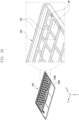
- FIG. 1 is a perspective view illustrating an electronic device according to various embodiments of the disclosure.
- the electronic device 200 may include a housing 201 including a front surface 200a oriented in a first direction (e.g., the z-axis direction), a rear surface oriented in a second direction (e.g., the -z-axis direction) opposite to the front surface 200a, and input members disposed in the inner space of the housing 201 to be at least partially exposed to at least a portion of the front surface 200a.
- the input members may include multiple key buttons disposed in a first area 202 (e.g., a button placement area) of the housing 201 to be at least partially exposed to the outside through the front surface 200a, and at least one key pad 236 disposed in a second area 203 (e.g., a key pad placement area) adjacent to the first area 202 to be at least partially exposed to the outside through the front surface 200a.
- the multiple key buttons 235 may be disposed to be spaced apart from each other at a predetermined interval.
- the illustrated electronic device 200 may be used as data input means by being wirelessly and/or wiredly connected to an external electronic device (e.g., a tablet PC or a laptop PC).
- an external electronic device e.g., a tablet PC or a laptop PC.
- the electronic device 200 may include a Bluetooth keyboard device that is wirelessly connected to an external electronic device.
- the electronic device 200 may include a wire member (e.g., the wire member 240 in FIG. 2 ) as a fixing structure that fixes a plate (e.g., the plate 230 in FIG. 2 ) (e.g., a key button plate or a keyboard module) on which multiple key buttons 235 are disposed, to the housing 201.
- a wire member e.g., the wire member 240 in FIG. 2
- the wire member may help improve productivity by replacing multiple fastening members such as screws or rivets, thereby simplifying an assembly process and reducing manufacturing costs.
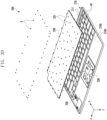
- FIG. 2 is an exploded perspective view of the electronic device according to various embodiments of the disclosure.
- the electronic device 200 may include a front surface cover 210 (e.g., a first cover or a first plate), a rear surface cover 220 (e.g., a second cover or a second plate) coupled to the front surface cover 210, a plate 230 (e.g., a keyboard module) disposed in the inner between the front surface cover 210 and the rear surface cover 220, and including multiple key buttons (e.g., the key buttons 235 in FIG.
- a front surface cover 210 e.g., a first cover or a first plate
- a rear surface cover 220 e.g., a second cover or a second plate
- a plate 230 e.g., a keyboard module
- the electronic device 200 may include multiple fastening members S (e.g., screws) for fixing at least a portion of the plate 230 to the front surface cover 210.
- the front surface cover 210 may include a first surface 210a facing the front surface (e.g., the front surface 200a in FIG. 1 ) of the electronic device 200, and a second surface 210b oriented in the opposite direction to the first surface 210a (e.g., the front side 200a in FIG. 1 ) (e.g., the -z-axis direction).
- the front surface cover 210 may include multiple openings OP disposed to accommodate multiple key buttons (e.g., the key buttons 235 in FIG.
- the front surface cover 210 may include the multiple pin members 211, each of which is fixed to the second surface 210b between adjacent ones of the multiple openings OP.
- the multiple pin members 211 may be made of a metal material, and may be fixed by being pressed into fixing grooves (e.g., the fixing grooves 215 in FIG.
- the multiple pin members 211 may be made of polymer (e.g., PC). In some embodiments, the multiple pin members 211 may be formed integrally with the front surface cover 210. In an embodiment, the front surface cover 210 and/or the rear surface cover 220 may be formed of a metal material or polymer. In some embodiments, the front surface cover 210 and/or the rear surface cover 220 may be formed to include both a metal material and a polymer through injection molding.
- the plate 230 may include multiple through holes 231.
- the multiple through holes 231 may be provided at corresponding positions to allow the multiple pin members 211 to pass therethrough, respectively, when the plate 230 is mounted on the second surface 210b of the front surface cover 210.
- the plate 230 may include a board (e.g., a printed board assembly (PBA)) on which multiple key buttons (e.g., the key buttons 235 in FIG. 1 ) are disposed.
- PBA printed board assembly
- the plate 230 is a separate support plate that supports the board on which the key buttons (e.g., the key buttons 235 in FIG. 1 ) are disposed, and may be made of a metal material and/or a polymer material.
- the wire member 240 may be disposed to support multiple pin members 211 protruding from the surface of the plate 230 after the plate 230 is mounted on the second surface 210b of the front surface cover 210.
- the wire member 240 may at least partially support the multiple pin members 211 protruding from the plate 230 from the plate 230, thereby reducing the deformation of the plate 230 caused by hitting the key buttons (e.g., the key buttons 235 in FIG.
- the wire member 240 may include a non-elastic metal wire.
- the wire member 240 may be made of a non-elastic carbon material, nylon material, fiber material, or heat-resistant fabric material.
- the multiple fastening members S may be disposed along the edge (e.g., the periphery) of the plate 230, and may assist in fixing the plate 230 by being fastened to the second surface 210b of the front surface cover 210 after penetrating the plate 230.
- the electronic device 200 may include a tension maintaining structure 250 that is disposed on the second surface 210b and, in the state in which one end of the wire member 240 is fixed to the front surface cover 210, pulls tightly the other end of the wire member 240 to firmly support the multiple members 211.
- the wire member 240 may support the multiple pin members 211 in a tight state without sagging through the tension maintaining structure 250.
- FIGS. 3A to 3M an assembly process of the electronic device will be described through FIGS. 3A to 3M .
- FIG. 3A is a perspective view of a front surface cover according to various embodiments of the disclosure.
- FIG. 3B is a perspective view of the front surface cover to which pin members are fixed according to various embodiments of the disclosure.
- FIG. 3C is a view illustrating a process of fixing a pin member according to various embodiments of the disclosure.
- the front surface cover 210 may include multiple openings OP penetrating it from the first surface 210a to the second surface 210b.
- the multiple openings OP may be arranged at a predetermined interval and may cause at least some of the multiple key buttons (e.g., the key buttons 235 in FIG. 1 ) disposed on the plate (e.g., the plate 230 in FIG.
- the front surface cover 210 may include multiple fixing grooves 215, each of which is provided between adjacent ones of the multiple openings OP, on the second surface 210b.
- the multiple fixing grooves 215 may be formed together when forming the front surface cover 210, or may be formed on the front surface cover 210 through post-processing.
- the multiple pin members 211 may be fixed to the multiple fixing grooves 215.
- the multiple pin members 211 may be fixed to protrude from the second surface 210b by a predetermined height.
- each of the multiple pin members 211 may include a post 2111 (e.g., a shaft portion) having a predetermined length, and a head 2112 provided at an end of the post 2111 to have a larger diameter than the post 2111.
- the wire member e.g., the wire member 240 in FIG.
- each of the multiple pin members 211 may further include a bearing member 2113 disposed to surround at least a portion of the post 2111.
- the bearing member 2113 may be rotatably disposed relative to the post 2111.
- the bearing member 2113 may be replaced with a metal ring longitudinally cut and rotatably disposed to surround the post.
- (a) of FIG. 3C is a view illustrating a state in which the bearing member 2113 is mounted on the pin member 211, (b) of FIG.
- FIG. 3C is a view illustrating a state in which the pin member 211 having the bearing member 2113 mounted thereon is mounted in a fixing groove 215 of the front surface cover 210
- (c) of FIG. 3C is a view illustrating a state in which the pin member 211 having the bearing member 2113 mounted thereon is fixed to the fixing groove 215 of the front surface cover 210.
- the wire member when the wire member (e.g., the wire member 240 in FIG. 2 ) is disposed to support the multiple pin members 211, the wire member (e.g., the wire member 240 in FIG. 2 ) may be disposed to be in contact with at least a portion of the bearing member 2113.
- the multiple pin members 211 may be fixed by being press-fitted into the fixing grooves 215 formed at a predetermined depth on the second surface 210b of the front surface cover 210 using a press jig.
- the multiple pin members 211 may be arranged at intervals of about 30 mm to 35 mm (preferably, 32.5 mm) along the row direction of openings OP (e.g., the first to fifth rows R1 to R5 in FIG. 3G ) to prevent the plate 230 from being permanently deformed or sagging when the key buttons (e.g., the key buttons 235 in FIG. 1 ) are hit.
- the multiple pin members 211 may be provided in a screw type in which the pin members 211 are partially threaded so as to be fastened to screw grooves formed at a predetermined depth on the second surface 210b of the front surface cover 210.
- the pin members 211 may be formed integrally with the front surface cover 210.
- the electronic device 200 may include a plate 230 mounted on the front surface cover 210 in the state in which the multiple pin members 211 are fixed.
- the plate 230 may include multiple through holes 231.
- the multiple pin members 211 disposed to protrude from the second surface 210b may pass through the multiple through holes 231 in the plate 230 and then protrude from the surface of the plate 230.
- the plate 230 may be fixed to the second surface 210b of the front surface cover 210 by multiple fastening members S (e.g., screws) disposed along the edge thereof.
- the plate 230 may be fixed along areas A, B, C, and D areas in FIG. 3F , which are edge areas (e.g., peripheral areas) of the plate 230 by the multiple fastening members S.
- FIG. 3G is a view illustrating a state in which a wire member is applied to a plate according to various embodiments of the disclosure.
- FIG. 3H is an enlarged view illustrating the area 3h of FIG. 3G according to various embodiments of the disclosure.
- FIG. 3I is a view illustrating a state in which one end of a wire member is fixed in the area 3i of FIG. 3H according to various embodiments of the disclosure.
- FIG. 3J is a partial cross-sectional view of the electronic device according to various embodiments of the disclosure taken along line 3j-3j in FIG. 3H .
- FIG. 3K is a partial cross-sectional view of the electronic device according to various embodiments of the disclosure taken along line 3k-3k in FIG. 3H .
- FIG. 3L is a partial cross-sectional view of the electronic device according to various embodiments of the disclosure taken along line 3I-3I in FIG. 3H .
- FIG. 3M is a partial cross-sectional view of an electronic device viewed along line 3m-3m of FIG. 3H according to various embodiments of the disclosure.
- the electronic device 200 may include a wire member 240 disposed to support multiple pin members 211 protruding from the surface of the plate 230 mounted on the second surface 210b of the front surface cover 210.
- one end 241 of the wire member 240 may be fixed to a fixing groove 215a formed in the second surface 210b of the front surface cover 210 by a fastening member S, and the other end (e.g., the other end 242 in FIG. 4B ) may be pulled in a first direction (e.g., in direction 1 FIG. 3G ) by the tension maintaining structure 250, thereby supporting the multiple pin members 211 while maintaining tight tension.
- the multiple pin members 211 may be arranged along the rows R1, R2, R3, R4, and R5 in the horizontal direction (e.g., the x-axis direction) to correspond to the arrangement of the key buttons (e.g., the key buttons 235 in FIG.
- the multiple pin members 211 may be arranged along a first row R1, a second row R2 arranged in parallel with the first row R1, a third row R3 arranged in parallel with the second row R2, a fourth row R4 arranged in parallel with the third row R3, and a fifth row R5 arranged in parallel with the fourth row R4.
- the number of rows R1, R2, R3, R4, and R5 is not limited, and may be changed in various ways depending on the arrangement order of key buttons (e.g., the key buttons 235 in FIG. 1 ) applied to the electronic device 200.
- the wire member 240 may be disposed to support the multiple pin members 211 along the first row R1, and then support the multiple pin members 211 in the order of the second row R2, the third row R3, the fourth row R4, and the fifth row R5.
- the wire member 240 may maintain tighter tension, and separation of the wire member due to an external impact may be reduced when the wire member 240 is disposed such that a pressing direction for supporting a first pin member 211a among the multiple pin members 211 and a direction for pressing a second pin member 211b adjacent to the first pin member 211a are opposite to each other.
- the wire member 240 may be disposed to press the post 2111 of the first pin member 211a in a second direction (e.g., direction 2 in FIG. 3H ) on one side of the first pin member 211a among the multiple pin members 211.
- the wire member 240 may be prevented from being separated by the head 2112 of the first pin member 211a.
- the wire member 240 may be disposed to press the post 2111 of the second pin member 211b in a third direction (e.g., direction 3 in FIG.
- the wire member 240 may be prevented from being separated by the head 2112 of the second pin member 211b.
- the wire members 240 may be disposed sequentially along respective rows R1, R2, R3, R4, and R5 to press adjacent pin members 211 in opposite directions in the manner described above, and may finally be fixed to the tension maintaining structure 250.
- the wire member 240 since the wire member 240 is disposed to support the bearing member 2113 rotatably coupled to the post 2111 of each pin member 211, the wire member 240 may be smoothly pulled in the first direction (e.g., direction 1) by the tension maintaining structure 250, thereby maintaining tight tension.
- the bearing member 2113 may rotate counterclockwise.
- the bearing member 2113 may rotate clockwise.
- the wire member 240 may be disposed to at least partially press the multiple pin members 211, and in a state in which tight tension is maintained by the tension maintaining structure 250, the wire member 240 may support the plate 230 while being in contact with the surface of the plate 230.
- the difference between the diameter d1 of the wire member 240 and the distance d2 between the head (e.g., the head 2112) of the pin member (e.g., the first pin member 211a) and the plate 230 may be 0.5 mm or less.
- the wire member 240 may be disposed to maintain the distance d2 between the head (e.g., the head 2112) of the pin member (e.g., the first pin member 211a) and the plate 230.
- the diameter d1 of the wire member 240 may be substantially equal to the distance d2 between the head (e.g., the head 2112) of the pin member (e.g., the first pin member 211a) and the plate 230.
- the support structure of the plate 230 based on fastening members such as conventional screws disposed around the key buttons 235 may not be provided with a separate support structure between the fastening members
- the support structure of the plate 203 based on the wire member 240 supports the plate 230 seamlessly from the first pin member 211a to the adjacent second pin member 211b, which may help reduce permanent deformation of the plate 230 and/or the front surface cover 210 caused by hitting the key buttons 235.
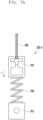
- FIG. 4A is a perspective view of a tension maintaining structure according to various embodiments of the disclosure.
- FIGS. 4B and 4C are views each illustrating a state in which the other end of a wire member is elastically coupled by the tension maintaining structure according to various embodiments of the disclosure.
- the tension maintaining structure 250 may be disposed on a second surface 210b of a front surface cover 210.
- the tension maintaining structure 250 may be disposed to provide tension that tightly pulls the other end 242 of the wire member 240 disposed to support multiple pin members 211.
- the tension maintaining structure 250 may include a fixing member 251 fixed to the second surface 210b of the front surface cover 210, a slide member slidably coupled to the fixing member 251 and fixing the other end 242 of the wire member 240, and an elastic member 253 elastically interconnecting the fixing member 251 and the slide member 252.
- the slide member 252 may be disposed on the second surface 210b of the front surface cover 210, or may be disposed to be capable of reciprocating along a guide rail 216 formed integrally with the second surface 210b.
- the elastic member 253 may include a rubber band.
- the other end 242 of the wire member 240 may be fixed to the slide member 252 in a state in which the elastic member 253 of the tension maintaining structure 250 is stretched via the fixing member 251 and the slide member 252.
- the wire member 240 may maintain a state in which tension is provided to pull the wire member toward the fixing member 251 (e.g., in direction 1) by the restoring force of the elastic member 253 that pulls the slide member 252 with respect to the fixing member 251.
- the wire member 240 may tightly support the multiple pin members 211 by the tension maintaining structure 250.
- the electronic device 200 may include a pair of tension maintaining structures 250 disposed at opposite ends of the wire member 240 to provide tension in opposite directions.
- the tension maintaining structures 250 may be disposed on the plate 230.
- the fixing member 251 may be fixed to the plate 230.
- the fixing member 251 may be fixed to a pin member (e.g., the first pin member 211a).
- FIGS. 5A and 5B are views each illustrating an arrangement structure of wire members according to various embodiments of the disclosure.
- the wire member 240 may be disposed to be at least partially coiled (e.g., wound around multiple pin members 211, while alternating between two rows at a time.
- the wire member 240 may be disposed to support all of the multiple pin members by supporting the pin members 211 of the first row R1, then supporting the pin members 211 of the second row R2, and then supporting again the pin members 211 in the first row R1 (e.g., in a zigzag support manner).
- the wire member 240 may be disposed to support the pin members 211 of the first row R1 by being around counterclockwise, and then support the pin members 211 of the second row R2 by being wound clockwise. In this way, the wire member 240 may alternately support the multiple pin members 211 located along the first row R1 and second row R2, then alternately support the multiple pin members 211 located along the third row R3 and fourth row R4, then alternately support the multiple pin members 211 located along the remaining fifth row R5 and sixth row
- the plate may be configured to be supported by multiple wire members supporting multiple pin members and multiple tension maintaining structures.
- the plate may be supported by a first wire 240 having one end fixed to the second surface 210b of the front surface cover 210 and the other end connected to a first tension maintaining structure 250 disposed on the second surface 210b of the front surface cover 210.
- the first wire member 240 may be disposed to support the multiple pin members 211 disposed along the first row R1 and second row R2 among the multiple pin members 211.
- the plate may be supported by a second wire 240-1 having one end fixed to the second surface 210b of the front surface cover 210 and the other end connected to a second tension maintaining structure 250-1 disposed on the second surface 210b of the front surface cover 210.
- the second wire member 240-1 may be disposed to support the multiple pin members 211 disposed along the third row R3 and fourth row R4 among the multiple pin members 211.
- the plate may be supported by a first wire 240 having one end fixed to the second surface
- FIGS. 6A and 6B are views each illustrating a pin member support structure based on a wire member according to various embodiments of the disclosure.
- the wire member 240 may be disposed to be wound around the bearing member 2113 of the pin member 211 in one turn.
- the wire member 240 may be disposed to be wound around the bearing member 2113 of the pin member 211 counterclockwise, as shown in FIG. 6A .
- the wire member 240 may be disposed to be wound around the bearing member 2113 of the pin member 211 clockwise.
- the wire member 240 may be disposed to be wound around the bearing member 2113 of the pin member 211 in two or more turns.
- FIGS. 7A and 7B are views each illustrating a tension maintaining structure according to various embodiments of the disclosure.
- a tension maintaining structure 250-3 may include a fixing member 251 fixed to a second surface (e.g., the second surface 210b in FIG. 2 ) of a front surface cover (e.g., the front surface cover 210 in FIG. 2 ), a slide member 252 spaced apart from the fixing member 251, and disposed to be slidable on the second surface (e.g., the second surface 210b in FIG.
- the wire member 240 in which the wire member 240 is fixed to the slide member, and an elastic member 254 elastically interconnecting the fixing member 251 and the slide member 252.
- the elastic member 254 may include a coil spring.
- the wire member 240 may be provided with tension that pulls the slide member 252 toward the fixing member (e.g., in direction 1) with respect to the fixing member 251.
- the electronic device 200 may include a pair of tension maintaining structures 250-3 disposed at opposite ends of the wire member 240 to provide tension in opposite directions.
- a tension maintaining structure 250-4 may include a rotation member 255 that provides tension by directly winding the wire member.
- the rotation member 255 may include a screw rotatably coupled to a second surface (e.g., the second surface 210b in FIG. 2A) of a front surface cover (e.g., the front surface cover 210 in FIG. 2 ).
- the magnitude of the tension of the wire member 240 pulled toward the rotation member (e.g., in direction 1) may be determined depending on the degree of rotation of the rotation member.
- the electronic device 200 may include a pair of rotation members 255 disposed at opposite ends of the wire member 240 to provide tension in opposite directions.
- FIG. 8 is a perspective view of an electronic device including multiple key buttons according to various embodiments of the disclosure.
- the electronic device 300 may include a first housing 310 and a second housing 320 that is rotatably connected to the first housing 310 via a hinge device 330.
- the first housing 310 may include a front surface cover 311, a rear surface cover 312 oriented in an opposite direction to the front surface cover 311, and a side surface member surrounding a space between the front surface cover 311 and the rear surface cover 312.
- the first housing 310 may include multiple key buttons disposed in a first area 302 (e.g., a button placement area) of the housing 310 to be at least partially exposed to the outside through the front surface cover 311, and at least one key pad 236 disposed in a second area 303 (e.g., a key pad placement area) adjacent to the first area 302 to be at least partially exposed to the outside through the front surface cover 311.
- the second housing 320 may include a display 321 disposed in the inner space thereof to be at least partially visible from the outside.
- FIGS. 9A and 9B are views each illustrating an arrangement relationship between an electronic device and an external electronic device according to various embodiments of the disclosure.
- an electronic device 200 may be operated to interwork with an external electronic device 400.
- the electronic device 200 may be operatively connected to the external electronic device 400 through wired communication (e.g., connector connection) and/or wireless communication (e.g., Bluetooth communication) to be used as input means.
- wired communication e.g., connector connection
- wireless communication e.g., Bluetooth communication
- the external electronic device 400 may include a foldable electronic device including a first housing 410, a second hinge housing 420 rotatably connected to the first housing 410 via a hinge module (e.g., a hinge structure, a hinge device, or a hinge assembly), and a flexible display 430 disposed to be supported by the first housing 410 and the second housing 420.
- a hinge module e.g., a hinge structure, a hinge device, or a hinge assembly
- the external electronic device 400 may operate in a mode where, in the folded state, at least some portions of the flexible display 430 face each other, making the flexible display invisible from the outside (e.g., in-folding mode), or in a mode where, in the folded state, at least some portions of the flexible display 430 are oriented in opposite directions, making the flexible display visible from the outside (e.g., out-folding mode).
- the electronic device 200 may be operatively connected to the external electronic device 400 simply by placing the electronic device on at least a portion (e.g., at least a portion of the first housing 410) when the external electronic device 400 is in the unfolded state (e.g., in a partially unfolded or fully unfolded state).
- the electronic device 200 may be operatively connected to the external electronic device 400 by being close to the external electronic device 400 or through a separate connection operation even if not close to the external electronic device 400.
- an electronic device may include a housing (e.g., the housing 201 in FIG. 1 ) including multiple protruding pin members (e.g., the pin members 211 in FIG. 2 ), a plate (e.g., the plate 230 in FIG. 2 ) coupled to the housing and including multiple through holes (e.g., the through holes 231 in FIG. 2 ) through which the multiple pin members pass, respectively, and a wire member (e.g., the wire member 240 in FIG. 2 ) disposed to support at least a portion of each of the multiple pin members protruding from the through holes.
- the plate may be supported by the wire member.
- the support structure is advantageously simplified by reducing the number of components, which in turn reduces the assembly time andcostsduringmanufacturing and/or disassembly and repair time during maintenance.
- the housing may include multiple openings (e.g., the openings OP in FIG. 2 ) provided at a predetermined interval; and multiple key buttons (e.g., the key buttons 235 in FIG. 1 ) disposed between the plate and the housing to be at least partially exposed outside the electronic device through the openings.
- multiple key buttons e.g., the key buttons 235 in FIG. 1
- the adjacent key buttons may be seamlessly supported, thereby improving the operational reliability of the electronic device.
- each of the multiple pin members may be disposed between adjacent ones of the multiple openings.
- the wire member may be disposed to press a first pin member (e.g., the first pin member 211a in FIG. 3G ) among the multiple pin members in a first direction, and to press a second pin member (e.g., the second pin member 211b in FIG. 3G ) adjacent to the first pin member in a second direction different from the first direction.
- a first pin member e.g., the first pin member 211a in FIG. 3G
- a second pin member e.g., the second pin member 211b in FIG. 3G
- the wire member may be disposed to be wound around each of at least some multiple pin members at least once among the multiple pin members.
- the direction where the wire member is wound around the first pin member among the multiple pin members is opposite to the direction where the wire member is wound around the second pin member adjacent to the first pin member.
- the pin members may each include a post (e.g., the post 2111 in FIG. 3C ) fixed to the housing, and a head (e.g., the head 2112 in FIG. 3C ) provided at an end of the post to have a larger diameter than the post.
- the wire member may be in contact with the outer peripheral surface of the post and may be supported by the head to be prevented from being separated.
- the electronic device may further include a bearing member (e.g., the bearing member 2113 in FIG. 3C ) rotatably coupled to the post and in contact with the wire member.
- a bearing member e.g., the bearing member 2113 in FIG. 3C
- the wire member may be made of at least one of a metal material, a carbon material, a nylon material, a fiber material, or a heat-resistant fabric material.
- the electronic device may further include a tension maintaining structure (e.g., the tension maintaining structure 250 in FIG. 4B ) elastically connected to at least one of one end (e.g., the one end 241 in FIG. 3H ) and/or the other end (e.g., the other end 242 in FIG. 4B ) of the wire member and disposed in the housing.
- a tension maintaining structure e.g., the tension maintaining structure 250 in FIG. 4B
- elastically connected to at least one of one end e.g., the one end 241 in FIG. 3H
- the other end e.g., the other end 242 in FIG. 4B
- the tension maintaining structure may include a fixing member (e.g., the fixing member 251 in FIG. 4B ) fixed to the housing, a slide member (e.g., the slide member 252 in FIG. 4B ) slidably coupled to the housing and having one end to which the wire member is fixed; and an elastic member (e.g., the elastic member 253 in FIG. 4B ) interconnecting the fixing member and the other end of the slide member, the elastic member being configured to provide a pressing force to pull the slide member toward the fixing member.
- a fixing member e.g., the fixing member 251 in FIG. 4B
- a slide member e.g., the slide member 252 in FIG. 4B
- an elastic member e.g., the elastic member 253 in FIG. 4B
- the plate may be fixed to the housing by multiple fastening members (e.g., the fastening members S in FIG. 2 ) fastened along an edge of the plate.
- multiple fastening members e.g., the fastening members S in FIG. 2
- the electronic device may include a first housing (e.g., the first housing 310 in FIG. 8 ) and a second housing (e.g., the second housing 320 in FIG. 8 ) rotatably coupled to the first housing via at least one hinge device (e.g., the hinge device 330 in FIG. 8 ), and the housing may include the first housing.
- a first housing e.g., the first housing 310 in FIG. 8
- a second housing e.g., the second housing 320 in FIG. 8
- the housing may include the first housing.
- the electronic device may further include a display disposed in an inner space of the second housing to be visible from the outside.
- the housing may include a front surface cover (e.g., the front surface cover 210 in FIG. 2 ) and a rear surface cover (e.g., the rear surface cover 220 in FIG. 2 ) coupled to the front surface cover, the plate may be disposed in a space (e.g., the inner space 2001 in FIG. 2 ) between the front surface cover and the rear surface cover, and the multiple pin members protrude from the front surface cover toward the plate.
- a front surface cover e.g., the front surface cover 210 in FIG. 2
- a rear surface cover e.g., the rear surface cover 220 in FIG. 2
- the plate may be disposed in a space (e.g., the inner space 2001 in FIG. 2 ) between the front surface cover and the rear surface cover, and the multiple pin members protrude from the front surface cover toward the plate.
- the wire member may be disposed between the plate and the rear cover to be in contact with the plate.
- the wire member may be disposed to support the protruding portions of the multiple pin members protruding from the plate.
- the electronic device may further include a rotation member (e.g., the rotation member 255 in FIG. 7B ) rotatably disposed in the housing, in which one of the one end or the other end of the wire member may be connected to the rotation member by winding.
- a rotation member e.g., the rotation member 255 in FIG. 7B
- the magnitude of the tension of the wire member may be determined depending on the rotation of the at least one rotation member.
- the at least one rotation member is rotatably coupled to the housing and may include a screw that winds an end of the wire member.
Landscapes
- Engineering & Computer Science (AREA)
- Theoretical Computer Science (AREA)
- Computer Hardware Design (AREA)
- General Engineering & Computer Science (AREA)
- Physics & Mathematics (AREA)
- Human Computer Interaction (AREA)
- General Physics & Mathematics (AREA)
- Mathematical Physics (AREA)
- Casings For Electric Apparatus (AREA)
Applications Claiming Priority (3)
| Application Number | Priority Date | Filing Date | Title |
|---|---|---|---|
| KR20230126963 | 2023-09-22 | ||
| KR1020230142052A KR20250044060A (ko) | 2023-09-22 | 2023-10-23 | 키 버튼을 포함하는 전자 장치 |
| PCT/KR2024/014303 WO2025063784A1 (ko) | 2023-09-22 | 2024-09-23 | 키 버튼을 포함하는 전자 장치 |
Publications (2)
| Publication Number | Publication Date |
|---|---|
| EP4550084A1 true EP4550084A1 (de) | 2025-05-07 |
| EP4550084A4 EP4550084A4 (de) | 2025-12-10 |
Family
ID=93258841
Family Applications (1)
| Application Number | Title | Priority Date | Filing Date |
|---|---|---|---|
| EP24787398.7A Pending EP4550084A4 (de) | 2023-09-22 | 2024-09-23 | Elektronische vorrichtung mit tastenknopf |
Country Status (2)
| Country | Link |
|---|---|
| EP (1) | EP4550084A4 (de) |
| WO (1) | WO2025063784A1 (de) |
Family Cites Families (8)
| Publication number | Priority date | Publication date | Assignee | Title |
|---|---|---|---|---|
| AU2001234743A1 (en) * | 2000-02-01 | 2001-08-14 | Rast Associates, Llc. | Expandable and contractible keyboard with adjustable key sizes |
| JP2002149305A (ja) * | 2000-10-25 | 2002-05-24 | Internatl Business Mach Corp <Ibm> | 情報端末、そのキーボードユニット及びシステムユニット |
| JP2011086591A (ja) * | 2009-10-19 | 2011-04-28 | Seiko Instruments Inc | キーユニット、キーボード及び電子機器 |
| TW201115394A (en) * | 2009-10-30 | 2011-05-01 | Acer Inc | Keyboard module assembling structure |
| CN103677096B (zh) * | 2012-09-18 | 2016-12-21 | 英业达科技有限公司 | 电子装置 |
| CN110265250A (zh) * | 2019-03-19 | 2019-09-20 | 朱建华 | 一种基于能量转化的节能背光键盘 |
| CN213242352U (zh) * | 2020-11-24 | 2021-05-18 | 昆山雷钜创鑫达塑胶制品有限公司 | 可调松紧度按键键盘 |
| CN119088170A (zh) * | 2023-06-06 | 2024-12-06 | 荣耀终端有限公司 | 电子设备以及键盘组件 |
-
2024
- 2024-09-23 WO PCT/KR2024/014303 patent/WO2025063784A1/ko active Pending
- 2024-09-23 EP EP24787398.7A patent/EP4550084A4/de active Pending
Also Published As
| Publication number | Publication date |
|---|---|
| WO2025063784A1 (ko) | 2025-03-27 |
| EP4550084A4 (de) | 2025-12-10 |
Similar Documents
| Publication | Publication Date | Title |
|---|---|---|
| US8618429B2 (en) | Keypad assembly, and image forming device and data processor incorporating the same | |
| US8251332B2 (en) | Support stand for flat-panel display monitor | |
| KR101674060B1 (ko) | 밴딩 힌지 장치 및 이를 구비하는 전자기기 | |
| EP2442334B1 (de) | Staubdichte tastatur | |
| US8491209B2 (en) | Keyboard apparatus, electronic apparatus, and method of producing the keyboard apparatus | |
| US8899537B2 (en) | Supporting device for electronic device | |
| US7711111B2 (en) | Assembling structure of back cover for mobile phone | |
| JP2012186851A (ja) | 電子機器 | |
| CN115150486A (zh) | 折叠电子设备 | |
| US10001811B1 (en) | Portable information device | |
| TWI725672B (zh) | 按鍵及其鍵盤 | |
| US20100319163A1 (en) | Hinge assembly | |
| EP4550084A1 (de) | Elektronische vorrichtung mit tastenknopf | |
| JP2013089240A (ja) | キーボードモジュールおよびその製造方法 | |
| CN101483107B (zh) | 多向按键及按键组合 | |
| EP2664981B1 (de) | Druckeingabevorrichtung | |
| KR20250044060A (ko) | 키 버튼을 포함하는 전자 장치 | |
| TW201423810A (zh) | 鍵開關裝置、鍵盤以及鍵開關裝置的製造方法 | |
| US20170213668A1 (en) | Key switch device, keyboard, and assembly method for key switch device | |
| US7402765B2 (en) | Flat key and the frame supporting thereof | |
| CN223743134U (zh) | 装配组件及手持金融设备 | |
| US20220308688A1 (en) | Capacitive stylus pen | |
| US20080102905A1 (en) | Hand-held electronic apparatus | |
| JP5622275B2 (ja) | 携帯端末装置 | |
| CN223926877U (zh) | 鼠标 |
Legal Events
| Date | Code | Title | Description |
|---|---|---|---|
| STAA | Information on the status of an ep patent application or granted ep patent |
Free format text: STATUS: UNKNOWN |
|
| STAA | Information on the status of an ep patent application or granted ep patent |
Free format text: STATUS: THE INTERNATIONAL PUBLICATION HAS BEEN MADE |
|
| PUAI | Public reference made under article 153(3) epc to a published international application that has entered the european phase |
Free format text: ORIGINAL CODE: 0009012 |
|
| STAA | Information on the status of an ep patent application or granted ep patent |
Free format text: STATUS: REQUEST FOR EXAMINATION WAS MADE |
|
| 17P | Request for examination filed |
Effective date: 20241018 |
|
| AK | Designated contracting states |
Kind code of ref document: A1 Designated state(s): AL AT BE BG CH CY CZ DE DK EE ES FI FR GB GR HR HU IE IS IT LI LT LU LV MC ME MK MT NL NO PL PT RO RS SE SI SK SM TR |
|
| A4 | Supplementary search report drawn up and despatched |
Effective date: 20251110 |
|
| RIC1 | Information provided on ipc code assigned before grant |
Ipc: G06F 1/16 20060101AFI20251104BHEP Ipc: G06F 3/02 20060101ALI20251104BHEP Ipc: H01H 13/14 20060101ALI20251104BHEP Ipc: H01H 13/26 20060101ALI20251104BHEP Ipc: H01H 13/86 20060101ALI20251104BHEP |