EP4539337A2 - Hf-schaltung zur vorverzerrung und verfahren zum betrieb davon - Google Patents
Hf-schaltung zur vorverzerrung und verfahren zum betrieb davon Download PDFInfo
- Publication number
- EP4539337A2 EP4539337A2 EP24205297.5A EP24205297A EP4539337A2 EP 4539337 A2 EP4539337 A2 EP 4539337A2 EP 24205297 A EP24205297 A EP 24205297A EP 4539337 A2 EP4539337 A2 EP 4539337A2
- Authority
- EP
- European Patent Office
- Prior art keywords
- signal
- predistortion
- circuit
- phase
- model
- Prior art date
- Legal status (The legal status is an assumption and is not a legal conclusion. Google has not performed a legal analysis and makes no representation as to the accuracy of the status listed.)
- Pending
Links
Images





Classifications
-
- H—ELECTRICITY
- H04—ELECTRIC COMMUNICATION TECHNIQUE
- H04B—TRANSMISSION
- H04B1/00—Details of transmission systems, not covered by a single one of groups H04B3/00 - H04B13/00; Details of transmission systems not characterised by the medium used for transmission
- H04B1/02—Transmitters
- H04B1/04—Circuits
- H04B1/0475—Circuits with means for limiting noise, interference or distortion
-
- H—ELECTRICITY
- H03—ELECTRONIC CIRCUITRY
- H03F—AMPLIFIERS
- H03F1/00—Details of amplifiers with only discharge tubes, only semiconductor devices or only unspecified devices as amplifying elements
- H03F1/32—Modifications of amplifiers to reduce non-linear distortion
- H03F1/3241—Modifications of amplifiers to reduce non-linear distortion using predistortion circuits
- H03F1/3247—Modifications of amplifiers to reduce non-linear distortion using predistortion circuits using feedback acting on predistortion circuits
-
- H—ELECTRICITY
- H03—ELECTRONIC CIRCUITRY
- H03F—AMPLIFIERS
- H03F3/00—Amplifiers with only discharge tubes or only semiconductor devices as amplifying elements
- H03F3/189—High-frequency amplifiers, e.g. radio frequency amplifiers
- H03F3/19—High-frequency amplifiers, e.g. radio frequency amplifiers with semiconductor devices only
-
- H—ELECTRICITY
- H03—ELECTRONIC CIRCUITRY
- H03F—AMPLIFIERS
- H03F3/00—Amplifiers with only discharge tubes or only semiconductor devices as amplifying elements
- H03F3/189—High-frequency amplifiers, e.g. radio frequency amplifiers
- H03F3/19—High-frequency amplifiers, e.g. radio frequency amplifiers with semiconductor devices only
- H03F3/195—High-frequency amplifiers, e.g. radio frequency amplifiers with semiconductor devices only in integrated circuits
-
- H—ELECTRICITY
- H03—ELECTRONIC CIRCUITRY
- H03F—AMPLIFIERS
- H03F3/00—Amplifiers with only discharge tubes or only semiconductor devices as amplifying elements
- H03F3/20—Power amplifiers, e.g. Class B amplifiers, Class C amplifiers
- H03F3/24—Power amplifiers, e.g. Class B amplifiers, Class C amplifiers of transmitter output stages
- H03F3/245—Power amplifiers, e.g. Class B amplifiers, Class C amplifiers of transmitter output stages with semiconductor devices only
-
- H—ELECTRICITY
- H04—ELECTRIC COMMUNICATION TECHNIQUE
- H04L—TRANSMISSION OF DIGITAL INFORMATION, e.g. TELEGRAPHIC COMMUNICATION
- H04L27/00—Modulated-carrier systems
- H04L27/32—Carrier systems characterised by combinations of two or more of the types covered by groups H04L27/02, H04L27/10, H04L27/18 or H04L27/26
- H04L27/34—Amplitude- and phase-modulated carrier systems, e.g. quadrature-amplitude modulated carrier systems
- H04L27/36—Modulator circuits; Transmitter circuits
- H04L27/366—Arrangements for compensating undesirable properties of the transmission path between the modulator and the demodulator
- H04L27/367—Arrangements for compensating undesirable properties of the transmission path between the modulator and the demodulator using predistortion
-
- H—ELECTRICITY
- H03—ELECTRONIC CIRCUITRY
- H03F—AMPLIFIERS
- H03F2200/00—Indexing scheme relating to amplifiers
- H03F2200/105—A non-specified detector of the power of a signal being used in an amplifying circuit
-
- H—ELECTRICITY
- H03—ELECTRONIC CIRCUITRY
- H03F—AMPLIFIERS
- H03F2200/00—Indexing scheme relating to amplifiers
- H03F2200/451—Indexing scheme relating to amplifiers the amplifier being a radio frequency amplifier
-
- H—ELECTRICITY
- H03—ELECTRONIC CIRCUITRY
- H03F—AMPLIFIERS
- H03F2201/00—Indexing scheme relating to details of amplifiers with only discharge tubes, only semiconductor devices or only unspecified devices as amplifying elements covered by H03F1/00
- H03F2201/32—Indexing scheme relating to modifications of amplifiers to reduce non-linear distortion
- H03F2201/3231—Adaptive predistortion using phase feedback from the output of the main amplifier
-
- H—ELECTRICITY
- H04—ELECTRIC COMMUNICATION TECHNIQUE
- H04B—TRANSMISSION
- H04B1/00—Details of transmission systems, not covered by a single one of groups H04B3/00 - H04B13/00; Details of transmission systems not characterised by the medium used for transmission
- H04B1/02—Transmitters
- H04B1/04—Circuits
- H04B2001/0408—Circuits with power amplifiers
- H04B2001/0425—Circuits with power amplifiers with linearisation using predistortion
Definitions
- FIG. 1 is a diagram illustrating a radio-frequency (RF) circuit according to example embodiments.
- the multi-tone generation circuit 110 may generate the multi-tone signal MT_S based on Equation 2 below.
- the multi-tone generation circuit 110 may generate a multi-tone signal MT_S having a relatively uniform probability density function (PDF), compared to a modulation signal M_S.
- the modulation signal M_S may be a signal modulated based on, for example, quadrature amplitude modulation (16 QAM), 64 QAM, 256 QAM, binary phase-shift keying (BPSK), quadrature phase shift keying (QPSK), or the like.
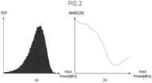
- a PDF may be relatively non-uniform with respect to input power when a modulation signal M_S is used as a training signal, but may be relatively uniform when a multi-tone signal MT_S is used as a training signal. Accordingly, by using a multi-tone signal MT_S having a uniform PDF as a training signal for predistortion, the RF circuit according to example embodiments may prevent degradation of predistortion performance.
- the representative value selection method may be a moving average method for selecting an average value of an output included in each of the plurality of sections as a representative value of each of the plurality of sections.
- the moving average method may be performed based on Equation 3 below.
- f ⁇ x 1 M ⁇ i : x i ⁇ x ⁇ L 2 , x + L 2 y i
- f ⁇ ( x ) is a representative value of a section
- L is a range of the section
- i is an index of a power amplifier model input included in the section
- x i is an i-th input value of the power amplifier model
- y i is an output value of the power amplifier model corresponding to x i
- M is the number of x i included in the section.
- the power amplifier model based on curve fitting may also be inaccurate, which may result in the degradation of predistortion performance.
- the EVM is lower in a high-power section, compared to the modulation signal M_S, when a multi-tone signal MT_S is used. This is because the multi-tone signal MT_S has a uniform PDF, which can secure sufficient samples even in the high-power section.
- an RF circuit 100A may include a phase determination circuit 160, in addition to a multi-tone generation circuit 110, a multiplexer 120, a predistortion circuit 130, a power amplifier 140, and a predistortion modeling circuit 150.
- the phase determination circuit 160 may be configured to determine a phase value of each of a plurality of tones in a multi-tone signal MT_S generated from multi-tone generation circuit 110 (or the multi-tone generation circuit 153 of FIG. 4 ).
- the phase value may be ⁇ k of Equation 1 or Equation 2.
- the phase determination circuit 160 may adjust the phase values of each of the plurality of tones such that the multi-tone signal MT_S has a uniform PDF.
- the multiplexer 120 may select the multi-tone signal MT_S as a training signal and transmit the selected multi-tone signal MT_S to the predistortion circuit 130.
- the predistortion circuit 130 may generate a predistortion signal PD_S based on an updated predistortion model PD_M from the predistortion modeling.
- the power amplifier 140 may amplify the predistorted signal PD_S, and may output an output signal OUT.
- the adjusted phase set may include a first set including the adjusted ⁇ 1 and maintained ⁇ 2 to ⁇ N and a second set including the adjusted ⁇ 2 and maintained ⁇ 1 and ⁇ 3 to ⁇ N .
- the adjusted phase set may include all sets including the adjusted ⁇ k and the remaining preserved phases.
- a plurality of PAPR adjustment values may be a set of PAPRs calculated from each of the different sets included in the adjustment phase set (for example, the set may include PAPRs calculated from the above-mentioned first set and PAPRs calculated from the above-mentioned second set).
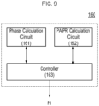
- the PAPR calculation circuit 162 may calculate the PAPR of the multi-tone signal MT_S corresponding to the plurality of phase initial values as a PAPR initial value. As at least one of the plurality of phase initial values is adjusted, the PAPR calculation circuit 162 may calculate the PAPR of the multi-tone signal MT_S corresponding to the adjustment phase set as a plurality of PAPR adjustment values.
- the PAPR may be a ratio of a peak value of power to an average value of the power.
- the controller 163 may be connected to the phase calculation circuit 161 and the PAPR calculation circuit 162, and may determine a phase value of the multi-tone signal MT_S based on the phase initial value and the PAPR.
- the controller 163 may set a minimum value of the at least PAPR initial value as a PAPR initial value. After setting the minimum value as the PAPR initial value, the controller 163 may determine a phase value based on a reset PAPR initial value.
- the controller 163 may transmit phase information PI including the ultimately determined phase value.
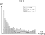
- exemplary training signals are all multi-tone signals (MT_S), and three cases may be provided as follows: a case in which phases of tones are all zero (In-Phase), a case in which phases of tones are randomly different from each other (Out of Phase), and a case in which phases of tones are appropriately determined according to example embodiments (Custom Phase).
- the RF circuit 100 or 100A may amplify the predistortion signal PD_S to output an output signal OUT.
- the output signal OUT, output in operation S130, may be used in operation S140 to model the predistortion model PD_M.
- operations S120 to S140 may be repeated until a requirement for compensation of the nonlinearity of the output signal OUT is satisfied to the maximum extent.
- the multi-tone signal MT_S used as the training signal has a uniform PDF, so that the degradation of predistortion performance may be prevented.
- the RF circuit 100 or 100A may model a power amplifier model, which is a relationship between a predistorted signal PD_S and an output signal OUT corresponding to a multi-tone signal MT_S, based on a moving average method.
- a moving average method requiring a uniform PDF in the curve fitting for modeling the power amplifier model may be adopted.
- the power amplifier model may be modeled without a burden of having to perform certain operations (for example, operations for determining a high-order polynomial in polynomial fitting).
- FIG. 13 is a flowchart illustrating a method of determining a phase of an RF circuit according to example embodiments.
- the RF circuit 100A may determine the phase initial value as a phase value.
- the RF circuit 100A may repeat operations S330 to S360 on the reset PAPR initial value. For example, the RF circuit 100A may determine the phase value by repeating the operations of comparing the reset PAPR initial value of PAPR with the threshold, determining the phase value, calculating the PAPR for the adjustment phase set, and comparing the PAPR initial value with the adjustment phase set.
- the training information determination circuit 200 may determine the training information TI based on at least one of 1) whether a predistortion model PD_M reflecting a memory effect has been used (for example, a memory predistortion model or a memoryless predistortion model), 2) the number of samples of the training signal, and/or a sampling rate of the samples, and 3) a bandwidth of a signal to which the predistortion is to be ultimately applied.
- a predistortion model PD_M reflecting a memory effect for example, a memory predistortion model or a memoryless predistortion model
- the training information determination circuit 200 may determine that a bandwidth, lower than the bandwidth of the modulation signal M_S, is a bandwidth of the multi-tone signal MT_S.
- a memoryless predistortion model may be a model that averages performance characteristics based on frequency. In this case, it may be determined, depending on the frequency characteristics of the power amplifier 140, which of averaging the frequency characteristics of a training signal having a lower bandwidth and averaging the frequency characteristics of a training signal having a wider bandwidth is better in terms of predistortion performance.
- the wider the bandwidth of the training signal the more memory effects may be reflected.
- the need to widen the bandwidth in the memoryless predistortion model, where memory effects are not considered, may be reduced.
- the training information determination circuit 200 may determine the bandwidth of the multi-tone signal MT_S to be lower than the bandwidth of the modulation signal M_S, when the predistortion model PD_M is memoryless.
- the multi-tone generation circuit 110 may also generate a multi-tone signal MT_S having a lower bandwidth.
- the training information determination circuit 200 may also determine whether to decrease the bandwidth, by considering the number of available samples.
- the training information determination circuit 200 may increase the bandwidth to reflect the memory effects more.
- the predistortion model PD_M may reflect the memory effects more.
- the training information determination circuit 200 may increase the number of tones.
- the training information determination circuit 200 may decrease the number of tones to save resources for generating a training signal. However, when the number of tones is significantly decreased, performance degradation may be more likely to occur when the predistortion is applied to the modulation signal M_S having a higher bandwidth than the multi-tone signal MT_S due to the smaller number of samples. Accordingly, the training information determination circuit 200 may determine the number of tones of the multi-tone signal MT_S to be larger than the required number of tones.
- a wireless communication device 300 may include a modem 310, a radio-frequency integrated circuit (RFIC) 320, a power amplifier 330, a duplexer 340, and an antenna 350.
- RFIC radio-frequency integrated circuit
- the multi-tone generation circuit 312 may generate a multi-tone signal to be used as a training signal for the predistortion circuit 313 according to the above-described example embodiments.
- the RFIC 320 may perform a frequency up-conversion on the transmit signal TX to generate an RF input signal RF_IN, or may perform a frequency down-conversion on the RF receive signal RF_R to generate a receive signal RX.
- the RFIC 320 may include a transmit circuit TXC, a receive circuit RXC, and a local oscillator LO.
- the baseband filter ABF1 may filter and provide the transmit signal TX, received from the modem 310, to the first mixer MX1. Then, the first mixer MX1 may perform a frequency up-conversion to convert a frequency of the transmit signal TX from a baseband to a high-frequency band through a frequency signal provided by the local oscillator LO. Through the frequency up-conversion, the transmit signal TX may be provided to the driver amplifier 321 as an RF input signal RF_IN, and the driver amplifier 321 may firstly amplify and provide the RF input signal RF_IN to the power amplifier 330.
- the power amplifier 330 may receive a DC voltage or a variable power supply voltage (for example, a dynamically variable output voltage), and may secondly amplify power of the RF input signal RF_IN based on the received power supply voltage to generate an RF output signal RF_OUT. In this case, the nonlinearity of the RF output signal RF_OUT may be compensated for by the predistortion circuit 313.
- a DC voltage or a variable power supply voltage for example, a dynamically variable output voltage
- the receive circuit RXC may include a second analog baseband filter ABF2, a second mixer MX2, and a low-noise Amplifier (LNA) 322.
- the second analog baseband filter ABF2 may include a low-pass filter.
- the wireless communication device 300 may transmit a transmit signal (e.g., TX) through a plurality of frequency bands using carrier aggregation (CA).
- a transmit signal e.g., TX
- CA carrier aggregation
- the wireless communication device 300 may include a plurality of power amplifiers 330 for amplifying a plurality of RF input signals RF_IN, respectively corresponding to a plurality of carriers.
- the power amplifier 330 is provided in singular.
- the duplexer 340 may be connected to the antenna 350 to separate a transmit frequency and a receive frequency.
- the duplexer 340 may separate an RF output signal RF_OUT, provided by the power amplifier 330, for each frequency band and provide the separated signal to the corresponding antenna 350.
- the duplexer 340 may provide an external signal, received from the antenna 350, to the LNA 322 of the receive circuit RXC of the RFIC 320.
- the duplexer 340 may include a front end module with an integrated duplexer (FEMiD).
- the antenna 350 may transmit an RF output signal RF_OUT, frequency-separated by the duplexer 340, to an external entity or provide the RF receive signal RF_R, received from an external entity, to the duplexer 340.
- the antenna 350 may include an array antenna, but example embodiments are not limited thereto.
- each of the modem 310, the RFIC 320, the power amplifier 330, and the duplexer 340 may be implemented as an integrated circuit (IC), a chip, or a module.
- the modem 310, the RFIC 320, the power amplifier 330, and the duplexer 340 may be mounted together on a printed circuit board (PCB), but example embodiments are not limited thereto.
- PCB printed circuit board
- at least a portion of the modem 310, the RFIC 320, the power amplifier 330, and the duplexer 340 may be implemented as a single communication chip.
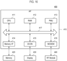
- the CPU 411 may control the modem 416 and/or the RF module 440 to model a power amplifier model, which is a relationship between the predistortion signal and the output signal OUT corresponding to the multi-tone signal, based on a moving average method and to model a predistortion model to compensate for the nonlinearity of the power amplifier model.
- a power amplifier model which is a relationship between the predistortion signal and the output signal OUT corresponding to the multi-tone signal, based on a moving average method and to model a predistortion model to compensate for the nonlinearity of the power amplifier model.
- the CPU 411 may control the modem 416 and/or the RF module 440 to calculate a plurality of phase initial values for the plurality of tones, calculate a PAPR initial value of the multi-tone signal corresponding to the plurality of initial phase values, and determine the phase initial value as a phase value of each of the plurality of tones based on the initial PAPR value being less than a threshold.
- the RAM 412 may temporarily store programs, data, or at least one instruction. For example, programs and/or data stored in memory 420 may be temporarily stored in the RAM 412 under the control of the CPU 411 or a booting code.
- the RAM 412 may be implemented as a DRAM or an SRAM.
- the PMU 413 may manage power of each component of the AP 410.
- the PMU 413 may determine an operating status of each component of the AP 410 and control an operation thereof.
- the memory interface 414 may control the overall operation of the memory 420, and may control data exchange between the memory 420 and each component of the AP 410.
- the memory interface 414 may write data in the memory 420 or read data from the memory 420 according to a request of the CPU 411.
- the memory 420 may store various types of information (for example, a multi-tone signal, training information, or the like) according to the above-described embodiments.
- the memory 420 may store a power amplifier model and a predistortion model as set forth in the above-described embodiments.
- the modem 416 may modulate data to be transmitted appropriately for a wireless environment and recover received data.
- the modem 416 may perform digital communication with the RF module 440.
- the modem 416 may be implemented with modem 310 described above with reference to FIG. 15 .
- the RF module 440 may convert a high-frequency signal, received through an antenna, into a low-frequency signal and transmit the converted low-frequency signal to the modem 416.
- the RF module 440 may convert a low-frequency signal, received from the modem 416, into a high-frequency signal and transmit the converted high-frequency signal to the outside of the electronic device 400 through the antenna.
- the RF module 440 may amplify or filter a signal.
- the modem 416 and the RF module 440 may be implemented with at least one of the RF circuit 100 or 100A, the phase determination circuit 160, and the training information determination circuit 200 according to example embodiments.
- an RF circuit for predistortion and a method of operating the same may be provided.
Landscapes
- Engineering & Computer Science (AREA)
- Power Engineering (AREA)
- Computer Networks & Wireless Communication (AREA)
- Signal Processing (AREA)
- Physics & Mathematics (AREA)
- Nonlinear Science (AREA)
- Microelectronics & Electronic Packaging (AREA)
- Amplifiers (AREA)
Applications Claiming Priority (1)
| Application Number | Priority Date | Filing Date | Title |
|---|---|---|---|
| KR1020230136167A KR20250052857A (ko) | 2023-10-12 | 2023-10-12 | 전치 왜곡을 위한 rf 회로 및 그 동작 방법 |
Publications (2)
| Publication Number | Publication Date |
|---|---|
| EP4539337A2 true EP4539337A2 (de) | 2025-04-16 |
| EP4539337A3 EP4539337A3 (de) | 2025-06-04 |
Family
ID=93037249
Family Applications (1)
| Application Number | Title | Priority Date | Filing Date |
|---|---|---|---|
| EP24205297.5A Pending EP4539337A3 (de) | 2023-10-12 | 2024-10-08 | Hf-schaltung zur vorverzerrung und verfahren zum betrieb davon |
Country Status (4)
| Country | Link |
|---|---|
| US (1) | US20250125825A1 (de) |
| EP (1) | EP4539337A3 (de) |
| KR (1) | KR20250052857A (de) |
| CN (1) | CN119834823A (de) |
Families Citing this family (1)
| Publication number | Priority date | Publication date | Assignee | Title |
|---|---|---|---|---|
| CN120415970B (zh) * | 2025-06-26 | 2025-11-25 | 北京兆维电子(集团)有限责任公司 | 一种信号预失真处理方法、装置、电子设备及存储介质 |
Family Cites Families (3)
| Publication number | Priority date | Publication date | Assignee | Title |
|---|---|---|---|---|
| FR2773423B1 (fr) * | 1998-01-06 | 2001-10-19 | Alsthom Cge Alkatel | Procede et systeme de linearisation numerique d'un amplificateur |
| CN101662435A (zh) * | 2009-09-24 | 2010-03-03 | 中兴通讯股份有限公司 | 数字预失真参数的获取、调整装置及方法 |
| CN103248597B (zh) * | 2013-05-17 | 2017-02-22 | 上海无线通信研究中心 | 基于参考信号的自适应数字预失真系统及初始化校正方法 |
-
2023
- 2023-10-12 KR KR1020230136167A patent/KR20250052857A/ko active Pending
-
2024
- 2024-06-14 US US18/743,260 patent/US20250125825A1/en active Pending
- 2024-10-08 EP EP24205297.5A patent/EP4539337A3/de active Pending
- 2024-10-10 CN CN202411407603.3A patent/CN119834823A/zh active Pending
Also Published As
| Publication number | Publication date |
|---|---|
| US20250125825A1 (en) | 2025-04-17 |
| KR20250052857A (ko) | 2025-04-21 |
| CN119834823A (zh) | 2025-04-15 |
| EP4539337A3 (de) | 2025-06-04 |
Similar Documents
| Publication | Publication Date | Title |
|---|---|---|
| US7888997B2 (en) | Systems, methods, and apparatuses for linear envelope elimination and restoration transmitters | |
| US9094004B2 (en) | Transmitter system with digital phase rotator used for applying digital phase rotation to constellation data and related signal transmission method thereof | |
| US11817892B2 (en) | Digital predistortion of signals | |
| US8030997B2 (en) | Resource efficient adaptive digital pre-distortion system | |
| US7463697B2 (en) | Multicarrier transmitter and methods for generating multicarrier communication signals with power amplifier predistortion and linearization | |
| CN101090380B (zh) | 用于线性包络消除与恢复发射机的系统以及方法 | |
| EP4539337A2 (de) | Hf-schaltung zur vorverzerrung und verfahren zum betrieb davon | |
| CN113285727B (zh) | 一种无线信号的发射装置及其处理方法 | |
| JPH11154880A (ja) | 信号補正方法及び装置、歪補償装置、歪補償データ作成装置及び送信機 | |
| US12457054B2 (en) | Data modulation method and device, data demodulation method and device, service node, terminal, and medium | |
| O'Droma et al. | Signal modeling classes for linearized OFDM SSPA behavioral analysis | |
| JP2001284976A (ja) | アダプティブプリディストーション歪補償方法及び装置 | |
| Ba | Efficient digital baseband predistortion for modern wireless handsets | |
| US20240364275A1 (en) | Rf circuit supporting predistortion and method of operating the same | |
| Vimal et al. | Crests Factor Reduction's Impact on 5g New Radio Signals | |
| CN121966466A (zh) | 用于功率放大器的数字预失真的设备和方法 | |
| WO2026024960A1 (en) | Optimizing power amplifier energy for enhanced network sustainability |
Legal Events
| Date | Code | Title | Description |
|---|---|---|---|
| PUAI | Public reference made under article 153(3) epc to a published international application that has entered the european phase |
Free format text: ORIGINAL CODE: 0009012 |
|
| STAA | Information on the status of an ep patent application or granted ep patent |
Free format text: STATUS: THE APPLICATION HAS BEEN PUBLISHED |
|
| AK | Designated contracting states |
Kind code of ref document: A2 Designated state(s): AL AT BE BG CH CY CZ DE DK EE ES FI FR GB GR HR HU IE IS IT LI LT LU LV MC ME MK MT NL NO PL PT RO RS SE SI SK SM TR |
|
| PUAL | Search report despatched |
Free format text: ORIGINAL CODE: 0009013 |
|
| AK | Designated contracting states |
Kind code of ref document: A3 Designated state(s): AL AT BE BG CH CY CZ DE DK EE ES FI FR GB GR HR HU IE IS IT LI LT LU LV MC ME MK MT NL NO PL PT RO RS SE SI SK SM TR |
|
| RIC1 | Information provided on ipc code assigned before grant |
Ipc: H03F 3/24 20060101ALI20250501BHEP Ipc: H03F 3/19 20060101ALI20250501BHEP Ipc: H03F 1/32 20060101AFI20250501BHEP |
|
| P01 | Opt-out of the competence of the unified patent court (upc) registered |
Free format text: CASE NUMBER: APP_27592/2025 Effective date: 20250610 |
|
| STAA | Information on the status of an ep patent application or granted ep patent |
Free format text: STATUS: REQUEST FOR EXAMINATION WAS MADE |
|
| 17P | Request for examination filed |
Effective date: 20251126 |