EP4539289A1 - Power output circuit and contactless power supply system - Google Patents
Power output circuit and contactless power supply system Download PDFInfo
- Publication number
- EP4539289A1 EP4539289A1 EP23819562.2A EP23819562A EP4539289A1 EP 4539289 A1 EP4539289 A1 EP 4539289A1 EP 23819562 A EP23819562 A EP 23819562A EP 4539289 A1 EP4539289 A1 EP 4539289A1
- Authority
- EP
- European Patent Office
- Prior art keywords
- power
- filter
- reactor
- capacitor
- circuit
- Prior art date
- Legal status (The legal status is an assumption and is not a legal conclusion. Google has not performed a legal analysis and makes no representation as to the accuracy of the status listed.)
- Pending
Links
Images



Classifications
-
- H—ELECTRICITY
- H02—GENERATION; CONVERSION OR DISTRIBUTION OF ELECTRIC POWER
- H02J—ELECTRIC POWER NETWORKS; CIRCUIT ARRANGEMENTS OR SYSTEMS FOR SUPPLYING OR DISTRIBUTING ELECTRIC POWER; SYSTEMS FOR STORING ELECTRIC ENERGY
- H02J50/00—Circuit arrangements or systems for wireless supply or distribution of electric power
- H02J50/10—Circuit arrangements or systems for wireless supply or distribution of electric power using inductive coupling
- H02J50/12—Circuit arrangements or systems for wireless supply or distribution of electric power using inductive coupling of the resonant type
-
- H—ELECTRICITY
- H02—GENERATION; CONVERSION OR DISTRIBUTION OF ELECTRIC POWER
- H02J—ELECTRIC POWER NETWORKS; CIRCUIT ARRANGEMENTS OR SYSTEMS FOR SUPPLYING OR DISTRIBUTING ELECTRIC POWER; SYSTEMS FOR STORING ELECTRIC ENERGY
- H02J50/00—Circuit arrangements or systems for wireless supply or distribution of electric power
- H02J50/005—Mechanical details of housing or structure aiming to accommodate the power transfer means, e.g. mechanical integration of coils, antennas or transducers into emitting or receiving devices
-
- H—ELECTRICITY
- H02—GENERATION; CONVERSION OR DISTRIBUTION OF ELECTRIC POWER
- H02J—ELECTRIC POWER NETWORKS; CIRCUIT ARRANGEMENTS OR SYSTEMS FOR SUPPLYING OR DISTRIBUTING ELECTRIC POWER; SYSTEMS FOR STORING ELECTRIC ENERGY
- H02J50/00—Circuit arrangements or systems for wireless supply or distribution of electric power
- H02J50/40—Circuit arrangements or systems for wireless supply or distribution of electric power using two or more transmitting or receiving devices
- H02J50/402—Circuit arrangements or systems for wireless supply or distribution of electric power using two or more transmitting or receiving devices the two or more transmitting or the two or more receiving devices being integrated in the same unit, e.g. power mats with several coils or antennas with several sub-antennas
-
- H—ELECTRICITY
- H02—GENERATION; CONVERSION OR DISTRIBUTION OF ELECTRIC POWER
- H02M—APPARATUS FOR CONVERSION BETWEEN AC AND AC, BETWEEN AC AND DC, OR BETWEEN DC AND DC, AND FOR USE WITH MAINS OR SIMILAR POWER SUPPLY SYSTEMS; CONVERSION OF DC OR AC INPUT POWER INTO SURGE OUTPUT POWER; CONTROL OR REGULATION THEREOF
- H02M1/00—Details of apparatus for conversion
- H02M1/12—Arrangements for reducing harmonics from AC input or output
- H02M1/126—Arrangements for reducing harmonics from AC input or output using passive filters
-
- H—ELECTRICITY
- H02—GENERATION; CONVERSION OR DISTRIBUTION OF ELECTRIC POWER
- H02J—ELECTRIC POWER NETWORKS; CIRCUIT ARRANGEMENTS OR SYSTEMS FOR SUPPLYING OR DISTRIBUTING ELECTRIC POWER; SYSTEMS FOR STORING ELECTRIC ENERGY
- H02J3/00—Circuit arrangements for AC mains or AC distribution networks
- H02J3/01—Arrangements for reducing harmonics or ripples
-
- H—ELECTRICITY
- H02—GENERATION; CONVERSION OR DISTRIBUTION OF ELECTRIC POWER
- H02J—ELECTRIC POWER NETWORKS; CIRCUIT ARRANGEMENTS OR SYSTEMS FOR SUPPLYING OR DISTRIBUTING ELECTRIC POWER; SYSTEMS FOR STORING ELECTRIC ENERGY
- H02J50/00—Circuit arrangements or systems for wireless supply or distribution of electric power
- H02J50/70—Circuit arrangements or systems for wireless supply or distribution of electric power involving the reduction of electric, magnetic or electromagnetic leakage fields
Definitions
- the present disclosure relates to a power output circuit and a contactless power supply system.
- a filter circuit is used in a power transmission line to obtain a target frequency component or the like.
- a filter circuit for suppressing harmonic noise is used in a power transmission apparatus that is used for contactless power supply.
- a new power transmission line including a filter circuit being added in parallel to a power transmission line including a filter circuit that is already installed can be considered in order to increase power supplied to a load on the power transmission line that is already installed.
- an output current of the filter circuit may become imbalanced among a plurality of filter circuits and power loss may increase.
- Such issues may also arise not only in cases in which power transmission lines including a power source are connected in parallel, but also in cases in which only filter circuits are connected in parallel.
- the power output circuit includes a plurality of circuit blocks that are provided in power wirings to which power is inputted and connected to each other side by side.
- Each of the plurality of circuit blocks includes at least a filter in a last post-stage.
- Each of the plurality of filters includes a reactor and a capacitor connected to the reactor at a node differing from an output node. Either of the reactor and the capacitor provided in each of the plurality of filters is connected to the power wirings in series so as to connect with the output node.
- a connection line between the reactor and the capacitor in one filter is connected to a connection line between the reactor and the capacitor in the remaining other filter.
- connection lines of the plurality of filters are connected. Therefore, variations in a current value and transient characteristics of an output current of the filters can be suppressed. Consequently, increase in power loss in the reactor and the capacitor due to current imbalance attributed to element characteristics of the reactor and the capacitor can be suppressed.
- a power output circuit OC1 is interposed between an alternating current power supply 22 and a load 70 to which power is supplied from the alternating current power supply 22.
- the power output circuit OC1 includes two circuit blocks 30 that are provided in a first power wiring WP1 and a second power wiring WP2 that serve as power wirings to which alternating current power outputted from the alternating current power supply 22 is inputted, and are connected to each other side by side.
- the two circuit blocks 30 are connected to each other in parallel.
- each circuit block 30 includes a filter 16.
- the filter 16 is a bandpass filter configured by a first reactor L1 and a first capacitor C1 connected in series.
- the filter 16 suppresses passage of noise components and allows passage of signals in a target frequency band.
- the first reactor L1 and the first capacitor C1 are connected to the first power wiring WP1 in series. Specifically, one terminal of the first capacitor C1 is connected to an output node Nout of the power output circuit OC1, and another terminal is connected to one terminal of the first reactor L1 at a node differing from the output node Nout. Another terminal of the first reactor L1 is connected to one terminal of the alternating current power supply 22. A connection line between the first reactor L1 and the first capacitor C1 in one filter 16 is connected to a connection line between the first reactor L1 and the first capacitor C1 in the remaining other filter 16. That is, the connection lines between the first reactor L1 and a second capacitor C2 of the two filters 16 are connected by a wiring W1.
- the inventors have confirmed, through simulation, that the imbalance between the two filters 16 in the output currents of the filters 16 is suppressed by the connection lines between the first reactor L1 and the second capacitor C2 being connected.
- the inventors have confirmed, through simulation, characteristics indicating a relationship between frequency and an amount of attenuation even in cases in which the connection lines between the first reactor L1 and the second capacitor C2 are connected, and have confirmed no reduction in filter performance. Therefore, as a result of the connection lines between the first reactor L1 and the second capacitor C2 being connected, current imbalance between the filters in the output current can be suppressed without reduction in filter performance.
- the power output circuit OC1 includes two filters 16, and the connection lines between the first reactor L1 and the second capacitor C2 of each filter 16 are connected by the wiring W1. Therefore, even in cases in which the element characteristics of the first reactor L1 and the first capacitor C1 vary, variations in the current value and transient characteristics of the output current of each filter 16 can be suppressed. Consequently, increase in loss in the first reactor L1 and the first capacitor C1 due to current imbalance caused by the variations in the element characteristics of the first reactor L1 and the first capacitor C1 can be suppressed.
- a circuit block 230 provided in a power output circuit OC2 according to a present embodiment including an inverter 14 in addition to a filter 216 differs from the first embodiment.
- the filter 16 according to the first embodiment is a bandpass filter
- the filter 216 according to the present embodiment is a combination filter of a bandpass filter and a band elimination filter. Configurations identical to those according to the first embodiment are given the same reference numbers. Detailed descriptions are omitted as appropriate.
- the power output circuit OC2 includes two circuit blocks 230 that are provided in the first power wiring WP1 and the second power wiring WP2 to which alternating current power outputted from a direct current power supply 24 is inputted, and are connected to each other in parallel.
- the circuit block 230 includes the inverter 14 and the filter 216.
- the filter 216 is disposed in a last post-stage of the circuit block 230.
- a post-stage means a downstream side in a direction of a flow of power, in which a power supply such as the alternating current power supply 22 is upstream and a load such as the load 70 to which power is supplied is downstream.
- the pre-stage means the upstream side in the direction of the flow of power.
- the inverter 14 converts direct current power outputted from the direct current power supply 24 to alternating current power.
- the filter 216 suppresses passage of noise components of the inputted alternating current power and allows passage of signals in a target frequency band.
- the filter 216 is configured such that a first filter unit F1 that is a bandpass filter, a second filter unit F2 that is a band elimination filter, and a third filter unit F3 that is a bandpass filter are connected in this order.
- the first filter unit F1 is configured by a connection body in which a first reactor L1 and a first capacitor C1 are connected in series being inserted in the first power wiring WP1 in series.
- the second filter unit F2 is configured by a connection body in which a second reactor L2 and a second capacitor C2 are connected to each other in parallel being connected to the direct current power supply 24 in parallel.
- the third filter unit F3 is configured by a connection body in which a third reactor L3 and a third capacitor C3 are connected in series being inserted in the first power wiring WP1 in series.
- connection lines of the two filters 216 are connected by the wiring W1.
- the connection lines between the third reactor L3 and the third capacitor C3 connected to the output node Nout are connected by the wiring W1. Consequently, in addition to effects similar to those according to the first embodiment being achieved, variations in the current value and transient characteristics of the output current of the filters 216 can be suppressed even in cases in which differences occur in the current value and transient characteristics of the output current of the two inverters 14 provided in the power output circuit OC2.
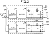
- a circuit block 330 provided in a power output circuit OC3 according to a present embodiment having an alternating current-to-direct current (AC/DC) converter 12 in addition to a filter 316 and the inverter 14 differs from the second embodiment.
- the filter 316 according to the present embodiment being configured as a fourth-order filter differs from the above-described embodiments. Configurations identical to those according to the above-described embodiments are given the same reference numbers. Detailed descriptions are omitted as appropriate.
- the power output circuit OC3 includes two circuit blocks 330 that are provided in the first power wiring WP1 and the second power wiring WP2 to which alternating current power outputted from the alternating current power supply 22 is inputted, and are connected to each other in parallel.
- the circuit block 330 includes the AC/DC converter 12, the inverter 14, and the filter 316.
- the filter 316 is disposed in the last post-stage of the circuit block 330.
- the AC/DC converter 12 converts the alternating current power outputted from the alternating current power supply 22 to a direct current voltage of a target voltage value and supplies the direct current voltage to the inverter 14.
- the filter 316 is configured as a fourth-order filter. Specifically, a connection body in which a first reactor L1 and a second reactor L2 are connected in series is inserted in the first power wiring WP1 in series. A first capacitor C1 is inserted between the first reactor L1 and the second reactor L2 in parallel with the alternating current power supply 22. A second capacitor C2 is inserted following the second reactor L2 in parallel with the alternating current power supply 22.
- the internal connection lines of the two filters 316 are connected by the wiring W1. Specifically, the connection lines between the first capacitor C1 and the second reactor L2 connected to the output node Nout are connected by the wiring W1. Consequently, in addition to effects similar to those according to the above-described embodiments being achieved, variations in the current value and transient characteristics of the output current of the filters 316 can be suppressed even in cases in which differences occur in the current value of the output current of the two AC/DC converters 12 provided in the power output circuit OC2.
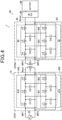
- a power output circuit OC4 and a reception-side power output circuit OCR4 serving as a power output circuit are incorporated in a contactless power supply system 1.
- the contactless power supply system 1 includes a power transmission apparatus 10 and a power reception apparatus 80.
- the power transmission apparatus 10 supplies power to the power reception apparatus 80 without contact.
- the power output circuit OC4 includes two circuit blocks 430 connected to each other in parallel.
- Each circuit block 430 includes a filter 416.
- the filter 416 according to the present embodiment is configured as a fifth-order filter, unlike the above-described embodiments. Configurations identical to those according to the above-described embodiments are given the same reference numbers. Detailed descriptions are omitted as appropriate
- the filter 416 attenuates a harmonic component that is a noise component of high-frequency power that is high-frequency alternating current power inputted from the alternating current power supply 22, allows passage of power in a target frequency band, and supplies the power to a power transmission coil Ls.
- high frequency refers to power at a frequency of 1 kHz or higher.
- a connection body in which a first reactor L1, a second reactor L2, and a third reactor L3 are connected in series is inserted in the first power wiring WP1.
- a first capacitor C1 is connected between the first reactor L1 and the second reactor L2 in parallel with the alternating current power supply 22, and a second capacitor C2 is connected between the second reactor L2 and the third reactor L3 in parallel with the alternating current power supply 22.
- the power transmission coil Ls is connected in the post-stage of the circuit block 430.
- the power reception apparatus 80 includes a power reception coil Lr, the reception-side power output circuit OCR4, a rectifier circuit 86, and a battery 88.
- the power reception coil Lr When the power reception coil Lr is disposed in a position enabling magnetic coupling with the power transmission coil Ls, electromotive force is generated in the power reception coil Lr as a result of electromagnetic induction due to magnetic flux generated by the power transmission coil Ls.
- the electromotive force generated in the power reception coil Lr is inputted to the first power wiring WPr1 and the second power wiring WPr2 serving as power wirings.
- the reception-side power output circuit OCR4 is disposed in a first power wiring WPr1 and a second power wiring WPr2.
- the reception-side power output circuit OCR4 includes two circuit blocks 84 connected to each other in parallel.
- Each circuit block 84 includes a filter 90.
- the filter 90 is configured as a fifth-order filter that includes a fourth reactor L4, a fifth reactor L5, a sixth reactor L6, a third capacitor C3, and a fourth capacitor C4.
- the filter 90 attenuates a harmonic component of alternating current power inputted from the power reception coil Lr.
- the rectifier circuit 86 converts the inputted alternating current power to direct current power and supplies the direct current power to the battery 88.
- the power transmission coil Ls and the power reception apparatus 80 can be considered to be loads
- the internal connection lines of the two filters 416 are connected by the wiring W1 and the wiring W2.
- the connection lines between the second capacitor C2 and the third reactor L3 connected to the output node Nout are connected by the wiring W2.
- the connection lines between the second reactor L2 and the first capacitor C1 are connected by the wiring W1. Consequently, variations in the current value and transient characteristics of the output current of the filters 416 can be suppressed even in cases in which variations occur in the inductance of the reactors and the capacitance of the capacitors.
- connection lines of the two filters 90 provided in the power reception apparatus 80 are connected by a wiring W3 and a wiring W4.
- the connection lines between the fourth capacitor C4 and the sixth reactor L6 connected to the output node Nout of the reception-side power output circuit OCR4 are connected by the wiring W4.
- the connection lines between the third capacitor C3 and the fifth reactor L5 are connected by the wiring W3. Consequently, in a manner similar to the power output circuit OC4, variations in the current value and transient characteristics of the output current of the filters 90 can be suppressed even in cases in which variations occur in the inductance of the reactors and the capacitance of the capacitors.
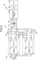
- a present embodiment is identical to the fourth embodiment in that a power output circuit OC5 and a reception-side power output circuit OCR5 are incorporated in a contactless power supply system 501.
- the present embodiment differs from the fourth embodiment in terms of a circuit block 530 according to the present embodiment having the inverter 14, a transmission resonance circuit 18 being provided, and a circuit configuration of a filter 516.
- a power reception apparatus 580 according to the present embodiment differs from the fourth embodiment in terms of having a reception resonance circuit 82. Configurations identical to those according to the above-described embodiments are given the same reference numbers. Detailed descriptions are omitted as appropriate
- the circuit block 530 includes the inverter 14 in a manner similar to the second embodiment.
- the filter 516 is a combination filter of a bandpass filter and a band elimination filter. Specifically, the filter 516 is configured such that a first filter unit F1 that is a bandpass filter and a second filter unit F2 that is a band elimination filter are connected in this order.
- the transmission resonance circuit 18 is a resonance circuit in which a transmission resonance capacitor Cs and the power transmission coil Ls are connected in series.
- the transmission resonance circuit 18 enters a resonant state at a fundamental frequency of the alternating current power outputted from the inverter 14.
- the fundamental frequency is 85 kHz.
- the reception resonance circuit 82 is a resonance circuit in which the power reception coil Lr and a reception resonance capacitor Cr are connected in series.
- a resonance frequency of the transmission resonance circuit 18 and a resonance frequency of the reception resonance circuit 82 are set to be substantially the same. Consequently, contactless power supply from the power transmission apparatus 510 to the power reception apparatus 580 can be performed by magnetic resonance between the power transmission coil Ls and the power reception coil Lr.
- the power reception apparatus 580 is mounted in a vehicle (not shown).
- the battery 88 is a secondary battery that outputs direct current power to drive a driving motor that is a driving source of the vehicle.
- the transmission resonance circuit 18 provided in the power transmission device 10 is set in a road on which the vehicle travels.
- connection lines of the two filters 516 are connected by the wiring W1. Specifically, the connection lines between a first reactor L1 and a first capacitor C1 connected to the output node Nout are connected by the wiring W1.
- each circuit block 530 is unitized. Specifically, in the circuit block 530, electronic elements configuring the inverter 14 and the filter 516 are fixed to a substrate, and external connection terminals T1 to T5 are provided on the substrate.
- the external connection terminal T1 and the external connection terminal T3 are provided in the first power wiring WP1.
- the external connection terminal T2 and the external connection terminal T4 are provided in the second power wiring WP2.
- the external connection terminal T1 and the external connection terminal T2 are input-side terminals of the circuit block 530, and the external connection terminal T3 and external connection terminal T4 are output-side terminals of the circuit block 530.
- the external connection terminal T5 is provided in the wiring W1.
- the direct current power supply 24, the unitized circuit block 530, and the transmission resonance circuit 18 are individually disposed.
- the direct current power supply 24 and the circuit block 530, and the circuit block 530 and the transmission resonance circuit 18 are each connected by power wirings.
- the circuit block 530 may be configured to be disposed inside a housing (not shown), and the external connection terminals T1 to T5 may be exposed from the housing.
- power supply capacity of the power transmission apparatus 510 can be flexibly changed as a result of the circuit block 520 having the inverter 14. Specifically, when power supplied from the power transmission apparatus 510 to the transmission resonance circuit 18 is to be increased, the supply capacity can be increased by a new circuit block 530 being added in parallel to the circuit block 530 that is already set. Conversely, when the power supplied by the power transmission apparatus 510 is to be reduced, the supply capacity can be reduced by a portion of the plurality of circuit blocks 530 that are already set being removed.
- the circuit block 530 is unitized, the power wirings for input and the power wirings for output of the circuit block 530 can be easily connected or disconnected using the external connection terminals T1 to T5 provided in advance.
- circuit constants of the inverter 14 and the filter 516 provided in the circuit block 530 can be optimized.
- advantages of the circuit block 530 being unitized are not limited to when the power transmission apparatus 510 is set.
- a case in which the power reception apparatus 580 is mounted in a vehicle is given as an example.
- an object in which the power reception apparatus 580 is mounted is not limited to the vehicle and may be other moving bodies such as an autonomous guided vehicle (AGV).
- AGV autonomous guided vehicle
- a magnitude of power supplied without contact by the contactless power supply system 501 varies depending on the object in which the power reception apparatus 580 is mounted.
- the circuit blocks 530 are manufactured to individually accommodate the various magnitudes of power supplied without contact, a large variety of circuit blocks 530 are required to be prepared.
- the various magnitudes of power supplied without contact can be accommodated through increase and decrease of the number of circuit blocks 530, without a large variety of circuit blocks 530 being prepared.
- a circuit configuration of a reception resonance circuit 682 according to the present embodiment differs from the fifth embodiment. Configurations identical to those according to the above-described embodiments are given the same reference numbers. Detailed descriptions are omitted as appropriate
- a circuit block 630 includes the AC/DC converter 12 in a manner similar to the third embodiment.
- a filter 616 is a balanced-type bandpass filter. Specifically, a first connection body in which a first reactor L1 and a first capacitor C1 are connected in series is provided in the first power wiring WP1, and a second connection body that is a connection body similar to the first connection body and in which a second reactor L2 and a second capacitor C2 are connected in series is provided in the second power wiring WP2.
- the balanced type common mode noise can be reduced.
- connection lines of the two filters 616 are connected by the wiring W1 and the wiring W2. Specifically, connection lines between the first reactor L1 and the first capacitor C1 connected to the output node Nout are connected by the wiring W1.
- a connection line between the second reactor L2 of the second connection body provided in the second power wiring WP2 and the first capacitor C1 in one filter 616 is connected to a connection line between the second reactor L2 and the second capacitor C2 of the second connection body provided in the second power wiring WP2 in the remaining other filter 616.
- the connection lines between the second reactor L2 and the second capacitor C2 are connected by the wiring W2.
- the wiring W1 and the wiring W2 are disposed near each other.
- the wiring W1 and the wiring W2 are twisted together.
- the wiring W1 and the wiring W2 form a pair, wiring inductance can be reduced and a potential difference between the connection lines can be further eliminated. Therefore, variations in the current value and transient characteristics of the output current of the filters 616 can be suppressed. Furthermore, because each line includes a balanced configuration, common mode noise can be further reduced.
- the transmission resonance circuit 618 according to the present embodiment being a resonance circuit in which the transmission resonance capacitor Cs and the power transmission coil Ls are connected in parallel differs from the fifth embodiment.
- the reception resonance circuit 682 according to the present embodiment being a resonance circuit in which the reception resonance capacitor Cr and the power reception coil Lr are connected in parallel differs from the fifth embodiment.
- the contactless power supply system 1 is capable of performing contactless power supply by magnetic field resonance between the power transmission coil Ls and the power reception coil Lr in a manner similar to the fifth embodiment by having the transmission resonance circuit 618 and the reception resonance circuit 682.
- the circuit block 630 is unitized.
- the power output circuit OC6 includes the wiring W2 in addition to the wiring W1 and therefore includes an external connection terminal T6 provided in the wiring W2 in addition to the external connection terminals T1 to T5.
- the circuit block 630 is unitized, the power supply capacity of the power transmission apparatus 610 can be flexibly changed.
- circuit constants of the AC/DC converter 12, the inverter 14 and the filter 516 provided in the circuit block 630 can be optimized.
- power supply capacity of the power transmission apparatus 610 can be flexibly changed in a manner similar to that according to the fifth embodiment as a result of the circuit block 630 having the AC/DC converter 12 and the inverter 14. That is, when power supplied from the power transmission apparatus 610 is to be increased, a new circuit block 630 is added. When power supplied from the power transmission apparatus 610 is to be decreased, the circuit block 630 is removed. Supply capacity can thereby by increased and decreased.
- a contactless power supply system 701 differs from the sixth embodiment in terms of a number of circuit blocks 730, a number of transmission resonance circuits 18, and a configuration of a filter 716. Configurations identical to those according to the above-described embodiments are given the same reference numbers. Detailed descriptions are omitted as appropriate.
- a power transmission apparatus 710 includes three circuit blocks 730.
- the filter 716 is a balanced-type filter. Specifically, a first connection body that includes a first reactor L1 and a second reactor L2 connected to each other in series, and a first capacitor C1 connected between the first reactor L1 and the second reactor L2 in parallel with the alternating current power supply 22 is provided in the first power wiring WP1.
- a second connection body that is a connection body equivalent to the first connection body and includes a third reactor L3 and a fourth reactor L4 connected to each other in series, and a first capacitor C1 connected between the third reactor L3 and the fourth reactor L4 in parallel is provided in the second power wiring WP2.
- a second capacitor C2 is connected following the fourth reactor L4 in parallel with the alternating current power supply 22.
- connection lines of the three filters 616 are connected by the wiring W1 and the wiring W2. Specifically, connection lines between the first reactor L1 and the second reactor L2 connected to the output node Nout of the three filters 616 are connected by the wiring W1. Connection lines between the third reactor L3 and the fourth reactor L4 of the three filters 616 are connected by the wiring W2.
- the wiring W1 and the wiring W2 are disposed near each other. As a result, variations in the current value and transient characteristics of the output current of the filters 716 can be suppressed. In addition, because the wiring W1 and the wiring W2 form a pair, common mode noise can be further reduced.
- the power transmission apparatus 710 includes four transmission resonance circuits 18.
- the four transmission resonance circuits 18 are connected to each other in parallel.
- an example is given in which contactless power supply is performed to a plurality of power reception apparatuses 580 using a plurality of transmission resonance circuits 18 to which power is supplied from the same alternating current power supply 22.
- a magnitude of output power of the power output circuit OC7 is greater than that when contactless power supply to a single power reception apparatus 580 is performed.
- the magnitude of output power of the power transmission apparatus 710 can be adjusted by the circuit block 730 being increased. According to the seventh embodiment described above, effects similar to those according to the above-described embodiments are achieved.
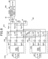
- a power transmission apparatus 810 of a contactless power supply system 801 according to a present embodiment having a three-phase inverter 814 differs from the fifth embodiment. Configurations identical to those according to the above-described embodiments are given the same reference numbers. Detailed descriptions are omitted as appropriate.
- a circuit block 830 provided in a power output circuit OC8 according to the present embodiment includes the three-phase inverter 814.
- the three-phase inverter 814 converts direct current power inputted from the direct current power supply 24 to three-phase alternating current power and outputs the three-phase alternating current power to a third power wiring WP3, a fourth power wiring WP4, and a fifth power wiring WP5 serving as power wirings.
- Two circuit blocks 830 are connected to each other side by side.
- the two circuit blocks 830 being connected side by side also includes, in addition to the case in which the two circuit blocks 830 are connected in parallel as according to the above-described embodiments, a case in which, as according to the present embodiment, a plurality of circuit blocks 830 are connected such that the output nodes Nf of the circuit blocks 830 from which the alternating current power of the same phase is outputted are connected and the alternating current power outputted from the circuit blocks 830 merge.
- a filter 816 is disposed in the third power wiring WP3, the fourth power wiring WP4, and the fifth power wiring WP5. Specifically, a connection body in which a first reactor L1 and a first capacitor C1 are connected in series is inserted in each of the third power wiring WP3, the fourth power wiring WP4, and the fifth power wiring WP5. Power is supplied to the transmission resonance circuit 18 through any two power wirings among the third power wiring WP3, the fourth power wiring WP4, and the fifth power wiring WP5.
- connection lines of the two filters 816 are connected by the wiring W1, the wiring W2, and the wiring W3. Specifically, connection lines between the first reactor L1 and the first capacitor C1 connected to the output node Nout provided in the third power wiring WP3 are connected by the wiring W1. Connection lines between the first reactor L1 and the first capacitor C1 provided in the fourth power wiring WP4 are connected by the wiring W2. Connection lines between the first reactor L1 and the first capacitor C1 provided in the fifth power wiring WP5 are connected by the wiring W3. As a result, variations in the current value and transient characteristics of the output current of the filters 816 can be suppressed. According to the eighth embodiment described above, effects similar to those according to the above-described embodiments are achieved.
- a power transmission apparatus 91 provided in a contactless power supply system 901 according to the present embodiment further having a control circuit 42 serving as a control unit, a current detection circuit 44, and a current sensor 46, and a circuit configuration of a filter 916 differ from the sixth embodiment.
- the control circuit 42 and the current detection circuit 44 are actualized by an electronic circuit. Configurations identical to those according to the first embodiment are given the same reference numbers. Detailed descriptions are omitted as appropriate.
- the filter 916 provided in a circuit block 930 provided in a power output circuit OC9 is a balanced-type filter. Specifically, a first connection body including a first reactor L1, a second reactor L2, and a third reactor L3 that are connected to one another in series, a first capacitor C1 connected between the first reactor L1 and the second reactor L2 in parallel with the alternating current power supply 22, and a second capacitor C2 connected between the second reactor L2 and the third reactor L3 in parallel with the alternating current power supply 22 is provided in the first power wiring WP1.
- a second connection body that is a connection body similar to the first connection body including a fourth reactor L4, a fifth reactor L5, and a sixth reactor L6 that are connected to one another in series, a first capacitor C1 connected between the fourth reactor L4 and the fifth reactor L5 in parallel with the alternating current power supply 22, and a second capacitor C2 connected between the fifth reactor L5 and the sixth reactor L6 in parallel with the alternating current power supply 22 is provided in the second power wiring WP2.
- the balanced type common mode noise can be reduced.
- connection lines of the two filters 916 are connected by the wiring W1, the wiring W2, the wiring W3, and the wiring W4. Specifically, connection lines between the second capacitor C2 and the third reactor L3 connected to the output node Nout are connected by the wiring W1. Connection lines between the sixth reactor L6 and the capacitor C2 are connected by the wiring W2. Connection lines between the first capacitor C1 and the second reactor L2 are connected by the wiring W3. Connection lines between the fifth reactor L5 and the first capacitor C1 are connected by the wiring W4. The wiring W1 and the wiring W2 are disposed near each other. The wiring W3 and the wiring W3 are disposed near each other. As a result, variations in the current value and transient characteristics of the output current of the filters 916 can be suppressed. In addition, common mode noise can be further reduced.
- the control circuit 42 adjusts an input signal to the inverter 14 so that the current difference is reduced using the signal inputted from the current detection circuit 44. Specifically, the control circuit 42 changes the duty of the PWM signal that is an input signal to a transistor configuring the inverter 14. For example, when the output current of one filter 916 is large, the duty of the PWM signal to the inverter 14 inputting power to the one filter 916 may be decreased. As a result, variations in the current value of the output current of the filters 916 can be further suppressed.
- the filter 90 included in the power reception apparatus 80 is a fifth-order filter identical to the filter 416 included in the power transmission apparatus 10.
- the configuration of the filter may differ between the power reception apparatus 80 and the power transmission apparatus 10. Regardless of the configuration of the filter, as a result of the power transmission apparatus 10 and the power reception apparatus 10 including the filters, noise components can be appropriately attenuated.
- the filter 416 is provided in the pre-stage of the power transmission coil Ls of the power transmission apparatus 10 and the filter 90 is provided in the post-stage of the power reception coil Lr of the power reception apparatus 80.
- the filter 416 is provided in the pre-stage of the power transmission coil Ls of the power transmission apparatus 10 and the filter 90 is provided in the post-stage of the power reception coil Lr of the power reception apparatus 80.
- an aspect in which a filter is provided in only either of the pre-stage of the power transmission coil Ls and the post-stage of the power reception coil Lr is also possible.
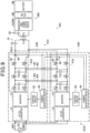
- a power output circuit including: a plurality of circuit blocks (30, 230 to 930) provided in power wirings (WP1 to WP5, WPr1, WPr2) to which power is inputted and connected to each other side by side, in which: each of the plurality of circuit blocks includes at least a filter (16, 90, 216 to 916) in a last post-stage; each of the plurality of filters includes a reactor (L1) and a capacitor (C1) connected to the reactor at a node differing from an output node (Nout); either of the reactor and the capacitor provided in each of the plurality of filters is connected to the power wirings in series so as to connect with the output node; and a connection line between the reactor and the capacitor in one filter is connected to a connection line between the reactor and the capacitor in the remaining other filter.
- the power transmission apparatus further includes a transmission resonance capacitor (Cs) that forms a transmission resonance circuit with the power transmission coil; and the power reception apparatus further includes a reception resonance capacitor (Cr) that forms a reception resonance circuit with the power reception coil.
- Cs transmission resonance capacitor
- Cr reception resonance capacitor
- the power output circuit according to the first aspect in which the filter is a bandpass filter.
- the power output circuit in which the filter is a combination filter of a bandpass filter and a band elimination filter.
- the power output circuit according to the first aspect in which the filter is a fourth-order filter.
- the power output circuit according to the first aspect in which the filter is a fifth-order filter.
- the power wirings include a first power wiring (WP1) and a second power wiring (WP2); a first connection body including the reactor and the capacitor is provided in the first power wiring; the filter is a balanced-type filter having a second connection body equivalent to the first connection body in the second power wiring; and a connection line between the reactor and the capacitor of the second connection body provided in the second power wiring in one filter is connected to a connection line between the reactor and the capacitor of the second connection body provided in the second power wiring in the remaining other filter.
- WP1 first power wiring
- WP2 second power wiring
- the power transmission apparatus further includes an alternating current-to-direct current converter (12) that converts alternating current power to direct current power and outputs the direct current power;
- the power output circuit is provided in a pre-stage of the power transmission coil that is a post-stage of the alternating current-to-direct current converter;
- each of the plurality of circuit blocks includes an inverter (14) that converts the direct current power to the high-frequency power and outputs the high-frequency power to the filter; and each of the plurality of circuit blocks is unitized.
- each of the plurality of circuit blocks includes an alternating current-to-direct current converter (12) that converts alternating current power to direct current power and outputs the direct current power and an inverter (14) that converts the direct current power to the high-frequency power and outputs the high-frequency power to the filter; and each of the plurality of circuit blocks is unitized.
- the power transmission apparatus further includes: a plurality of current sensors (46) that detect an output current of each of the plurality of filters; and a control unit (42) that controls a duty of a pulse width modulation signal for controlling the inverter so that a difference between the output current of one filter and the output current of the remaining other filter is reduced, using a plurality of output currents detected by the plurality of current sensors.
Landscapes
- Engineering & Computer Science (AREA)
- Power Engineering (AREA)
- Computer Networks & Wireless Communication (AREA)
- Physics & Mathematics (AREA)
- Electromagnetism (AREA)
- Inverter Devices (AREA)
Abstract
Description
- The present application is based on and claims the benefit of priority from
Japanese Patent Application No. 2022-92228, filed on June 7, 2022 - The present disclosure relates to a power output circuit and a contactless power supply system.
- Conventionally, a filter circuit is used in a power transmission line to obtain a target frequency component or the like. For example, in
PTL 1, a filter circuit for suppressing harmonic noise is used in a power transmission apparatus that is used for contactless power supply. - [PTL 1]
JP 2016-025771 A - Incidentally, a new power transmission line including a filter circuit being added in parallel to a power transmission line including a filter circuit that is already installed can be considered in order to increase power supplied to a load on the power transmission line that is already installed. In this case, when variations occur in element characteristics such as inductance and capacitance of electronic elements such as reactors and capacitors used in the filter circuits, an output current of the filter circuit may become imbalanced among a plurality of filter circuits and power loss may increase. Such issues may also arise not only in cases in which power transmission lines including a power source are connected in parallel, but also in cases in which only filter circuits are connected in parallel.
- The present disclosure can be implemented according to the following aspects.
- An aspect of the present disclosure provides a power output circuit. The power output circuit includes a plurality of circuit blocks that are provided in power wirings to which power is inputted and connected to each other side by side. Each of the plurality of circuit blocks includes at least a filter in a last post-stage. Each of the plurality of filters includes a reactor and a capacitor connected to the reactor at a node differing from an output node. Either of the reactor and the capacitor provided in each of the plurality of filters is connected to the power wirings in series so as to connect with the output node. A connection line between the reactor and the capacitor in one filter is connected to a connection line between the reactor and the capacitor in the remaining other filter.
- As a result of the power output circuit according to this aspect, connection lines of the plurality of filters are connected. Therefore, variations in a current value and transient characteristics of an output current of the filters can be suppressed. Consequently, increase in power loss in the reactor and the capacitor due to current imbalance attributed to element characteristics of the reactor and the capacitor can be suppressed.
- The above-described object, other objects, characteristics, and advantages of the present disclosure will be further clarified through the detailed description herebelow, with reference to the accompanying drawings. The drawings are as follows:
-
Fig. 1 is a circuit diagram of a power output circuit according to a first embodiment; -
Fig. 2 is a circuit diagram of a power output circuit according to a second embodiment; -
Fig. 3 is a circuit diagram of a power output circuit according to a third embodiment; -
Fig. 4 is a circuit diagram of a contactless power supply system according to a fourth embodiment; -
Fig. 5 is a circuit diagram of a contactless power supply system according to a fifth embodiment; -
Fig. 6 is a circuit diagram of a contactless power supply system according to a sixth embodiment; -
Fig. 7 is a circuit diagram of a contactless power supply system according to a seventh embodiment; -
Fig. 8 is a circuit diagram of a contactless power supply system according to an eighth embodiment; and -
Fig. 9 is a circuit diagram of a contactless power supply system according to a ninth embodiment. - As shown in
Fig. 1 , a power output circuit OC1 is interposed between an alternatingcurrent power supply 22 and aload 70 to which power is supplied from the alternatingcurrent power supply 22. Specifically, the power output circuit OC1 includes twocircuit blocks 30 that are provided in a first power wiring WP1 and a second power wiring WP2 that serve as power wirings to which alternating current power outputted from the alternatingcurrent power supply 22 is inputted, and are connected to each other side by side. Specifically, the twocircuit blocks 30 are connected to each other in parallel. According to the present embodiment, eachcircuit block 30 includes afilter 16. - According to the present embodiment, the
filter 16 is a bandpass filter configured by a first reactor L1 and a first capacitor C1 connected in series. Thefilter 16 suppresses passage of noise components and allows passage of signals in a target frequency band. - The first reactor L1 and the first capacitor C1 are connected to the first power wiring WP1 in series. Specifically, one terminal of the first capacitor C1 is connected to an output node Nout of the power output circuit OC1, and another terminal is connected to one terminal of the first reactor L1 at a node differing from the output node Nout. Another terminal of the first reactor L1 is connected to one terminal of the alternating
current power supply 22. A connection line between the first reactor L1 and the first capacitor C1 in onefilter 16 is connected to a connection line between the first reactor L1 and the first capacitor C1 in the remainingother filter 16. That is, the connection lines between the first reactor L1 and a second capacitor C2 of the twofilters 16 are connected by a wiring W1. As a result, a potential difference between the connection lines can be eliminated. Therefore, even in cases in which variations occur in the inductance of the first reactor L1 and the capacitance of the first capacitor C1, variations in a current value and transient characteristics of an output current that is a current of an output node Nf of eachfilter 16 can be suppressed. Consequently, increase in loss in the first reactor L1 and the first capacitor C1 due to current imbalance caused by variations in the element characteristics of the first reactor L1 and the first capacitor C1, specifically, inductance and capacitance of the first reactor L1 and the first capacitor C1, can be suppressed. - Here, the inventors have confirmed, through simulation, that the imbalance between the two
filters 16 in the output currents of thefilters 16 is suppressed by the connection lines between the first reactor L1 and the second capacitor C2 being connected. In addition, the inventors have confirmed, through simulation, characteristics indicating a relationship between frequency and an amount of attenuation even in cases in which the connection lines between the first reactor L1 and the second capacitor C2 are connected, and have confirmed no reduction in filter performance. Therefore, as a result of the connection lines between the first reactor L1 and the second capacitor C2 being connected, current imbalance between the filters in the output current can be suppressed without reduction in filter performance. - According to the first embodiment described above, the power output circuit OC1 includes two
filters 16, and the connection lines between the first reactor L1 and the second capacitor C2 of eachfilter 16 are connected by the wiring W1. Therefore, even in cases in which the element characteristics of the first reactor L1 and the first capacitor C1 vary, variations in the current value and transient characteristics of the output current of eachfilter 16 can be suppressed. Consequently, increase in loss in the first reactor L1 and the first capacitor C1 due to current imbalance caused by the variations in the element characteristics of the first reactor L1 and the first capacitor C1 can be suppressed. - As shown in
Fig. 2 , acircuit block 230 provided in a power output circuit OC2 according to a present embodiment including aninverter 14 in addition to afilter 216 differs from the first embodiment. In addition, whereas thefilter 16 according to the first embodiment is a bandpass filter, thefilter 216 according to the present embodiment is a combination filter of a bandpass filter and a band elimination filter. Configurations identical to those according to the first embodiment are given the same reference numbers. Detailed descriptions are omitted as appropriate. - The power output circuit OC2 according to the present embodiment includes two
circuit blocks 230 that are provided in the first power wiring WP1 and the second power wiring WP2 to which alternating current power outputted from a directcurrent power supply 24 is inputted, and are connected to each other in parallel. According to the present embodiment, thecircuit block 230 includes theinverter 14 and thefilter 216. Thefilter 216 is disposed in a last post-stage of thecircuit block 230. Here, a post-stage means a downstream side in a direction of a flow of power, in which a power supply such as the alternatingcurrent power supply 22 is upstream and a load such as theload 70 to which power is supplied is downstream. This similarly applies to a pre-stage described hereafter. That is, the pre-stage means the upstream side in the direction of the flow of power. - The
inverter 14 converts direct current power outputted from the directcurrent power supply 24 to alternating current power. Thefilter 216 suppresses passage of noise components of the inputted alternating current power and allows passage of signals in a target frequency band. Thefilter 216 is configured such that a first filter unit F1 that is a bandpass filter, a second filter unit F2 that is a band elimination filter, and a third filter unit F3 that is a bandpass filter are connected in this order. The first filter unit F1 is configured by a connection body in which a first reactor L1 and a first capacitor C1 are connected in series being inserted in the first power wiring WP1 in series. The second filter unit F2 is configured by a connection body in which a second reactor L2 and a second capacitor C2 are connected to each other in parallel being connected to the directcurrent power supply 24 in parallel. The third filter unit F3 is configured by a connection body in which a third reactor L3 and a third capacitor C3 are connected in series being inserted in the first power wiring WP1 in series. - According to the present embodiment as well, internal connection lines of the two
filters 216 are connected by the wiring W1. Specifically, the connection lines between the third reactor L3 and the third capacitor C3 connected to the output node Nout are connected by the wiring W1. Consequently, in addition to effects similar to those according to the first embodiment being achieved, variations in the current value and transient characteristics of the output current of thefilters 216 can be suppressed even in cases in which differences occur in the current value and transient characteristics of the output current of the twoinverters 14 provided in the power output circuit OC2. - According to the second embodiment described above, effects similar to those according to the above-described embodiment are achieved. Furthermore, variations in the current value and transient characteristics of the output current of the
filters 216 can be suppressed even in cases in which differences occur in the current value and transient characteristics of the output current of the twoinverters 14 provided in the power output circuit OC2. - As shown in
Fig. 3 , acircuit block 330 provided in a power output circuit OC3 according to a present embodiment having an alternating current-to-direct current (AC/DC)converter 12 in addition to afilter 316 and theinverter 14 differs from the second embodiment. In addition, thefilter 316 according to the present embodiment being configured as a fourth-order filter differs from the above-described embodiments. Configurations identical to those according to the above-described embodiments are given the same reference numbers. Detailed descriptions are omitted as appropriate. - The power output circuit OC3 according to the present embodiment includes two
circuit blocks 330 that are provided in the first power wiring WP1 and the second power wiring WP2 to which alternating current power outputted from the alternatingcurrent power supply 22 is inputted, and are connected to each other in parallel. According to the present embodiment, thecircuit block 330 includes the AC/DC converter 12, theinverter 14, and thefilter 316. Thefilter 316 is disposed in the last post-stage of thecircuit block 330. - The AC/
DC converter 12 converts the alternating current power outputted from the alternatingcurrent power supply 22 to a direct current voltage of a target voltage value and supplies the direct current voltage to theinverter 14. Thefilter 316 is configured as a fourth-order filter. Specifically, a connection body in which a first reactor L1 and a second reactor L2 are connected in series is inserted in the first power wiring WP1 in series. A first capacitor C1 is inserted between the first reactor L1 and the second reactor L2 in parallel with the alternatingcurrent power supply 22. A second capacitor C2 is inserted following the second reactor L2 in parallel with the alternatingcurrent power supply 22. - According to the present embodiment as well, the internal connection lines of the two
filters 316 are connected by the wiring W1. Specifically, the connection lines between the first capacitor C1 and the second reactor L2 connected to the output node Nout are connected by the wiring W1. Consequently, in addition to effects similar to those according to the above-described embodiments being achieved, variations in the current value and transient characteristics of the output current of thefilters 316 can be suppressed even in cases in which differences occur in the current value of the output current of the two AC/DC converters 12 provided in the power output circuit OC2. - According to the third embodiment described above, effects similar to those according to the above-described embodiments are achieved. Furthermore, variations in the current value and transient characteristics of the output current of the
filters 316 can be suppressed even in cases in which differences occur in the output current of the two AC/DC converters 12 provided in the power output circuit OC2. - As shown in
Fig. 4 , according to a present embodiment, a power output circuit OC4 and a reception-side power output circuit OCR4 serving as a power output circuit are incorporated in a contactlesspower supply system 1. As shown inFig. 4 , the contactlesspower supply system 1 includes apower transmission apparatus 10 and apower reception apparatus 80. Thepower transmission apparatus 10 supplies power to thepower reception apparatus 80 without contact. - The power output circuit OC4 includes two
circuit blocks 430 connected to each other in parallel. Eachcircuit block 430 includes afilter 416. Thefilter 416 according to the present embodiment is configured as a fifth-order filter, unlike the above-described embodiments. Configurations identical to those according to the above-described embodiments are given the same reference numbers. Detailed descriptions are omitted as appropriate - The
filter 416 attenuates a harmonic component that is a noise component of high-frequency power that is high-frequency alternating current power inputted from the alternatingcurrent power supply 22, allows passage of power in a target frequency band, and supplies the power to a power transmission coil Ls. Here, according to the present embodiment, high frequency refers to power at a frequency of 1 kHz or higher. In thefilter 416, a connection body in which a first reactor L1, a second reactor L2, and a third reactor L3 are connected in series is inserted in the first power wiring WP1. In addition, a first capacitor C1 is connected between the first reactor L1 and the second reactor L2 in parallel with the alternatingcurrent power supply 22, and a second capacitor C2 is connected between the second reactor L2 and the third reactor L3 in parallel with the alternatingcurrent power supply 22. The power transmission coil Ls is connected in the post-stage of thecircuit block 430. - The
power reception apparatus 80 includes a power reception coil Lr, the reception-side power output circuit OCR4, arectifier circuit 86, and abattery 88. When the power reception coil Lr is disposed in a position enabling magnetic coupling with the power transmission coil Ls, electromotive force is generated in the power reception coil Lr as a result of electromagnetic induction due to magnetic flux generated by the power transmission coil Ls. The electromotive force generated in the power reception coil Lr is inputted to the first power wiring WPr1 and the second power wiring WPr2 serving as power wirings. - The reception-side power output circuit OCR4 is disposed in a first power wiring WPr1 and a second power wiring WPr2. The reception-side power output circuit OCR4 includes two circuit blocks 84 connected to each other in parallel. Each
circuit block 84 includes afilter 90. According to the present embodiment, thefilter 90 is configured as a fifth-order filter that includes a fourth reactor L4, a fifth reactor L5, a sixth reactor L6, a third capacitor C3, and a fourth capacitor C4. Thefilter 90 attenuates a harmonic component of alternating current power inputted from the power reception coil Lr. - The
rectifier circuit 86 converts the inputted alternating current power to direct current power and supplies the direct current power to thebattery 88. When power is supplied to thepower reception apparatus 80, the power transmission coil Ls and thepower reception apparatus 80 can be considered to be loads - According to the present embodiment as well, the internal connection lines of the two
filters 416 are connected by the wiring W1 and the wiring W2. Specifically, the connection lines between the second capacitor C2 and the third reactor L3 connected to the output node Nout are connected by the wiring W2. The connection lines between the second reactor L2 and the first capacitor C1 are connected by the wiring W1. Consequently, variations in the current value and transient characteristics of the output current of thefilters 416 can be suppressed even in cases in which variations occur in the inductance of the reactors and the capacitance of the capacitors. - Similarly, the internal connection lines of the two
filters 90 provided in thepower reception apparatus 80 are connected by a wiring W3 and a wiring W4. Specifically, the connection lines between the fourth capacitor C4 and the sixth reactor L6 connected to the output node Nout of the reception-side power output circuit OCR4 are connected by the wiring W4. In addition, the connection lines between the third capacitor C3 and the fifth reactor L5 are connected by the wiring W3. Consequently, in a manner similar to the power output circuit OC4, variations in the current value and transient characteristics of the output current of thefilters 90 can be suppressed even in cases in which variations occur in the inductance of the reactors and the capacitance of the capacitors. - According to the fourth embodiment described above, effects similar to those according to the above-described embodiments are achieved. In addition, as a result of the
power transmission apparatus 10 including the power output circuit OC4, harmonic noise of power transmitted through the first power wiring WP1 and the second power wiring WP2 can be attenuated. Furthermore, as a result of thepower reception apparatus 80 including the reception-side power output circuit OCR4, harmonic noise of power transmitted through the first power wiring WPr1 and the second power wiring WPr2 can be attenuated. Consequently, the contactlesspower supply system 1 in which emission of harmonic noise is appropriately attenuated can be provided. - As shown in
Fig. 5 , a present embodiment is identical to the fourth embodiment in that a power output circuit OC5 and a reception-side power output circuit OCR5 are incorporated in a contactlesspower supply system 501. In addition, the present embodiment differs from the fourth embodiment in terms of acircuit block 530 according to the present embodiment having theinverter 14, atransmission resonance circuit 18 being provided, and a circuit configuration of afilter 516. Furthermore, apower reception apparatus 580 according to the present embodiment differs from the fourth embodiment in terms of having areception resonance circuit 82. Configurations identical to those according to the above-described embodiments are given the same reference numbers. Detailed descriptions are omitted as appropriate - The
circuit block 530 according to the present embodiment includes theinverter 14 in a manner similar to the second embodiment. Thefilter 516 is a combination filter of a bandpass filter and a band elimination filter. Specifically, thefilter 516 is configured such that a first filter unit F1 that is a bandpass filter and a second filter unit F2 that is a band elimination filter are connected in this order. - The
transmission resonance circuit 18 is a resonance circuit in which a transmission resonance capacitor Cs and the power transmission coil Ls are connected in series. Thetransmission resonance circuit 18 enters a resonant state at a fundamental frequency of the alternating current power outputted from theinverter 14. According to the present embodiment, the fundamental frequency is 85 kHz. - The
reception resonance circuit 82 is a resonance circuit in which the power reception coil Lr and a reception resonance capacitor Cr are connected in series. When the power transmission coil Ls and the power reception coil Lr are magnetically coupled, a resonance frequency of thetransmission resonance circuit 18 and a resonance frequency of thereception resonance circuit 82 are set to be substantially the same. Consequently, contactless power supply from thepower transmission apparatus 510 to thepower reception apparatus 580 can be performed by magnetic resonance between the power transmission coil Ls and the power reception coil Lr. - According to the present embodiment, the
power reception apparatus 580 is mounted in a vehicle (not shown). Thebattery 88 is a secondary battery that outputs direct current power to drive a driving motor that is a driving source of the vehicle. Thetransmission resonance circuit 18 provided in thepower transmission device 10 is set in a road on which the vehicle travels. - According to the present embodiment as well, internal connection lines of the two
filters 516 are connected by the wiring W1. Specifically, the connection lines between a first reactor L1 and a first capacitor C1 connected to the output node Nout are connected by the wiring W1. As a result, effects similar to those according to the above-described embodiments are achieved - According to the present embodiment, each
circuit block 530 is unitized. Specifically, in thecircuit block 530, electronic elements configuring theinverter 14 and thefilter 516 are fixed to a substrate, and external connection terminals T1 to T5 are provided on the substrate. The external connection terminal T1 and the external connection terminal T3 are provided in the first power wiring WP1. The external connection terminal T2 and the external connection terminal T4 are provided in the second power wiring WP2. The external connection terminal T1 and the external connection terminal T2 are input-side terminals of thecircuit block 530, and the external connection terminal T3 and external connection terminal T4 are output-side terminals of thecircuit block 530. The external connection terminal T5 is provided in the wiring W1. - When the
power transmission system 510 is set in the road, the directcurrent power supply 24, the unitizedcircuit block 530, and thetransmission resonance circuit 18 are individually disposed. The directcurrent power supply 24 and thecircuit block 530, and thecircuit block 530 and thetransmission resonance circuit 18 are each connected by power wirings. Here, thecircuit block 530 may be configured to be disposed inside a housing (not shown), and the external connection terminals T1 to T5 may be exposed from the housing. - According to the present embodiment, under an assumption that the direct
current power supply 24 includes sufficient power supply capacity, power supply capacity of thepower transmission apparatus 510 can be flexibly changed as a result of the circuit block 520 having theinverter 14. Specifically, when power supplied from thepower transmission apparatus 510 to thetransmission resonance circuit 18 is to be increased, the supply capacity can be increased by anew circuit block 530 being added in parallel to thecircuit block 530 that is already set. Conversely, when the power supplied by thepower transmission apparatus 510 is to be reduced, the supply capacity can be reduced by a portion of the plurality of circuit blocks 530 that are already set being removed. According to the present embodiment, because thecircuit block 530 is unitized, the power wirings for input and the power wirings for output of thecircuit block 530 can be easily connected or disconnected using the external connection terminals T1 to T5 provided in advance. In addition, because thecircuit block 530 is unitized, circuit constants of theinverter 14 and thefilter 516 provided in thecircuit block 530 can be optimized. - Here, advantages of the
circuit block 530 being unitized are not limited to when thepower transmission apparatus 510 is set. According to the present embodiment, a case in which thepower reception apparatus 580 is mounted in a vehicle is given as an example. However, an object in which thepower reception apparatus 580 is mounted is not limited to the vehicle and may be other moving bodies such as an autonomous guided vehicle (AGV). In addition, a magnitude of power supplied without contact by the contactlesspower supply system 501 varies depending on the object in which thepower reception apparatus 580 is mounted. When the circuit blocks 530 are manufactured to individually accommodate the various magnitudes of power supplied without contact, a large variety of circuit blocks 530 are required to be prepared. In this regard, according to the present embodiment, the various magnitudes of power supplied without contact can be accommodated through increase and decrease of the number of circuit blocks 530, without a large variety of circuit blocks 530 being prepared. - According to the fifth embodiment described above, effects similar to those according to the above-described embodiments are achieved. Furthermore, as a result of the
power transmission apparatus 510 including the transmission resonance capacitor Cs and thepower reception apparatus 580 including the reception resonance capacitor Cs, contactless power supply can be performed by magnetic field resonance. In addition, as a result of thecircuit block 530 having theinverter 14 and thecircuit block 530 being unitized, under an assumption that the directcurrent power supply 24 includes sufficient power supply capacity, the power supply capacity of thepower transmission apparatus 510 can be flexibly changed. - As shown in
Fig. 6 , apower transmission apparatus 610 provided in a contactlesspower supply system 601 according to a present embodiment having the AC/DC converter 12, a circuit configuration of afilter 616, and a circuit configuration of atransmission resonance circuit 618 differ from the fifth embodiment. In addition, a circuit configuration of areception resonance circuit 682 according to the present embodiment differs from the fifth embodiment. Configurations identical to those according to the above-described embodiments are given the same reference numbers. Detailed descriptions are omitted as appropriate - A
circuit block 630 according to the present embodiment includes the AC/DC converter 12 in a manner similar to the third embodiment. Afilter 616 is a balanced-type bandpass filter. Specifically, a first connection body in which a first reactor L1 and a first capacitor C1 are connected in series is provided in the first power wiring WP1, and a second connection body that is a connection body similar to the first connection body and in which a second reactor L2 and a second capacitor C2 are connected in series is provided in the second power wiring WP2. Through use of the balanced type, common mode noise can be reduced. - According to the present embodiment as well, internal connection lines of the two
filters 616 are connected by the wiring W1 and the wiring W2. Specifically, connection lines between the first reactor L1 and the first capacitor C1 connected to the output node Nout are connected by the wiring W1. In addition, according to the present embodiment, a connection line between the second reactor L2 of the second connection body provided in the second power wiring WP2 and the first capacitor C1 in onefilter 616 is connected to a connection line between the second reactor L2 and the second capacitor C2 of the second connection body provided in the second power wiring WP2 in the remainingother filter 616. Specifically, the connection lines between the second reactor L2 and the second capacitor C2 are connected by the wiring W2. The wiring W1 and the wiring W2 are disposed near each other. According to the present embodiment, the wiring W1 and the wiring W2 are twisted together. As a result, because the wiring W1 and the wiring W2 form a pair, wiring inductance can be reduced and a potential difference between the connection lines can be further eliminated. Therefore, variations in the current value and transient characteristics of the output current of thefilters 616 can be suppressed. Furthermore, because each line includes a balanced configuration, common mode noise can be further reduced. - The
transmission resonance circuit 618 according to the present embodiment being a resonance circuit in which the transmission resonance capacitor Cs and the power transmission coil Ls are connected in parallel differs from the fifth embodiment. In addition, thereception resonance circuit 682 according to the present embodiment being a resonance circuit in which the reception resonance capacitor Cr and the power reception coil Lr are connected in parallel differs from the fifth embodiment. Although the configuration differs, the contactlesspower supply system 1 is capable of performing contactless power supply by magnetic field resonance between the power transmission coil Ls and the power reception coil Lr in a manner similar to the fifth embodiment by having thetransmission resonance circuit 618 and thereception resonance circuit 682. - According to the present embodiment as well, the
circuit block 630 is unitized. Here, according to the present embodiment, unlike the fifth embodiment, the power output circuit OC6 includes the wiring W2 in addition to the wiring W1 and therefore includes an external connection terminal T6 provided in the wiring W2 in addition to the external connection terminals T1 to T5. As a result of thecircuit block 630 being unitized, the power supply capacity of thepower transmission apparatus 610 can be flexibly changed. In addition, because thecircuit block 630 is unitized, circuit constants of the AC/DC converter 12, theinverter 14 and thefilter 516 provided in thecircuit block 630 can be optimized. - According to the present embodiment, under an assumption that the alternating
current power supply 22 includes sufficient power supply capacity, power supply capacity of thepower transmission apparatus 610 can be flexibly changed in a manner similar to that according to the fifth embodiment as a result of thecircuit block 630 having the AC/DC converter 12 and theinverter 14. That is, when power supplied from thepower transmission apparatus 610 is to be increased, anew circuit block 630 is added. When power supplied from thepower transmission apparatus 610 is to be decreased, thecircuit block 630 is removed. Supply capacity can thereby by increased and decreased. - According to the sixth embodiment described above, effects similar to those according to the above-described embodiments are achieved. Furthermore, as a result of the
circuit block 630 having the AC/DC converter 12 and thecircuit block 630 being unitized, under an assumption that the alternatingcurrent power supply 22 includes sufficient power supply capacity, the power supply capacity of thepower transmission apparatus 610 can be flexibly changed. - As shown in
Fig. 7 , a contactlesspower supply system 701 according to a present embodiment differs from the sixth embodiment in terms of a number of circuit blocks 730, a number oftransmission resonance circuits 18, and a configuration of afilter 716. Configurations identical to those according to the above-described embodiments are given the same reference numbers. Detailed descriptions are omitted as appropriate. - According to the present embodiment, a
power transmission apparatus 710 includes three circuit blocks 730. Thefilter 716 is a balanced-type filter. Specifically, a first connection body that includes a first reactor L1 and a second reactor L2 connected to each other in series, and a first capacitor C1 connected between the first reactor L1 and the second reactor L2 in parallel with the alternatingcurrent power supply 22 is provided in the first power wiring WP1. A second connection body that is a connection body equivalent to the first connection body and includes a third reactor L3 and a fourth reactor L4 connected to each other in series, and a first capacitor C1 connected between the third reactor L3 and the fourth reactor L4 in parallel is provided in the second power wiring WP2. A second capacitor C2 is connected following the fourth reactor L4 in parallel with the alternatingcurrent power supply 22. Through use of the balanced type, common mode noise can be reduced. - In a manner similar to the sixth embodiment, internal connection lines of the three
filters 616 are connected by the wiring W1 and the wiring W2. Specifically, connection lines between the first reactor L1 and the second reactor L2 connected to the output node Nout of the threefilters 616 are connected by the wiring W1. Connection lines between the third reactor L3 and the fourth reactor L4 of the threefilters 616 are connected by the wiring W2. The wiring W1 and the wiring W2 are disposed near each other. As a result, variations in the current value and transient characteristics of the output current of thefilters 716 can be suppressed. In addition, because the wiring W1 and the wiring W2 form a pair, common mode noise can be further reduced. - According to the present embodiment, the
power transmission apparatus 710 includes fourtransmission resonance circuits 18. The fourtransmission resonance circuits 18 are connected to each other in parallel. According to the present embodiment, an example is given in which contactless power supply is performed to a plurality ofpower reception apparatuses 580 using a plurality oftransmission resonance circuits 18 to which power is supplied from the same alternatingcurrent power supply 22. When contactless power supply to the plurality ofpower reception apparatuses 580 is performed, a magnitude of output power of the power output circuit OC7 is greater than that when contactless power supply to a singlepower reception apparatus 580 is performed. In such cases, as described above, the magnitude of output power of thepower transmission apparatus 710 can be adjusted by thecircuit block 730 being increased. According to the seventh embodiment described above, effects similar to those according to the above-described embodiments are achieved. - As shown in
Fig. 8 , apower transmission apparatus 810 of a contactlesspower supply system 801 according to a present embodiment having a three-phase inverter 814 differs from the fifth embodiment. Configurations identical to those according to the above-described embodiments are given the same reference numbers. Detailed descriptions are omitted as appropriate. - A
circuit block 830 provided in a power output circuit OC8 according to the present embodiment includes the three-phase inverter 814. The three-phase inverter 814 converts direct current power inputted from the directcurrent power supply 24 to three-phase alternating current power and outputs the three-phase alternating current power to a third power wiring WP3, a fourth power wiring WP4, and a fifth power wiring WP5 serving as power wirings. - Two circuit blocks 830 are connected to each other side by side. Here, the two
circuit blocks 830 being connected side by side also includes, in addition to the case in which the twocircuit blocks 830 are connected in parallel as according to the above-described embodiments, a case in which, as according to the present embodiment, a plurality of circuit blocks 830 are connected such that the output nodes Nf of the circuit blocks 830 from which the alternating current power of the same phase is outputted are connected and the alternating current power outputted from the circuit blocks 830 merge. - A
filter 816 is disposed in the third power wiring WP3, the fourth power wiring WP4, and the fifth power wiring WP5. Specifically, a connection body in which a first reactor L1 and a first capacitor C1 are connected in series is inserted in each of the third power wiring WP3, the fourth power wiring WP4, and the fifth power wiring WP5. Power is supplied to thetransmission resonance circuit 18 through any two power wirings among the third power wiring WP3, the fourth power wiring WP4, and the fifth power wiring WP5. - According to the present embodiment as well, internal connection lines of the two
filters 816 are connected by the wiring W1, the wiring W2, and the wiring W3. Specifically, connection lines between the first reactor L1 and the first capacitor C1 connected to the output node Nout provided in the third power wiring WP3 are connected by the wiring W1. Connection lines between the first reactor L1 and the first capacitor C1 provided in the fourth power wiring WP4 are connected by the wiring W2. Connection lines between the first reactor L1 and the first capacitor C1 provided in the fifth power wiring WP5 are connected by the wiring W3. As a result, variations in the current value and transient characteristics of the output current of thefilters 816 can be suppressed. According to the eighth embodiment described above, effects similar to those according to the above-described embodiments are achieved. - As shown in
Fig. 9 , a power transmission apparatus 91 provided in a contactlesspower supply system 901 according to the present embodiment further having acontrol circuit 42 serving as a control unit, acurrent detection circuit 44, and acurrent sensor 46, and a circuit configuration of afilter 916 differ from the sixth embodiment. Thecontrol circuit 42 and thecurrent detection circuit 44 are actualized by an electronic circuit. Configurations identical to those according to the first embodiment are given the same reference numbers. Detailed descriptions are omitted as appropriate. - The
filter 916 provided in acircuit block 930 provided in a power output circuit OC9 according to the present embodiment is a balanced-type filter. Specifically, a first connection body including a first reactor L1, a second reactor L2, and a third reactor L3 that are connected to one another in series, a first capacitor C1 connected between the first reactor L1 and the second reactor L2 in parallel with the alternatingcurrent power supply 22, and a second capacitor C2 connected between the second reactor L2 and the third reactor L3 in parallel with the alternatingcurrent power supply 22 is provided in the first power wiring WP1. In addition, a second connection body that is a connection body similar to the first connection body including a fourth reactor L4, a fifth reactor L5, and a sixth reactor L6 that are connected to one another in series, a first capacitor C1 connected between the fourth reactor L4 and the fifth reactor L5 in parallel with the alternatingcurrent power supply 22, and a second capacitor C2 connected between the fifth reactor L5 and the sixth reactor L6 in parallel with the alternatingcurrent power supply 22 is provided in the second power wiring WP2. Through use of the balanced type, common mode noise can be reduced. - In a manner similar to the sixth embodiment, internal connection lines of the two
filters 916 are connected by the wiring W1, the wiring W2, the wiring W3, and the wiring W4. Specifically, connection lines between the second capacitor C2 and the third reactor L3 connected to the output node Nout are connected by the wiring W1. Connection lines between the sixth reactor L6 and the capacitor C2 are connected by the wiring W2. Connection lines between the first capacitor C1 and the second reactor L2 are connected by the wiring W3. Connection lines between the fifth reactor L5 and the first capacitor C1 are connected by the wiring W4. The wiring W1 and the wiring W2 are disposed near each other. The wiring W3 and the wiring W3 are disposed near each other. As a result, variations in the current value and transient characteristics of the output current of thefilters 916 can be suppressed. In addition, common mode noise can be further reduced. - The
current sensor 46 is disposed in the output node Nf of each of the twofilters 916. Thecurrent sensor 46 detects the output current of each of the twofilters 916 and inputs a signal indicating the magnitude of the current value to each of the twocurrent detection circuits 44. Thecontrol circuit 42 controls a duty of a pulse width modulation (PWM) signal for controlling theinverter 14 so that a difference between the output current of onefilter 916 and the output current of the remainingother filter 916 is reduced. Specifically, thecurrent detection circuit 44 compares the signals indicating the magnitude of the current value inputted from the twocurrent sensors 46 and inputs, to thecontrol circuit 42, a signal indicating a current difference that is a difference in the current value of the output current of the twofilters 916. Thecontrol circuit 42 adjusts an input signal to theinverter 14 so that the current difference is reduced using the signal inputted from thecurrent detection circuit 44. Specifically, thecontrol circuit 42 changes the duty of the PWM signal that is an input signal to a transistor configuring theinverter 14. For example, when the output current of onefilter 916 is large, the duty of the PWM signal to theinverter 14 inputting power to the onefilter 916 may be decreased. As a result, variations in the current value of the output current of thefilters 916 can be further suppressed. - According to the ninth embodiment described above, effects similar to those according to the above-described embodiments are achieved. In addition, variations in the current value of the output current of the
filters 916 can be further suppressed as a result of thecurrent sensor 46, thecurrent detection circuit 44, and thecontrol circuit 42 being provided. - (J1) According to the fourth embodiment described above, the
filter 90 included in thepower reception apparatus 80 is a fifth-order filter identical to thefilter 416 included in thepower transmission apparatus 10. However, the configuration of the filter may differ between thepower reception apparatus 80 and thepower transmission apparatus 10. Regardless of the configuration of the filter, as a result of thepower transmission apparatus 10 and thepower reception apparatus 10 including the filters, noise components can be appropriately attenuated. - (J2) According to the first embodiment described above, the first reactor L1 and the first capacitor C1 are connected in series in this order between the alternating
current power supply 22 and theload 70. The order of connection of the first reactor L1 and the first capacitor C1 may be reversed. Regardless of an electronic element connected to the first power wiring WP1 in series and having one terminal connected to the output node Nout being a reactor or a capacitor, as a result of the connection lines between the reactor and the capacitor being connected, imbalance in the output current of the filters can be suppressed. - (J3) According to the fourth embodiment described above, the
filter 416 is provided in the pre-stage of the power transmission coil Ls of thepower transmission apparatus 10 and thefilter 90 is provided in the post-stage of the power reception coil Lr of thepower reception apparatus 80. Other than this aspect, an aspect in which a filter is provided in only either of the pre-stage of the power transmission coil Ls and the post-stage of the power reception coil Lr is also possible. - The present disclosure is not limited to the above-described embodiments and variation examples, and can be actualized by various configurations without departing from the spirit of the disclosure. For example, technical features according to embodiments and variation examples that correspond to technical features in each aspect described in the summary of the invention can be replaced and combined as appropriate to solve some or all of the above-described issued or to achieve some or all of the above-described effects. Furthermore, the technical features may be omitted as appropriate unless described as a requisite in the present specification.
- While the present disclosure has been described with reference to embodiments thereof, it is to be understood that the disclosure is not limited to the embodiments and constructions. The present disclosure is intended to cover various modification examples and modifications within the range of equivalency. In addition, various combinations and configurations, and further, other combinations and configurations including more, less, or only a single element thereof are also within the spirit and scope of the present disclosure.
- The features of the present disclosure are as follows.
- A power output circuit (OC1 to OC9, OCR4) including: a plurality of circuit blocks (30, 230 to 930) provided in power wirings (WP1 to WP5, WPr1, WPr2) to which power is inputted and connected to each other side by side, in which: each of the plurality of circuit blocks includes at least a filter (16, 90, 216 to 916) in a last post-stage; each of the plurality of filters includes a reactor (L1) and a capacitor (C1) connected to the reactor at a node differing from an output node (Nout); either of the reactor and the capacitor provided in each of the plurality of filters is connected to the power wirings in series so as to connect with the output node; and a connection line between the reactor and the capacitor in one filter is connected to a connection line between the reactor and the capacitor in the remaining other filter.
- A contactless power supply system (1, 501 to 901) including the power output circuit according to the first aspect, in which: the power output circuit is a circuit that outputs high-frequency power; the filter is a filter for attenuating a harmonic component of the power; the contactless power supply system includes a power transmission apparatus (10, 510 to 910) that includes a power transmission coil, and a power reception apparatus (80, 580) that includes a power reception coil to which power is supplied from the power transmission coil using electromagnetic inductance; and the power output circuit is provided in at least either of a pre-stage of the power transmission coil and a post-stage of the power reception coil.
- The contactless power supply system according to the second aspect, in which: the power transmission apparatus further includes a transmission resonance capacitor (Cs) that forms a transmission resonance circuit with the power transmission coil; and the power reception apparatus further includes a reception resonance capacitor (Cr) that forms a reception resonance circuit with the power reception coil.
- The power output circuit according to the first aspect, in which the filter is a bandpass filter.
- The power output circuit according to the first aspect, in which the filter is a combination filter of a bandpass filter and a band elimination filter.
- The power output circuit according to the first aspect, in which the filter is a fourth-order filter.
- The power output circuit according to the first aspect, in which the filter is a fifth-order filter.
- The power output circuit according to the first aspect, in which: the power wirings include a first power wiring (WP1) and a second power wiring (WP2); a first connection body including the reactor and the capacitor is provided in the first power wiring; the filter is a balanced-type filter having a second connection body equivalent to the first connection body in the second power wiring; and a connection line between the reactor and the capacitor of the second connection body provided in the second power wiring in one filter is connected to a connection line between the reactor and the capacitor of the second connection body provided in the second power wiring in the remaining other filter.
- The contactless power supply system according to the third aspect, in which: the power transmission apparatus further includes an alternating current-to-direct current converter (12) that converts alternating current power to direct current power and outputs the direct current power; the power output circuit is provided in a pre-stage of the power transmission coil that is a post-stage of the alternating current-to-direct current converter; each of the plurality of circuit blocks includes an inverter (14) that converts the direct current power to the high-frequency power and outputs the high-frequency power to the filter; and each of the plurality of circuit blocks is unitized.
- The contactless power supply system according to claim 3, in which: the power output circuit is provided in a pre-stage of the power transmission coil; each of the plurality of circuit blocks includes an alternating current-to-direct current converter (12) that converts alternating current power to direct current power and outputs the direct current power and an inverter (14) that converts the direct current power to the high-frequency power and outputs the high-frequency power to the filter; and each of the plurality of circuit blocks is unitized.
- The contactless power supply system according to the ninth or tenth aspect, in which: the power transmission apparatus further includes: a plurality of current sensors (46) that detect an output current of each of the plurality of filters; and a control unit (42) that controls a duty of a pulse width modulation signal for controlling the inverter so that a difference between the output current of one filter and the output current of the remaining other filter is reduced, using a plurality of output currents detected by the plurality of current sensors.
Claims (11)
- A power output circuit (OC1 to OC9, OCR4) comprising:a plurality of circuit blocks (30, 230 to 930) provided in power wirings (WP1 to WP5, WPr1, WPr2) to which power is inputted and connected to each other side by side, wherein:each of the plurality of circuit blocks includes at least a filter (16, 90, 216 to 916) in a last post-stage;each of the plurality of filters includes a reactor (L1) and a capacitor (C1) connected to the reactor at a node differing from an output node (Nout);either of the reactor and the capacitor provided in each of the plurality of filters is connected to the power wirings in series so as to connect with the output node; anda connection line between the reactor and the capacitor in one filter is connected to a connection line between the reactor and the capacitor in the remaining other filter.
- A contactless power supply system (1, 501 to 901) including the power output circuit according to claim 1, wherein:the power output circuit is a circuit that outputs high-frequency power;the filter is a filter for attenuating a harmonic component of the power;the contactless power supply system comprisesa power transmission apparatus (10, 510 to 910) that includes a power transmission coil, and a power reception apparatus (80, 580) that includes a power reception coil to which power is supplied from the power transmission coil using electromagnetic inductance; andthe power output circuit is provided in at least either of a pre-stage of the power transmission coil and a post-stage of the power reception coil.
- The contactless power supply system according to claim 2, wherein:the power transmission apparatus further includes a transmission resonance capacitor (Cs) that forms a transmission resonance circuit with the power transmission coil; andthe power reception apparatus further includes a reception resonance capacitor (Cr) that forms a reception resonance circuit with the power reception coil.
- The power output circuit according to claim 1, wherein
the filter is a bandpass filter. - The power output circuit according to claim 1, wherein
the filter is a combination filter of a bandpass filter and a band elimination filter. - The power output circuit according to claim 1, wherein
the filter is a fourth-order filter. - The power output circuit according to claim 1, wherein
the filter is a fifth-order filter. - The power output circuit according to claim 1, wherein:the power wirings include a first power wiring (WP1) and a second power wiring (WP2);a first connection body including the reactor and the capacitor is provided in the first power wiring;the filter is a balanced-type filter having a second connection body equivalent to the first connection body in the second power wiring; anda connection line between the reactor and the capacitor of the second connection body provided in the second power wiring in one filter is connected to a connection line between the reactor and the capacitor of the second connection body provided in the second power wiring in the remaining other filter.
- The contactless power supply system according to claim 3, wherein:the power transmission apparatus further includes an alternating current-to-direct current converter (12) that converts alternating current power to direct current power and outputs the direct current power;the power output circuit is provided in a pre-stage of the power transmission coil that is a post-stage of the alternating current-to-direct current converter;each of the plurality of circuit blocks includes
an inverter (14) that converts the direct current power to the high-frequency power and outputs the high-frequency power to the filter; andeach of the plurality of circuit blocks is unitized. - The contactless power supply system according to claim 3, wherein:the power output circuit is provided in a pre-stage of the power transmission coil;each of the plurality of circuit blocks includesan alternating current-to-direct current converter (12) that converts alternating current power to direct current power and outputs the direct current power andan inverter (14) that converts the direct current power to the high-frequency power and outputs the high-frequency power to the filter; andeach of the plurality of circuit blocks is unitized.
- The contactless power supply system according to claim 9 or 10, wherein:
the power transmission apparatus further includes:a plurality of current sensors (46) that detect an output current of each of the plurality of filters; anda control unit (42) that controls a duty of a pulse width modulation signal for controlling the inverter so that a difference between the output current of one filter and the output current of the remaining other filter is reduced, using a plurality of output currents detected by the plurality of current sensors.
Applications Claiming Priority (2)
| Application Number | Priority Date | Filing Date | Title |
|---|---|---|---|
| JP2022092228A JP7677241B2 (en) | 2022-06-07 | 2022-06-07 | Non-contact power supply system |
| PCT/JP2023/017395 WO2023238576A1 (en) | 2022-06-07 | 2023-05-09 | Power output circuit and contactless power supply system |
Publications (2)
| Publication Number | Publication Date |
|---|---|
| EP4539289A1 true EP4539289A1 (en) | 2025-04-16 |
| EP4539289A4 EP4539289A4 (en) | 2025-10-01 |
Family
ID=89118205
Family Applications (1)
| Application Number | Title | Priority Date | Filing Date |
|---|---|---|---|
| EP23819562.2A Pending EP4539289A4 (en) | 2022-06-07 | 2023-05-09 | POWER DELIVERY CIRCUIT AND CONTACTLESS POWER SUPPLY SYSTEM |
Country Status (5)
| Country | Link |
|---|---|
| US (1) | US20250105671A1 (en) |
| EP (1) | EP4539289A4 (en) |
| JP (1) | JP7677241B2 (en) |
| CN (1) | CN119318089A (en) |
| WO (1) | WO2023238576A1 (en) |
Families Citing this family (1)
| Publication number | Priority date | Publication date | Assignee | Title |
|---|---|---|---|---|
| JP7567835B2 (en) * | 2022-03-03 | 2024-10-16 | 株式会社ダイフク | Power Supplies |
Family Cites Families (5)
| Publication number | Priority date | Publication date | Assignee | Title |
|---|---|---|---|---|
| JPS513048B1 (en) * | 1969-04-30 | 1976-01-30 | ||
| JPS5819329U (en) * | 1981-07-24 | 1983-02-05 | ニコオン株式会社 | line filter |
| JP5772851B2 (en) * | 2013-03-21 | 2015-09-02 | 株式会社デンソー | Non-contact power feeding device |
| JP6187384B2 (en) * | 2014-05-22 | 2017-08-30 | 株式会社デンソー | Power transmission equipment |
| WO2022097050A1 (en) * | 2020-11-04 | 2022-05-12 | Intdevice Limited | Improvements relating to wireless power transfer |
-
2022
- 2022-06-07 JP JP2022092228A patent/JP7677241B2/en active Active
-
2023
- 2023-05-09 CN CN202380045009.1A patent/CN119318089A/en active Pending
- 2023-05-09 WO PCT/JP2023/017395 patent/WO2023238576A1/en not_active Ceased
- 2023-05-09 EP EP23819562.2A patent/EP4539289A4/en active Pending
-
2024
- 2024-12-09 US US18/974,060 patent/US20250105671A1/en active Pending
Also Published As
| Publication number | Publication date |
|---|---|
| CN119318089A (en) | 2025-01-14 |
| US20250105671A1 (en) | 2025-03-27 |
| WO2023238576A1 (en) | 2023-12-14 |
| EP4539289A4 (en) | 2025-10-01 |
| JP7677241B2 (en) | 2025-05-15 |
| JP2023179128A (en) | 2023-12-19 |
Similar Documents
| Publication | Publication Date | Title |
|---|---|---|
| US10256739B2 (en) | Multiunit power conversion system | |
| US5831842A (en) | Active common mode canceler | |
| US8649193B2 (en) | Leakage current reducing apparatus | |
| EP3229363B1 (en) | Power converter | |
| US20130147419A1 (en) | Leakage current reducing apparatus | |
| JP4351916B2 (en) | Noise filter | |
| JP2000201044A (en) | Common mode noise suppression device | |
| WO2016208762A1 (en) | Common mode filter device and electrical equipment | |
| JP2011147252A (en) | Uninterruptible power supply apparatus | |
| US20250105671A1 (en) | Power output circuit and contactless power supply system | |
| EP3447901B1 (en) | Motor driving device | |
| JP5279381B2 (en) | Power converter | |
| US7548439B2 (en) | Electric power converter for reducing generated high frequency components | |
| US11038415B2 (en) | Power supply device | |
| US6011705A (en) | Electric circuit for reducing harmonic currents | |
| US7477531B2 (en) | Compensation circuit for use with a three-phase drive powering a single-phase load | |
| EP3751721B1 (en) | Control circuit and dishwasher comprising the same | |
| JP5011717B2 (en) | AC-AC converter | |
| US12368373B2 (en) | Switching power supply device | |
| US9845011B2 (en) | Auxiliary power source device for vehicle | |
| JP2009148045A (en) | Leakage current reduction device | |
| US12413453B2 (en) | Interference-free transmission of signals between different earth potentials | |
| JP2001025242A (en) | Switching power source | |
| JP7257820B2 (en) | ACTIVE FILTER FOR ELECTRIC RAILWAY, CONTROL METHOD THEREOF, POWER CONVERSION DEVICE AND RAILWAY VEHICLE INCLUDING THE SAME | |
| US12395104B2 (en) | Damping filter network having a tone decoder controlled damping switch |
Legal Events
| Date | Code | Title | Description |
|---|---|---|---|
| STAA | Information on the status of an ep patent application or granted ep patent |
Free format text: STATUS: THE INTERNATIONAL PUBLICATION HAS BEEN MADE |
|
| PUAI | Public reference made under article 153(3) epc to a published international application that has entered the european phase |
Free format text: ORIGINAL CODE: 0009012 |
|
| STAA | Information on the status of an ep patent application or granted ep patent |
Free format text: STATUS: REQUEST FOR EXAMINATION WAS MADE |
|
| 17P | Request for examination filed |
Effective date: 20241211 |
|
| AK | Designated contracting states |
Kind code of ref document: A1 Designated state(s): AL AT BE BG CH CY CZ DE DK EE ES FI FR GB GR HR HU IE IS IT LI LT LU LV MC ME MK MT NL NO PL PT RO RS SE SI SK SM TR |
|
| REG | Reference to a national code |
Ref country code: DE Ref legal event code: R079 Free format text: PREVIOUS MAIN CLASS: H02J0003010000 Ipc: H02J0050120000 |
|
| DAV | Request for validation of the european patent (deleted) | ||
| DAX | Request for extension of the european patent (deleted) | ||
| STAA | Information on the status of an ep patent application or granted ep patent |
Free format text: STATUS: EXAMINATION IS IN PROGRESS |
|
| A4 | Supplementary search report drawn up and despatched |
Effective date: 20250903 |
|
| RIC1 | Information provided on ipc code assigned before grant |
Ipc: H02J 50/12 20160101AFI20250828BHEP Ipc: H02J 50/00 20160101ALI20250828BHEP Ipc: H02J 3/01 20060101ALI20250828BHEP Ipc: H02J 50/40 20160101ALI20250828BHEP Ipc: H02M 1/12 20060101ALI20250828BHEP |
|
| 17Q | First examination report despatched |
Effective date: 20250915 |