EP4538678A1 - Analysis device - Google Patents
Analysis device Download PDFInfo
- Publication number
- EP4538678A1 EP4538678A1 EP23818221.6A EP23818221A EP4538678A1 EP 4538678 A1 EP4538678 A1 EP 4538678A1 EP 23818221 A EP23818221 A EP 23818221A EP 4538678 A1 EP4538678 A1 EP 4538678A1
- Authority
- EP
- European Patent Office
- Prior art keywords
- lamp house
- mounting board
- led
- temperature
- analysis device
- Prior art date
- Legal status (The legal status is an assumption and is not a legal conclusion. Google has not performed a legal analysis and makes no representation as to the accuracy of the status listed.)
- Pending
Links
Images




Classifications
-
- G—PHYSICS
- G01—MEASURING; TESTING
- G01N—INVESTIGATING OR ANALYSING MATERIALS BY DETERMINING THEIR CHEMICAL OR PHYSICAL PROPERTIES
- G01N21/00—Investigating or analysing materials by the use of optical means, i.e. using sub-millimetre waves, infrared, visible or ultraviolet light
- G01N21/17—Systems in which incident light is modified in accordance with the properties of the material investigated
- G01N21/25—Colour; Spectral properties, i.e. comparison of effect of material on the light at two or more different wavelengths or wavelength bands
- G01N21/251—Colorimeters; Construction thereof
- G01N21/253—Colorimeters; Construction thereof for batch operation, i.e. multisample apparatus
-
- G—PHYSICS
- G01—MEASURING; TESTING
- G01N—INVESTIGATING OR ANALYSING MATERIALS BY DETERMINING THEIR CHEMICAL OR PHYSICAL PROPERTIES
- G01N21/00—Investigating or analysing materials by the use of optical means, i.e. using sub-millimetre waves, infrared, visible or ultraviolet light
- G01N21/17—Systems in which incident light is modified in accordance with the properties of the material investigated
- G01N21/25—Colour; Spectral properties, i.e. comparison of effect of material on the light at two or more different wavelengths or wavelength bands
- G01N21/255—Details, e.g. use of specially adapted sources, lighting or optical systems
-
- G—PHYSICS
- G01—MEASURING; TESTING
- G01N—INVESTIGATING OR ANALYSING MATERIALS BY DETERMINING THEIR CHEMICAL OR PHYSICAL PROPERTIES
- G01N2201/00—Features of devices classified in G01N21/00
- G01N2201/02—Mechanical
- G01N2201/023—Controlling conditions in casing
- G01N2201/0231—Thermostating
-
- G—PHYSICS
- G01—MEASURING; TESTING
- G01N—INVESTIGATING OR ANALYSING MATERIALS BY DETERMINING THEIR CHEMICAL OR PHYSICAL PROPERTIES
- G01N2201/00—Features of devices classified in G01N21/00
- G01N2201/06—Illumination; Optics
- G01N2201/062—LED's
- G01N2201/0624—Compensating variation in output of LED source
-
- G—PHYSICS
- G01—MEASURING; TESTING
- G01N—INVESTIGATING OR ANALYSING MATERIALS BY DETERMINING THEIR CHEMICAL OR PHYSICAL PROPERTIES
- G01N2201/00—Features of devices classified in G01N21/00
- G01N2201/12—Circuits of general importance; Signal processing
- G01N2201/127—Calibration; base line adjustment; drift compensation
- G01N2201/12707—Pre-test of apparatus, e.g. dark test, sensor test
Definitions
- the present disclosure relates to an analysis device including a light-emitting diode (LED) light source that generates light with which a sample is irradiated.
- LED light-emitting diode
- a light receiving element measures the amount of transmitted light with a single or a plurality of measurement wavelengths, the transmitted light having passed through the sample or the reaction solution, to calculate absorbance.
- the amount of a component is obtained based on a relationship between the absorbance and concentration.
- the light source for the absorption analysis desirably has a wide emission spectrum to cope with a large number of inspection items, and can stably obtain a certain or more light amount at a measurement wavelength in order to conduct highly accurate absorbance measurement. Therefore, conventionally, a xenon lamp, a halogen lamp, or the like has been used. These light sources can obtain a certain or more light amount, but in a case of being used in continuous lighting, the time until the light amount is stabilized is about 30 minutes which is comparatively long. Further, as the light amount is large, the energy consumption is also large, and the life is limited. For example, in a case of a halogen lamp, replacement in about 1000 hours is required, and the maintenance frequency of an analysis device increases.
- PTL 1 discloses a technique of providing a phosphor on a light beam of an LED chip.
- the phosphor disclosed in PTL 1 is produced by firing a raw material containing at least alumina and at least one of Fe, Cr, Bi, Tl, Ce, Tb, Eu, and Mn, and containing 6.1 wt% to 15.9 wt% of sodium in the whole raw material.
- the data processing unit 203 includes an information recording unit 2031 and an analysis unit 2032.
- the information recording unit 2031 stores control data, measurement data, data used for data analysis, analysis result data, and the like.
- the data processing unit 203 may be implemented by using a computer.
- the computer includes at least a processor, such as a central processing unit (CPU), and an information recording unit 2031.
- the processing of the analysis unit 2032 may be implemented by storing program codes associated with the data processing in the information recording unit 2031 and by the processor executing the program codes.
- the input unit 204 and the output unit 205 input and output data to and from the information recording unit 2031.
- the input unit 204 is an information input device such as a keyboard, a touch panel, or a numeric keypad.
- the output unit 205 is a device for a user of the analysis device to check the analysis result, and is, for example, a display or the like.
- the sample dispensing mechanism 110 is a mechanism used when a certain amount of the sample 101 is moved from the sample cups 102 to the reaction cells 108.
- the sample dispensing mechanism 110 includes, for example, a nozzle for discharging or aspirating a solution, a robot that positions and conveys the nozzle to a predetermined position, a pump that discharges or aspirates a solution from or to the nozzle, and a channel connecting the nozzle and the pump.
- a solution stirring unit 112 is a mechanism unit that stirs and mixes the samples 101 and the reagents 104 in the reaction cells 108.
- a reaction cell cleaning unit 114 is a mechanism unit that discharges the reaction solutions 107 from the reaction cells 108 where the analysis processing has been completed, and then cleans the reaction cells 108.
- a next sample 101 is dispensed again from the sample dispensing mechanism 110 to the reaction cells 108 after completion of cleaning.
- a new reagent 104 is dispensed from the reagent dispensing mechanism 111 to be used for another reaction processing.
- the reaction cells 108 are immersed in thermostatic circulating water 115 in a thermostatic water bath where a temperature and a flow rate are controlled. Therefore, the temperatures of the reaction cells 108 and the reaction solutions 107 therein are maintained at a constant temperature by the control circuit 201 even during the movement by the reaction disk 109.
- An absorbance measurement unit (absorptiometer) 113 that conducts the absorption analysis in the analysis device is disposed on a part of the circumference of the reaction disk 109.
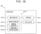
- FIG. 1B is a hardware block diagram of the control circuit according to the first embodiment.
- the control circuit 201 includes a processor 2011, a main storage unit 2012, an auxiliary storage unit 2013, an input-output interface 2014, and a bus 2015 that connects the above-described modules.
- the processor 2011 is a central processing unit that controls the operations of the respective units of control circuit 201.
- the processor 2011 is a CPU, a digital signal processor (DSP), an application specific integrated circuit (ASIC), or the like.
- the processor 2011 develops the program stored in the auxiliary storage unit 2013 in a work area of the main storage unit 2012 in an executable manner.
- the main storage unit 2012 stores a program executed by the processor 2011, data processed by the processor, and the like.
- the main storage unit 2012 is a flash memory, a random access memory (RAM), or the like.
- the auxiliary storage unit 2013 stores various programs and various data.
- the auxiliary storage unit 2013 stores, for example, an operating system (OS), various programs such as a temperature control program 2013a, and various data such as a threshold temperature 2013b.
- the auxiliary storage unit 2013 is a silicon disk including a nonvolatile semiconductor memory (flash memory, erasable programmable read-only memory (EPROM), a solid state drive device, a hard disk (HDD
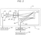
- FIG. 2 is a diagram illustrating a configuration example of the absorbance measurement unit that conducts an absorption analysis with the analysis device according to the first embodiment.
- the irradiation light generated from the light source unit 301 for absorption analysis is emitted along an optical axis 401, focused by a focusing lens 403, and applied to the reaction cells 108.
- a light source-side slit 402 may be provided in order to make the light amount distribution in a light-irradiation plane uniform, and the width of the emitted light from the light source unit 301 may be limited.
- the light transmitted through the reaction solutions 107 in the reaction cells 108 is dispersed by a diffraction grating 3021 in a spectrometer 302 and received by a detector array 3022 including a large number of light receivers.
- a spectrometer-side slit 404 may be disposed to prevent such stray light from entering the spectrometer 302.
- the amounts of components such as proteins, sugars, and lipids contained in the sample 101 are calculated by the following procedure.
- the control circuit 201 instructs the reaction cell cleaning unit 114 to clean the reaction cells 108.
- the control circuit 201 then causes the sample dispensing mechanism 110 to pipet a constant amount of the samples 101 in the sample cups 102 into the reaction cells 108.
- the control circuit 201 then causes the reagent dispensing mechanism 111 to pipet the constant amounts of the reagents 104 in the reagent bottles 105 into the reaction cells 108.
- the control circuit 201 causes the solution stirring unit 112 to stir the samples 101 and the reagents 104 dispensed respectively into the reaction cells 108, thereby generating the reaction solutions 107.
- the rotation of the reaction disk 109 causes the reaction cells 108 containing the reaction solutions 107 to pass through the measurement position where the absorbance measurement unit 113 is disposed.
- the amount of transmitted light from the reaction solution 107 contained in that reaction cell 108 is measured via the absorbance measurement unit 113.
- the measurement data is sequentially output to the information recording unit 2031 and accumulated as reaction process data.
- reaction process data acquired at regular time intervals is stored in the information recording unit 2031.
- FIG. 3 illustrates an example of a detailed configuration of the light source unit according to the first embodiment.
- the light emission side is referred to as an "emission side", and the opposite side is referred to as a "back side”.
- the phosphor 502 is excited by the light generated from an excitation light LED 501, and light is emitted from the phosphor 502.
- the excitation light LED 501 and the phosphor 502 are mounted on an LED package 503.
- the LED package 503 is mounted on an LED mounting board 504.
- a temperature sensor 505 as well as the LED package 503 is mounted on the LED mounting board 504.
- the LED mounting board 504 is a metal-based board using aluminum, copper, or the like with good thermal conductivity.
- the temperature sensor 505 is, for example, a thermistor, a thermocouple, a resistance thermometer sensor, or a semiconductor sensor.
- the heat absorbing side of a Peltier element 506 comes in contact with the back surface of the LED mounting board 504.
- the heat dissipation side of the Peltier element 506 comes in contact with a sub-base 507.
- the sub-base (holding member) 507 is detachable from a lamp house 508 and holds the LED mounting board 504 and the like.
- the Peltier element 506 absorbs heat of the LED mounting board 504 or dissipates heat to the LED mounting board 504.
- the sub-base 507 comes in contact with the inner wall of the lamp house 508. Therefore, the sub-base 507 and the lamp house 508 have the same temperature.
- the sub-base 507 is desirably made of metal from the viewpoint of thermal conductivity, and aluminum, copper, stainless steel, or the like is a candidate for the member.
- a through hole 509 through which the light emitted from the phosphor 502 passes is provided on the emission side of the lamp house 508.
- Optical systems such as the focusing lens 403, a light beam cut filter, the light source-side slit 402, and the spectrometer-side slit 404, may be provided in the through hole 509. With this configuration, the airtightness of air inside the lamp house 508 is improved by the optical systems provided in the through hole 509, and the characteristics of the emitted light can be adjusted.
- a channel 511 for the thermostatic circulating water 115 is provided inside the lamp house 508.
- the channel 511 is a thermostatic mechanism that keeps the temperature of the lamp house 508 constant.
- the thermostatic circulating water 115 is thermostatic circulating water circulating in the thermostatic water bath of the reaction disk 109 illustrated in FIG. 1A , and is adjusted to, for example, 37 ⁇ 0.1°C.
- the channel 511 is made of, for example, stainless steel.
- the metal block of the lamp house 508 is, for example, copper.
- the constituent materials of the channel 511 and the lamp house 508 are not limited to the above, and may be other metals, ceramics, resin, or the like as long as corrosion resistance and thermal conductivity can be secured.
- the temperature of the LED mounting board 504 is desirably higher than the temperature of the lamp house 508 (here, close to 37°C of the thermostatic circulating water), and is, for example, 40°C or higher. In order not to exceed the maximum allowable value of the junction temperature of the excitation light LED 501, the temperature of the LED mounting board 504 is desirably, for example, 60°C or lower. If the airtightness in the lamp house 508 is increased, the possibility of condensation decreases even when the temperature of the LED package 503 is 40°C or lower. However, in consideration of the exchangeability of the LED package 503, it is difficult to completely prevent exchange of air inside and outside the lamp house 508.
- the user turns on the power of the device (step S401).
- the control circuit 201 and the like are energized, and the control circuit 201 and the like are activated.
- the user turns on the power of the light source unit 301 (step S402).
- the excitation light LED 501 emits light.
- the power of the light source unit 301 may be turned on in conjunction with turning on the power of the device.
- step S406 the absorption analysis is started (step S407).
- a blue LED having a center wavelength of 385 nm was used as the excitation light LED 501.
- a white LED (driven at a current of 400 mA) using the phosphor 502 excited by the excitation light was used.
- the LED package 503 was mounted on the LED mounting board 504 as in the configuration example of FIG. 3 .
- the output from the Peltier element 506 was controlled using a thermistor as the temperature sensor 505.
- the threshold temperature Th of the thermistor during the operation of the Peltier element 506 was set to 50.0°C.
- the LED mounting board 504 was an aluminum board on which pattern wiring was formed via an insulating film (resist).
- the temperature fluctuation range of the LED mounting board 504 was compared between a case where the Peltier element 506 was operated and a case where it was not operated. As a result, as shown in Table 1, the temperature fluctuation range was less than 0.01°C when the Peltier element 506 was operated, whereas the temperature fluctuation range was 0.05°C when the Peltier element 506 was not operated. From this result, it was confirmed that the temperature of the LED mounting board 504 was kept constant by the operation of the Peltier element 506.
- the periphery of the LED package 503 is less susceptible to an environmental temperature. Controlling the output from the Peltier element 506 makes it possible to keep the temperature of the LED mounting board 504 on which the LED package 503 is mounted constant. As a result, the changes in the emission spectrum and the light amount of the emitted light from the LED package 503 can be suppressed.
- the Peltier element 506 When output from the Peltier element 506 is controlled so that the temperature measured by the temperature sensor 505 becomes higher than the threshold temperature, the amount of saturated water vapor in the lamp house 508 increases. This can prevent condensation on the LED package 503.
- the threshold temperature Th By setting the threshold temperature Th to a temperature between 40°C to 60°C higher than that of the lamp house 508, it is possible to prevent condensation of the excitation light LED 501 and the phosphor 502 at a temperature lower than the junction temperature of the excitation light LED 501.
- FIG. 5 illustrates an example of a detailed configuration of a light source unit according to a second embodiment.
- the structure of the contact portion between the lamp house 508 and the sub-base 507 is different between the first embodiment and the second embodiment.
- the notch 520 is provided on an outer wall surface of the lamp house 508.
- a protrusion 521 is provided at a position corresponding to the notch 520 of a flange portion 512 of the sub-base 507. When the protrusion 521 comes into contact with the notch 520, the position of the sub-base 507 is determined with respect to the lamp house 508. Since a part of the structure other than the contact portion described above is similar to that of the first embodiment, the description thereof will be omitted.
- FIG. 6 illustrates an example of a detailed configuration of a light source unit according to a third embodiment.
- the sub-base 507 has a heat insulating portion 530.
- the heat insulating portion 530 is provided between a portion holding the LED mounting board 504 and a portion in contact with the lamp house 508.
- This heat insulating portion 530 thermally interrupts a portion in contact with the LED mounting board 504 and the heat absorbing side of the Peltier element 506 to conduct heat, and a portion in contact with the lamp house 508 and the heat dissipating side of the Peltier element 506 to conduct heat.
- the heat insulating portion 530 is made of resin or the like having low thermal conductivity.
- the Peltier element 506 can transfer the heat of the LED mounting board 504 to the inner wall of the lamp house 508 via the sub-base 507.
- the heat insulating portion 530 interferes heat transfer from the flange portion 512 of the sub-base 507 to the lamp house 508.
- the Peltier element 506 is brought into contact with the inner wall of the lamp house 508 and the sub-base 507 and the heat insulating portion 530 is provided. Thereby, heat can be efficiently transferred between the LED mounting board 504 and the inner wall of the lamp house 508. Thus, the temperature of the LED package 503 can be easily kept constant and higher than the threshold temperature.
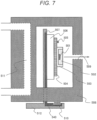
- FIG. 7 illustrates an example of a detailed configuration of a light source unit according to a fourth embodiment.
- the back side of the sub-base 507 does not comes in contact with the inner wall of the lamp house 508.
- heat is conducted from the LED mounting board 504 to the lamp house 508 via the flange portion 512 of the sub-base 507.
- the thermal conductivity does not have to be improved by bringing the back surface side of the sub-base 507 into contact with the inner wall of the lamp house 508.
- the LED package 503 and the LED mounting board 504 can be replaced only by pulling out the sub-base 507 toward the flange portion 512.
- FIG. 8 is a flowchart illustrating an example of a temperature control method of an LED mounting board according to a fifth embodiment.
- the LED mounting board 504 is preheated in order to shorten the time from when the excitation light LED 501 is turned on until the emitted light from the excitation light LED 501 is stabilized.
- a user turns on the power of the device (step S401).
- the control circuit 201 and the like are energized, and the control circuit 201 and the like are activated. Thereafter, the user turns on the power of the light source unit 301 (step S402).
Landscapes
- Physics & Mathematics (AREA)
- Biochemistry (AREA)
- Health & Medical Sciences (AREA)
- Life Sciences & Earth Sciences (AREA)
- Chemical & Material Sciences (AREA)
- Analytical Chemistry (AREA)
- Spectroscopy & Molecular Physics (AREA)
- General Health & Medical Sciences (AREA)
- General Physics & Mathematics (AREA)
- Immunology (AREA)
- Pathology (AREA)
- Investigating Or Analysing Materials By Optical Means (AREA)
- Automatic Analysis And Handling Materials Therefor (AREA)
Abstract
Description
- The present disclosure relates to an analysis device including a light-emitting diode (LED) light source that generates light with which a sample is irradiated.
- In an analysis device that measures the amount of components, such as protein, sugar, lipid, enzyme, hormone, inorganic ion, or disease marker, contained in a sample, such as blood or urine, a sample and a reagent are, in general, dispensed into containers for storing a liquid. Then, test items are analyzed based on changes in optical characteristics such as light absorption, fluorescence, and luminescence. In the absorption analysis with the analysis device, a following method is used. Light from a light source is emitted to a sample or a reaction solution obtained by mixing the sample and a reagent. Then a light receiving element measures the amount of transmitted light with a single or a plurality of measurement wavelengths, the transmitted light having passed through the sample or the reaction solution, to calculate absorbance. The amount of a component is obtained based on a relationship between the absorbance and concentration.
- The light source for the absorption analysis desirably has a wide emission spectrum to cope with a large number of inspection items, and can stably obtain a certain or more light amount at a measurement wavelength in order to conduct highly accurate absorbance measurement. Therefore, conventionally, a xenon lamp, a halogen lamp, or the like has been used. These light sources can obtain a certain or more light amount, but in a case of being used in continuous lighting, the time until the light amount is stabilized is about 30 minutes which is comparatively long. Further, as the light amount is large, the energy consumption is also large, and the life is limited. For example, in a case of a halogen lamp, replacement in about 1000 hours is required, and the maintenance frequency of an analysis device increases.
- In recent years, a light-emitting diode (LED) expected to have a long life has been studied as the light source for the absorption analysis. For example, in an automatic blood analysis device used for a clinical test, a reagent to be used and a wavelength of light vary depending on a component to be measured, and a wavelength range thereof is for example, 340 nm to 800 nm which is wide. Therefore, it is difficult to cover the entire wavelength band with one LED light. For this reason, for example, it is conceivable to use a plurality of LED elements or to use light emission from a phosphor that converts excitation light of a blue LED element to generate light in a long wavelength band.
-
PTL 1 discloses a technique of providing a phosphor on a light beam of an LED chip. The phosphor disclosed inPTL 1 is produced by firing a raw material containing at least alumina and at least one of Fe, Cr, Bi, Tl, Ce, Tb, Eu, and Mn, and containing 6.1 wt% to 15.9 wt% of sodium in the whole raw material. - In the case of using an LED as the light source for the absorption analysis, it is concerned that the emission spectrum and the light amount change depending on self-heating at the time of lighting or an environmental temperature, and thus the analysis accuracy is degraded. In order to prevent this concern, PTL 2 uses a temperature control block in which an LED metering unit and a reaction cell (a member that stores a sample or a reaction solution) comes in contact with each other. The LED is used to make the device compact, and the light-emitting element of the LED is fixed to a member having a large heat capacity to control a preheating temperature. As a result, light amount stability of a certain level or more can be obtained by maintaining the LED element at a temperature within a certain range without being affected by the outside air temperature and self-heating.
- PTL 3 discloses a structure in which a lower surface of an LED package is connected to a Peltier element or a metal block having a channel therein and having good thermal conductivity in order to cool the lower surface and makes it constant to 25 ±0.1°C.
-
- PTL 1:
JP 2020-87974 A - PTL 2:
JP Patent No. 3964291 - PTL 3:
JP Patent No. 6637407 - In order to achieve the light amount stability required for the absorption analysis with an LED light source, the following three problems exist.
-
- (i) In order to suppress changes in the emission spectrum and the light amount due to the self-heating at the time of lighting of the LED light source and the environmental temperature, it is necessary to make the periphery of the LED light source less susceptible to the environmental temperature, and
- (ii) in addition, it is necessary to keep the temperature of a LED mounting board on which the LED light source is mounted constant and to keep the temperature of the LED light source constant.
- (iii) Further, in order to prevent condensation on the LED light source, it is necessary to prevent ambient temperatures of the LED mounting board and the LED light source from decreasing.
- Therefore, an object of the present disclosure is to provide an analysis device including an LED light source capable of suppressing changes in an emission spectrum and a light amount and preventing condensation.
- An analysis device of the present disclosure includes a light-emitting diode (LED) light source configured to generate light with which a sample is irradiated, an LED mounting board on which the LED light source and a temperature sensor are mounted, a lamp house configured to surround a periphery of the LED mounting board and contain the LED mounting board, a Peltier element configured to absorb heat of the LED mounting board or dissipate heat to the LED mounting board, and a control unit configured to control an output from the Peltier element so that a temperature measured by the temperature sensor becomes higher than a threshold temperature.
- According to the present disclosure, the changes in the emission spectrum and the light amount of the LED light source can be suppressed, and condensation can be prevented. Problems, configurations, and effects other than those described above will be clarified by the following description of embodiments.
-
-
FIG. 1A is a schematic diagram illustrating an overall configuration example of an analysis device according to a first embodiment. -
FIG. 1B is a hardware block diagram of a control circuit according to the first embodiment. -
FIG. 2 is a diagram illustrating a configuration example of an absorbance measurement unit that conducts an absorption analysis with the analysis device according to the first embodiment. -
FIG. 3 illustrates an example of a detailed configuration of a light source unit according to the first embodiment. -
FIG. 4 is a flowchart illustrating an example of a temperature control method of a light-emitting diode (LED) mounting board according to the first embodiment. -
FIG. 5 illustrates an example of a detailed configuration of a light source unit according to a second embodiment. -
FIG. 6 illustrates an example of a detailed configuration of a light source unit according to a third embodiment. -
FIG. 7 illustrates an example of a detailed configuration of a light source unit according to a fourth embodiment. -
FIG. 8 is a flowchart illustrating an example of a temperature control method of an LED mounting board according to a fifth embodiment. - Embodiments of the present disclosure will be described in detail with reference to the drawings. In the following embodiments, it goes without saying that components (including element steps and the like) are not necessarily essential unless otherwise specified or considered to be obviously essential in principle.
- Hereinafter, the embodiments of the present disclosure will be described with reference to the drawings.
-
FIG. 1A is a schematic diagram illustrating an overall configuration example of the analysis device using the absorption analysis according to a first embodiment. Theanalysis device 100 according to the present configuration example includes three types of disks including asample disk 103, areagent disk 106, and areaction disk 109, a dispensing mechanism that moves a sample (also referred to as a sample or a specimen) and a reagent between these disks, a control circuit (control unit) 201 that controls these disks and the mechanism, a lightamount measurement circuit 202 that measures absorbance of a reaction solution, adata processing unit 203 that processes data measured by the lightamount measurement circuit 202, and aninput unit 204 and anoutput unit 205 that are interfaces with respect to thedata processing unit 203. The dispensing mechanism includes asample dispensing mechanism 110 and areagent dispensing mechanism 111. - The
data processing unit 203 includes aninformation recording unit 2031 and ananalysis unit 2032. Theinformation recording unit 2031 stores control data, measurement data, data used for data analysis, analysis result data, and the like. Thedata processing unit 203 may be implemented by using a computer. The computer includes at least a processor, such as a central processing unit (CPU), and aninformation recording unit 2031. The processing of theanalysis unit 2032 may be implemented by storing program codes associated with the data processing in theinformation recording unit 2031 and by the processor executing the program codes. - The
input unit 204 and theoutput unit 205 input and output data to and from theinformation recording unit 2031. Theinput unit 204 is an information input device such as a keyboard, a touch panel, or a numeric keypad. Theoutput unit 205 is a device for a user of the analysis device to check the analysis result, and is, for example, a display or the like. - On the circumference of the
sample disk 103, a plurality of sample cups 102, which is storage containers for thesamples 101, is disposed. Thesample 101 is, for example, blood. On the circumference of thereagent disk 106, a plurality ofreagent bottles 105, which are storage containers for thereagent 104, are disposed. A plurality ofreaction cells 108, which is storage containers of thereaction solution 107 obtained by mixing thesample 101 and thereagent 104, is disposed on the circumference of thereaction disk 109. - The
sample dispensing mechanism 110 is a mechanism used when a certain amount of thesample 101 is moved from the sample cups 102 to thereaction cells 108. Thesample dispensing mechanism 110 includes, for example, a nozzle for discharging or aspirating a solution, a robot that positions and conveys the nozzle to a predetermined position, a pump that discharges or aspirates a solution from or to the nozzle, and a channel connecting the nozzle and the pump. - The
reagent dispensing mechanism 111 is a mechanism used when constant amounts of thereagents 104 are moved from thereagent bottles 105 to thereaction cells 108. Thereagent dispensing mechanism 111 also includes, for example, a nozzle for discharging or aspirating a solution, a robot that positions and conveys the nozzle to a predetermined position, a pump that discharges or aspirates a solution from or to the nozzle, and a channel connecting the nozzle and the pump. - A
solution stirring unit 112 is a mechanism unit that stirs and mixes thesamples 101 and thereagents 104 in thereaction cells 108. A reactioncell cleaning unit 114 is a mechanism unit that discharges thereaction solutions 107 from thereaction cells 108 where the analysis processing has been completed, and then cleans thereaction cells 108. Anext sample 101 is dispensed again from thesample dispensing mechanism 110 to thereaction cells 108 after completion of cleaning. Anew reagent 104 is dispensed from thereagent dispensing mechanism 111 to be used for another reaction processing. - In the
reaction disk 109, thereaction cells 108 are immersed in thermostatic circulating water 115 in a thermostatic water bath where a temperature and a flow rate are controlled. Therefore, the temperatures of thereaction cells 108 and thereaction solutions 107 therein are maintained at a constant temperature by thecontrol circuit 201 even during the movement by thereaction disk 109. An absorbance measurement unit (absorptiometer) 113 that conducts the absorption analysis in the analysis device is disposed on a part of the circumference of thereaction disk 109. -
FIG. 1B is a hardware block diagram of the control circuit according to the first embodiment. Thecontrol circuit 201 includes aprocessor 2011, amain storage unit 2012, anauxiliary storage unit 2013, an input-output interface 2014, and abus 2015 that connects the above-described modules. - The
processor 2011 is a central processing unit that controls the operations of the respective units ofcontrol circuit 201. Theprocessor 2011 is a CPU, a digital signal processor (DSP), an application specific integrated circuit (ASIC), or the like. Theprocessor 2011 develops the program stored in theauxiliary storage unit 2013 in a work area of themain storage unit 2012 in an executable manner. Themain storage unit 2012 stores a program executed by theprocessor 2011, data processed by the processor, and the like. Themain storage unit 2012 is a flash memory, a random access memory (RAM), or the like. Theauxiliary storage unit 2013 stores various programs and various data. Theauxiliary storage unit 2013 stores, for example, an operating system (OS), various programs such as atemperature control program 2013a, and various data such as athreshold temperature 2013b. Theauxiliary storage unit 2013 is a silicon disk including a nonvolatile semiconductor memory (flash memory, erasable programmable read-only memory (EPROM), a solid state drive device, a hard disk (HDD) device, or the like. -
FIG. 2 is a diagram illustrating a configuration example of the absorbance measurement unit that conducts an absorption analysis with the analysis device according to the first embodiment. The irradiation light generated from thelight source unit 301 for absorption analysis is emitted along anoptical axis 401, focused by a focusinglens 403, and applied to thereaction cells 108. At this time, a light source-side slit 402 may be provided in order to make the light amount distribution in a light-irradiation plane uniform, and the width of the emitted light from thelight source unit 301 may be limited. - The light transmitted through the
reaction solutions 107 in thereaction cells 108 is dispersed by adiffraction grating 3021 in aspectrometer 302 and received by adetector array 3022 including a large number of light receivers. At this time, since light that has not passed through thereaction solution 107 causes noise, a spectrometer-side slit 404 may be disposed to prevent such stray light from entering thespectrometer 302. - Examples of the measurement wavelength received by the
detector array 3022 include 340 nm, 376 nm, 405 nm, 415 nm, 450 nm, 480 nm, 505 nm, 546 nm, 570 nm, 600 nm, 660 nm, 700 nm, 750 nm, and 800 nm. The light reception signals from an optical receiver are transmitted to theinformation recording unit 2031 of thedata processing unit 203 through the lightamount measurement circuit 202. - The amounts of components such as proteins, sugars, and lipids contained in the
sample 101 are calculated by the following procedure. First, thecontrol circuit 201 instructs the reactioncell cleaning unit 114 to clean thereaction cells 108. Thecontrol circuit 201 then causes thesample dispensing mechanism 110 to pipet a constant amount of thesamples 101 in the sample cups 102 into thereaction cells 108. Thecontrol circuit 201 then causes thereagent dispensing mechanism 111 to pipet the constant amounts of thereagents 104 in thereagent bottles 105 into thereaction cells 108. - At the time of dispensing each solution, the
control circuit 201 rotationally drives thesample disk 103, thereagent disk 106, and thereaction disk 109 with the corresponding drive units. At this time, the sample cups 102, thereagent bottles 105, and thereaction cells 108 are positioned at predetermined dispensing positions in accordance with corresponding drive timings of the dispensing mechanisms. - Subsequently, the
control circuit 201 causes thesolution stirring unit 112 to stir thesamples 101 and thereagents 104 dispensed respectively into thereaction cells 108, thereby generating thereaction solutions 107. The rotation of thereaction disk 109 causes thereaction cells 108 containing thereaction solutions 107 to pass through the measurement position where theabsorbance measurement unit 113 is disposed. Each time thereaction cell 108 passes through the measurement position, the amount of transmitted light from thereaction solution 107 contained in thatreaction cell 108 is measured via theabsorbance measurement unit 113. The measurement data is sequentially output to theinformation recording unit 2031 and accumulated as reaction process data. - During the accumulation of the reaction process data, if necessary, another
reagent 104 is additionally dispensed into thereaction cells 108 by thereagent dispensing mechanism 111, stirred by thesolution stirring unit 112, and further measured for a constant period of time. As a result, reaction process data acquired at regular time intervals is stored in theinformation recording unit 2031. -
FIG. 3 illustrates an example of a detailed configuration of the light source unit according to the first embodiment. In the following description, as illustrated in the drawings, the light emission side is referred to as an "emission side", and the opposite side is referred to as a "back side". Thephosphor 502 is excited by the light generated from anexcitation light LED 501, and light is emitted from thephosphor 502. Theexcitation light LED 501 and thephosphor 502 are mounted on anLED package 503. TheLED package 503 is mounted on anLED mounting board 504. - A
temperature sensor 505 as well as theLED package 503 is mounted on theLED mounting board 504. TheLED mounting board 504 is a metal-based board using aluminum, copper, or the like with good thermal conductivity. Thetemperature sensor 505 is, for example, a thermistor, a thermocouple, a resistance thermometer sensor, or a semiconductor sensor. The heat absorbing side of aPeltier element 506 comes in contact with the back surface of theLED mounting board 504. The heat dissipation side of thePeltier element 506 comes in contact with a sub-base 507. The sub-base (holding member) 507 is detachable from alamp house 508 and holds theLED mounting board 504 and the like. ThePeltier element 506 absorbs heat of theLED mounting board 504 or dissipates heat to theLED mounting board 504. The sub-base 507 comes in contact with the inner wall of thelamp house 508. Therefore, the sub-base 507 and thelamp house 508 have the same temperature. The sub-base 507 is desirably made of metal from the viewpoint of thermal conductivity, and aluminum, copper, stainless steel, or the like is a candidate for the member. - A through
hole 509 through which the light emitted from thephosphor 502 passes is provided on the emission side of thelamp house 508. Optical systems, such as the focusinglens 403, a light beam cut filter, the light source-side slit 402, and the spectrometer-side slit 404, may be provided in the throughhole 509. With this configuration, the airtightness of air inside thelamp house 508 is improved by the optical systems provided in the throughhole 509, and the characteristics of the emitted light can be adjusted. - The structure of the contact portion between the
lamp house 508 and the sub-base 507 will be described. As illustrated inFIG. 3 , aprotrusion 510 protruding outward is provided on an outer wall surface of thelamp house 508. Anotch 513 is provided at a position corresponding to theprotrusion 510 of aflange portion 512 of the sub-base 507. When theprotrusion 510 comes in contact to thenotch 513, the position of the sub-base 507 is determined with respect to thelamp house 508. - As the
lamp house 508, one having good thermal conductivity such as a metal block is used. Achannel 511 for the thermostatic circulating water 115 is provided inside thelamp house 508. Thechannel 511 is a thermostatic mechanism that keeps the temperature of thelamp house 508 constant. The thermostatic circulating water 115 is thermostatic circulating water circulating in the thermostatic water bath of thereaction disk 109 illustrated inFIG. 1A , and is adjusted to, for example, 37±0.1°C. Thechannel 511 is made of, for example, stainless steel. The metal block of thelamp house 508 is, for example, copper. The constituent materials of thechannel 511 and thelamp house 508 are not limited to the above, and may be other metals, ceramics, resin, or the like as long as corrosion resistance and thermal conductivity can be secured. - In order to prevent condensation on the
excitation light LED 501 and thephosphor 502, the temperature of theLED mounting board 504 is desirably higher than the temperature of the lamp house 508 (here, close to 37°C of the thermostatic circulating water), and is, for example, 40°C or higher. In order not to exceed the maximum allowable value of the junction temperature of theexcitation light LED 501, the temperature of theLED mounting board 504 is desirably, for example, 60°C or lower. If the airtightness in thelamp house 508 is increased, the possibility of condensation decreases even when the temperature of theLED package 503 is 40°C or lower. However, in consideration of the exchangeability of theLED package 503, it is difficult to completely prevent exchange of air inside and outside thelamp house 508. In order to generally prevent condensation, it is desirable that the temperature of theLED mounting board 504 is higher than the temperature of thelamp house 508. In particular, in an automatic analysis device that measures the amount of a component contained in a sample such as blood or urine, thermostatic circulating water in the thermostatic water bath whose temperature and flow rate are controlled is often abundantly present in the device, and the humidity is high. Therefore, it is effective to keep the temperature of theLED mounting board 504 higher than the temperature of thelamp house 508 for preventing condensation. In a case where the reaction disk rotates, the surrounding air may circulate to cause high temperature and humidity in the analysis device. -
FIG. 4 is a flowchart illustrating an example of a temperature control method of the LED mounting board according to the first embodiment. In order to stably obtain the analysis performance of the absorption analysis with theanalysis device 100, it is preferable that the amount of light emitted from theLED package 503 is always constant. As means for keeping the light amount constant, according to the configuration of the present disclosure, the output from thePeltier element 506 is controlled based on the temperature of theLED mounting board 504, the temperature being measured by thetemperature sensor 505. Theprocessor 2011 of thecontrol circuit 201 executes thetemperature control program 2013a to execute the processing in steps S403 to S407 inFIG. 4 . - As illustrated in the flowchart of
FIG. 4 , in the absorption analysis with theanalysis device 100 ofFIG. 1A , the user turns on the power of the device (step S401). As a result, thecontrol circuit 201 and the like are energized, and thecontrol circuit 201 and the like are activated. Further, the user turns on the power of the light source unit 301 (step S402). As a result, theexcitation light LED 501 emits light. Note that the power of thelight source unit 301 may be turned on in conjunction with turning on the power of the device. - The
control circuit 201 that has been activated acquires temperature data measured by the temperature sensor 505 (step S403). Thecontrol circuit 201 then controls the output from thePeltier element 506 based on the temperature data acquired from the temperature sensor 505 (step S404) . Specifically, thecontrol circuit 201 controls the output from thePeltier element 506 so that the temperature measured by thetemperature sensor 505 becomes higher than a threshold temperature Th. The threshold temperature Th is, for example, thethreshold temperature 2013b stored in theauxiliary storage unit 2013. - The threshold temperature Th may be a preset value V. The threshold temperature Th may also be a value (Th = S (for example, 37°C) + α (for example, 13°C)) depending on a set temperature S for adjusting the temperature of the thermostatic circulating water 115. The threshold temperature Th may also be a value (Th = Tw + α) determined based on a temperature Tw measured by a thermometer that measures the temperature of the thermostatic circulating water 115. The threshold temperature Th may also be a value (Th = Tl + α) determined based on a temperature T1 measured by a thermometer that measures the temperature of the
lamp house 508. The temperature data used by thecontrol circuit 201 may be not only the temperature measured by thetemperature sensor 505 installed in thelight source unit 301 but also a temperature obtained by another temperature sensor measuring a device environmental temperature. - Next, the
control circuit 201 controls the operation of theabsorbance measurement unit 113 to conduct absorbance measurement (step S405). The lightamount measurement circuit 202 stores the light amount data obtained by the absorbance measurement in theinformation recording unit 2031. Thecontrol circuit 201 then acquires the light amount data from theinformation recording unit 2031. Thecontrol circuit 201 then determines whether the light amount data falls within a light amount fluctuation in a prescribed range required for absorption analysis (step S406). As a result of the determination, in a case where the light amount data does not fall within the light amount fluctuation in the prescribed range (step S406: No), thecontrol circuit 201 returns to the processing in step S404 and controls the output from thePeltier element 506 based on the temperature data acquired from thetemperature sensor 505. - As a result of the determination, in a case where the light amount data falls within the light amount fluctuation in the prescribed range (step S406: Yes), the absorption analysis is started (step S407).
- A blue LED having a center wavelength of 385 nm was used as the
excitation light LED 501. A white LED (driven at a current of 400 mA) using thephosphor 502 excited by the excitation light was used. TheLED package 503 was mounted on theLED mounting board 504 as in the configuration example ofFIG. 3 . The output from thePeltier element 506 was controlled using a thermistor as thetemperature sensor 505. - The threshold temperature Th of the thermistor during the operation of the
Peltier element 506 was set to 50.0°C. TheLED mounting board 504 was an aluminum board on which pattern wiring was formed via an insulating film (resist). When theexcitation light LED 501 was turned on, the temperature fluctuation range of theLED mounting board 504 was compared between a case where thePeltier element 506 was operated and a case where it was not operated. As a result, as shown in Table 1, the temperature fluctuation range was less than 0.01°C when thePeltier element 506 was operated, whereas the temperature fluctuation range was 0.05°C when thePeltier element 506 was not operated. From this result, it was confirmed that the temperature of theLED mounting board 504 was kept constant by the operation of thePeltier element 506. Even when thePeltier element 506 was not in operation, a temperature fluctuation range was 0.05°C which was comparatively small, and the periphery of the LED was surrounded by thelamp house 508. Therefore, it was considered that the temperature of theLED mounting board 504 was less susceptible to the ambient temperature outside the lamp house. Note that since the control temperature of theLED mounting board 504 was set to 50.0°C, no condensation was observed in the LED light source.[Table 1] Condition Temperature fluctuation range of LED mounting board (1) Peltier element was operated less than 0.01°C (2) Peltier element was not operated 0.05°C - Since the
lamp house 508 surrounds the periphery of theLED mounting board 504 and contains theLED mounting board 504, the periphery of theLED package 503 is less susceptible to an environmental temperature. Controlling the output from thePeltier element 506 makes it possible to keep the temperature of theLED mounting board 504 on which theLED package 503 is mounted constant. As a result, the changes in the emission spectrum and the light amount of the emitted light from theLED package 503 can be suppressed. - When output from the
Peltier element 506 is controlled so that the temperature measured by thetemperature sensor 505 becomes higher than the threshold temperature, the amount of saturated water vapor in thelamp house 508 increases. This can prevent condensation on theLED package 503. - The
channel 511 is formed in thelamp house 508, and the thermostatic circulating water 115 is allowed to flow in thechannel 511, so that the temperature of thelamp house 508 can be kept constant. This can suppress the influence of the environmental temperature on thelamp house 508. - The
Peltier element 506 is disposed between theLED mounting board 504 and the sub-base 507 in contact with the inner wall of thelamp house 508. As a result, heat can be easily transferred between thelamp house 508 and theLED mounting board 504, and the temperature of theLED mounting board 504 can be kept constant. - The position of the sub-base 507 with respect to the
lamp house 508 can be determined by making thenotch 513 of the sub-base 507 touch theprotrusion 510 of thelamp house 508. As a result, the position of theLED package 503 held in the sub-base 507 is determined, the position of thephosphor 502 held on theLED package 503 is determined, and the optical axis of the emitted light can be easily determined. - Providing the optical systems in the through
hole 509 of thelamp house 508 improves the airtightness of thelamp house 508. - By setting the threshold temperature Th to a temperature between 40°C to 60°C higher than that of the
lamp house 508, it is possible to prevent condensation of theexcitation light LED 501 and thephosphor 502 at a temperature lower than the junction temperature of theexcitation light LED 501. -
FIG. 5 illustrates an example of a detailed configuration of a light source unit according to a second embodiment. The structure of the contact portion between thelamp house 508 and the sub-base 507 is different between the first embodiment and the second embodiment. As illustrated inFIG. 5 , in the second embodiment, thenotch 520 is provided on an outer wall surface of thelamp house 508. Aprotrusion 521 is provided at a position corresponding to thenotch 520 of aflange portion 512 of the sub-base 507. When theprotrusion 521 comes into contact with thenotch 520, the position of the sub-base 507 is determined with respect to thelamp house 508. Since a part of the structure other than the contact portion described above is similar to that of the first embodiment, the description thereof will be omitted. - The position of the sub-base 507 with respect to the
lamp house 508 can be determined by making theprotrusion 521 of the sub-base 507 touch thenotch 520 of thelamp house 508. As a result, the position of theLED package 503 held in the sub-base 507 is determined and the position of thephosphor 502 held on theLED package 503 is determined. Therefore, the optical axis of the emitted light can be easily determined. - <Third embodiment>
-
FIG. 6 illustrates an example of a detailed configuration of a light source unit according to a third embodiment. In the third embodiment, unlike the first embodiment, the sub-base 507 has aheat insulating portion 530. Theheat insulating portion 530 is provided between a portion holding theLED mounting board 504 and a portion in contact with thelamp house 508. Thisheat insulating portion 530 thermally interrupts a portion in contact with theLED mounting board 504 and the heat absorbing side of thePeltier element 506 to conduct heat, and a portion in contact with thelamp house 508 and the heat dissipating side of thePeltier element 506 to conduct heat. Theheat insulating portion 530 is made of resin or the like having low thermal conductivity. With this structure, thePeltier element 506 can transfer the heat of theLED mounting board 504 to the inner wall of thelamp house 508 via thesub-base 507. Theheat insulating portion 530 interferes heat transfer from theflange portion 512 of the sub-base 507 to thelamp house 508. - The
Peltier element 506 is fixed in thelamp house 508. The sub-base 507 is configured to be detachable from thelamp house 508 with thePeltier element 506 being left in thelamp house 508. As a result, for example, even when theLED mounting board 504 and the sub-base 507 are removed from thelamp house 508 due to the lifetime of theexcitation light LED 501 and theLED package 503 and theLED mounting board 504 are replaced, it is not necessary to remove thePeltier element 506 from the inside of thelamp house 508. Since the other part of the configuration is similar to that in the first embodiment, the description thereof will be omitted. - The
Peltier element 506 is brought into contact with the inner wall of thelamp house 508 and the sub-base 507 and theheat insulating portion 530 is provided. Thereby, heat can be efficiently transferred between theLED mounting board 504 and the inner wall of thelamp house 508. Thus, the temperature of theLED package 503 can be easily kept constant and higher than the threshold temperature. -
FIG. 7 illustrates an example of a detailed configuration of a light source unit according to a fourth embodiment. In the fourth embodiment, the back side of the sub-base 507 does not comes in contact with the inner wall of thelamp house 508. In the fourth embodiment, heat is conducted from theLED mounting board 504 to thelamp house 508 via theflange portion 512 of the sub-base 507. With this structure, the thermal conductivity does not have to be improved by bringing the back surface side of the sub-base 507 into contact with the inner wall of thelamp house 508. Thus, theLED package 503 and theLED mounting board 504 can be replaced only by pulling out the sub-base 507 toward theflange portion 512. Further, aheat conducting path 540 made of a member having high thermal conductivity such as copper is provided in the sub-base 507. Thereby, heat conductivity from the heat dissipation portion of thePeltier element 506 to thelamp house 508 is improved, and temperature controllability of thePeltier element 506 can be improved. Since the other part of the configuration is similar to that in the first embodiment, the description thereof will be omitted. - By attaching the sub-base 507 to the
lamp house 508 without contacting with the inner wall of thelamp house 508, the detachability of the sub-base 507 is improved. Further the temperature of theLED mounting board 504 can be easily controlled by providing theheat conducting path 540. -
FIG. 8 is a flowchart illustrating an example of a temperature control method of an LED mounting board according to a fifth embodiment. In the fifth embodiment, theLED mounting board 504 is preheated in order to shorten the time from when theexcitation light LED 501 is turned on until the emitted light from theexcitation light LED 501 is stabilized. As illustrated in the flowchart ofFIG. 8 , in the absorption analysis with theanalysis device 100 ofFIG. 1A , a user turns on the power of the device (step S401). As a result, thecontrol circuit 201 and the like are energized, and thecontrol circuit 201 and the like are activated. Thereafter, the user turns on the power of the light source unit 301 (step S402). In fifth embodiment, before the user turns on the power of thelight source unit 301, thecontrol circuit 201 controls the output from thePeltier element 506 based on the temperature data acquired from thetemperature sensor 505, and preheats the LED mounting board 504 (step S800). Since the processing thereafter is similar to that in the first embodiment, the description thereof will be omitted. - In the fifth embodiment, by preheating the
LED mounting board 504, the output from thePeltier element 506 is smaller than that in a case where preheating is not performed, and the time to temperature stabilization is also shortened. - Note that the present disclosure is not limited to the above-described embodiments, and includes various modifications. For example, the above-described embodiments have been described in detail for easy understanding of the present disclosure, and are not necessarily limited to those having all the described configurations. A part of the configuration of one embodiment can be replaced with the configuration of another embodiment, and the configuration of the another embodiment can be added to the configuration of one embodiment. The another configuration can be added to and deleted from a part of the configuration in each embodiment, and a part of the configuration in each embodiment can be replaced with the another configurations. Reference Signs List
-
- 100 analysis device
- 101 sample
- 102 sample cup
- 103 sample disk
- 104 reagent
- 105 reagent bottle
- 106 reagent disk
- 107 reaction solution
- 108 reaction cell
- 109 reaction disk
- 110 sample dispensing mechanism
- 111 reagent dispensing mechanism
- 112 solution stirring unit
- 113 absorbance measurement unit
- 114 reaction cell cleaning unit
- 115 thermostatic circulating water
- 201 control circuit
- 2011 processor
- 2012 main storage unit
- 2013 auxiliary storage unit
- 2013a temperature control program
- 2013b threshold temperature
- 2014 input-output interface
- 2015 bus
- 202 light amount measurement circuit
- 203 data processing unit
- 2031 information recording unit
- 2032 analysis unit
- 204 input unit
- 205 output unit
- 301 light source unit
- 302 spectrometer
- 3021 diffraction grating
- 3022 detector array
- 401 optical axis
- 402 light source-side slit
- 403 focusing lens
- 404 spectrometer-side slit
- 501 excitation light LED
- 502 phosphor
- 503 LED package
- 504 LED mounting board
- 505 temperature sensor
- 506 Peltier element
- 507 sub-base
- 508 lamp house
- 510, 521 protrusion
- 513, 520 notch
- 511 channel
- 530 heat insulating portion
- 540 heat conducting path
Claims (14)
- An analysis device comprising:a light-emitting diode (LED) light source that generates light with which a sample is irradiated;an LED mounting board on which the LED light source and a temperature sensor are mounted;a lamp house configured to surround a periphery of the LED mounting board and contain the LED mounting board;a Peltier element configured to absorb heat of the LED mounting board or dissipate heat to the LED mounting board; anda control unit configured to control an output from the Peltier element so that a temperature measured by the temperature sensor becomes higher than a threshold temperature.
- The analysis device according to claim 1, further comprising a thermostatic mechanism configured to keep a temperature of the lamp house constant.
- The analysis device according to claim 1, wherein the Peltier element is disposed between an inner wall of the lamp house and the LED mounting board.
- The analysis device according to claim 1, further comprising a holding member configured to be detachable from the lamp house and hold the LED mounting board,wherein the holding member has a notch, andthe lamp house has a protrusion to touch the notch.
- The analysis device according to claim 1, further comprising a holding member configured to be detachable from the lamp house and hold the LED mounting board,wherein the lamp house has a notch, andthe holding member has a protrusion that comes into contact with the notch.
- The analysis device according to claim 1, further comprising a holding member configured to be detachable from the lamp house and hold the LED mounting board,wherein the Peltier element is brought into contact with an inner wall of the lamp house and the holding member, andthe holding member includes a heat insulating portion provided between a portion that holds the LED mounting board and a portion that comes in contact with the lamp house.
- The analysis device according to claim 1, further comprising a holding member configured to be detachable from the lamp house and hold the LED mounting board,
wherein the holding member is attached to the lamp house without contacting with an inner wall of the lamp house. - The analysis device according to claim 1, further comprising a holding member configured to be detachable from the lamp house with the Peltier element being left in the lamp house and hold the LED mounting board.
- The analysis device according to claim 1, whereinthe lamp house includes a through hole through which light emitted from the LED light source passes, andthe through hole has an optical system.
- The analysis device according to claim 1, wherein the threshold temperature is a temperature determined based on a temperature of the lamp house.
- The analysis device according to claim 1, wherein the threshold temperature is a temperature between 40°C to 60°C which is higher than a temperature of the lamp house.
- The analysis device according to claim 1, wherein the control unit is configured to control the output from the Peltier element so as to dissipate heat to the LED mounting board before the LED light source emits light.
- The analysis device according to claim 1,wherein the sample is stored in a reaction container,the analysis device further comprising the reaction container and thermostatic circulating water for keeping the sample in the reaction container at a constant temperature.
- The analysis device according to claim 13, comprising:a reaction disk configured to place at least one of the reaction container on a circumference of the reaction disk;a thermostatic water bath in which the reaction container placed on the reaction disk is immersed in the thermostatic circulating water; anda control unit configured to rotationally drive the reaction disk.
Applications Claiming Priority (2)
| Application Number | Priority Date | Filing Date | Title |
|---|---|---|---|
| JP2022092124A JP7767227B2 (en) | 2022-06-07 | 2022-06-07 | Analyzer |
| PCT/JP2023/007481 WO2023238457A1 (en) | 2022-06-07 | 2023-03-01 | Analysis device |
Publications (2)
| Publication Number | Publication Date |
|---|---|
| EP4538678A1 true EP4538678A1 (en) | 2025-04-16 |
| EP4538678A4 EP4538678A4 (en) | 2026-04-29 |
Family
ID=89117964
Family Applications (1)
| Application Number | Title | Priority Date | Filing Date |
|---|---|---|---|
| EP23818221.6A Pending EP4538678A4 (en) | 2022-06-07 | 2023-03-01 | Analysis device |
Country Status (4)
| Country | Link |
|---|---|
| EP (1) | EP4538678A4 (en) |
| JP (1) | JP7767227B2 (en) |
| CN (1) | CN119096132A (en) |
| WO (1) | WO2023238457A1 (en) |
Family Cites Families (12)
| Publication number | Priority date | Publication date | Assignee | Title |
|---|---|---|---|---|
| JP2002101274A (en) * | 2000-09-26 | 2002-04-05 | Fuji Photo Film Co Ltd | Light source device, image reading device, and image reading method |
| JP3964291B2 (en) | 2002-09-06 | 2007-08-22 | 富士フイルム株式会社 | Analytical instrument |
| JP2005175010A (en) | 2003-12-08 | 2005-06-30 | Sysmex Corp | Optical source equipment |
| JP2006156829A (en) | 2004-11-30 | 2006-06-15 | Toshiba Lighting & Technology Corp | Light emitting device |
| JP4670375B2 (en) | 2005-02-03 | 2011-04-13 | パナソニック株式会社 | Imaging device |
| JP2007258520A (en) | 2006-03-24 | 2007-10-04 | Matsushita Electric Ind Co Ltd | Electronic equipment cooling device |
| WO2010117026A1 (en) | 2009-04-08 | 2010-10-14 | 株式会社日立ハイテクノロジーズ | Light source device, analytical device using same, and liquid crystal display device |
| US8845134B2 (en) | 2010-03-05 | 2014-09-30 | Nec Corporation | Cooling system for light emitting device and light emitting device using the same |
| JP2012057944A (en) * | 2010-09-03 | 2012-03-22 | Sumitomo Electric Ind Ltd | Method and apparatus for evaluating light-emitting element |
| JP6637407B2 (en) * | 2016-12-27 | 2020-01-29 | 株式会社日立ハイテクノロジーズ | Automatic analyzer |
| JP7102321B2 (en) * | 2018-11-15 | 2022-07-19 | 株式会社日立ハイテク | Broadband light source device and biochemical analyzer |
| JP7291063B2 (en) * | 2019-11-20 | 2023-06-14 | 株式会社日立ハイテク | automatic analyzer |
-
2022
- 2022-06-07 JP JP2022092124A patent/JP7767227B2/en active Active
-
2023
- 2023-03-01 WO PCT/JP2023/007481 patent/WO2023238457A1/en not_active Ceased
- 2023-03-01 EP EP23818221.6A patent/EP4538678A4/en active Pending
- 2023-03-01 CN CN202380037030.7A patent/CN119096132A/en active Pending
Also Published As
| Publication number | Publication date |
|---|---|
| JP2023179070A (en) | 2023-12-19 |
| EP4538678A4 (en) | 2026-04-29 |
| WO2023238457A1 (en) | 2023-12-14 |
| JP7767227B2 (en) | 2025-11-11 |
| CN119096132A (en) | 2024-12-06 |
Similar Documents
| Publication | Publication Date | Title |
|---|---|---|
| JP7664456B2 (en) | Automated Analysis Equipment | |
| EP2317304B1 (en) | Sample analysis device | |
| CN110073200B (en) | Automatic analyzer | |
| EP4692760A1 (en) | Analysis device, determination method, and prediction method | |
| WO2018051671A1 (en) | Automatic analysis apparatus | |
| JP7638374B2 (en) | Light source and automatic analyzer | |
| JP7767227B2 (en) | Analyzer | |
| JP7546141B2 (en) | Light source and automatic analyzer | |
| WO2024105966A1 (en) | Automated analysis device | |
| JP2026043123A (en) | Analytical device and method for determining the state of an LED light source. |
Legal Events
| Date | Code | Title | Description |
|---|---|---|---|
| STAA | Information on the status of an ep patent application or granted ep patent |
Free format text: STATUS: THE INTERNATIONAL PUBLICATION HAS BEEN MADE |
|
| PUAI | Public reference made under article 153(3) epc to a published international application that has entered the european phase |
Free format text: ORIGINAL CODE: 0009012 |
|
| STAA | Information on the status of an ep patent application or granted ep patent |
Free format text: STATUS: REQUEST FOR EXAMINATION WAS MADE |
|
| 17P | Request for examination filed |
Effective date: 20250107 |
|
| AK | Designated contracting states |
Kind code of ref document: A1 Designated state(s): AL AT BE BG CH CY CZ DE DK EE ES FI FR GB GR HR HU IE IS IT LI LT LU LV MC ME MK MT NL NO PL PT RO RS SE SI SK SM TR |
|
| DAV | Request for validation of the european patent (deleted) | ||
| DAX | Request for extension of the european patent (deleted) | ||
| REG | Reference to a national code |
Ref country code: DE Ref legal event code: R079 Free format text: PREVIOUS MAIN CLASS: G01N0021010000 Ipc: G01N0021250000 |
|
| A4 | Supplementary search report drawn up and despatched |
Effective date: 20260330 |
|
| RIC1 | Information provided on ipc code assigned before grant |
Ipc: G01N 21/25 20060101AFI20260324BHEP |