EP4535227A1 - Ic tag and manufacturing method for same - Google Patents
Ic tag and manufacturing method for same Download PDFInfo
- Publication number
- EP4535227A1 EP4535227A1 EP23815546.9A EP23815546A EP4535227A1 EP 4535227 A1 EP4535227 A1 EP 4535227A1 EP 23815546 A EP23815546 A EP 23815546A EP 4535227 A1 EP4535227 A1 EP 4535227A1
- Authority
- EP
- European Patent Office
- Prior art keywords
- substrate
- protective layer
- chip
- tensile modulus
- antenna
- Prior art date
- Legal status (The legal status is an assumption and is not a legal conclusion. Google has not performed a legal analysis and makes no representation as to the accuracy of the status listed.)
- Pending
Links
Images

Classifications
-
- G—PHYSICS
- G06—COMPUTING OR CALCULATING; COUNTING
- G06K—GRAPHICAL DATA READING; PRESENTATION OF DATA; RECORD CARRIERS; HANDLING RECORD CARRIERS
- G06K19/00—Record carriers for use with machines and with at least a part designed to carry digital markings
- G06K19/02—Record carriers for use with machines and with at least a part designed to carry digital markings characterised by the selection of materials, e.g. to avoid wear during transport through the machine
-
- G—PHYSICS
- G06—COMPUTING OR CALCULATING; COUNTING
- G06K—GRAPHICAL DATA READING; PRESENTATION OF DATA; RECORD CARRIERS; HANDLING RECORD CARRIERS
- G06K19/00—Record carriers for use with machines and with at least a part designed to carry digital markings
- G06K19/06—Record carriers for use with machines and with at least a part designed to carry digital markings characterised by the kind of the digital marking, e.g. shape, nature, code
- G06K19/067—Record carriers with conductive marks, printed circuits or semiconductor circuit elements, e.g. credit or identity cards also with resonating or responding marks without active components
- G06K19/07—Record carriers with conductive marks, printed circuits or semiconductor circuit elements, e.g. credit or identity cards also with resonating or responding marks without active components with integrated circuit chips
- G06K19/077—Constructional details, e.g. mounting of circuits in the carrier
-
- G—PHYSICS
- G06—COMPUTING OR CALCULATING; COUNTING
- G06K—GRAPHICAL DATA READING; PRESENTATION OF DATA; RECORD CARRIERS; HANDLING RECORD CARRIERS
- G06K19/00—Record carriers for use with machines and with at least a part designed to carry digital markings
- G06K19/06—Record carriers for use with machines and with at least a part designed to carry digital markings characterised by the kind of the digital marking, e.g. shape, nature, code
- G06K19/067—Record carriers with conductive marks, printed circuits or semiconductor circuit elements, e.g. credit or identity cards also with resonating or responding marks without active components
- G06K19/07—Record carriers with conductive marks, printed circuits or semiconductor circuit elements, e.g. credit or identity cards also with resonating or responding marks without active components with integrated circuit chips
- G06K19/077—Constructional details, e.g. mounting of circuits in the carrier
- G06K19/0772—Physical layout of the record carrier
- G06K19/07722—Physical layout of the record carrier the record carrier being multilayered, e.g. laminated sheets
-
- G—PHYSICS
- G06—COMPUTING OR CALCULATING; COUNTING
- G06K—GRAPHICAL DATA READING; PRESENTATION OF DATA; RECORD CARRIERS; HANDLING RECORD CARRIERS
- G06K19/00—Record carriers for use with machines and with at least a part designed to carry digital markings
- G06K19/06—Record carriers for use with machines and with at least a part designed to carry digital markings characterised by the kind of the digital marking, e.g. shape, nature, code
- G06K19/067—Record carriers with conductive marks, printed circuits or semiconductor circuit elements, e.g. credit or identity cards also with resonating or responding marks without active components
- G06K19/07—Record carriers with conductive marks, printed circuits or semiconductor circuit elements, e.g. credit or identity cards also with resonating or responding marks without active components with integrated circuit chips
- G06K19/077—Constructional details, e.g. mounting of circuits in the carrier
- G06K19/0772—Physical layout of the record carrier
- G06K19/07728—Physical layout of the record carrier the record carrier comprising means for protection against impact or bending, e.g. protective shells or stress-absorbing layers around the integrated circuit
-
- G—PHYSICS
- G06—COMPUTING OR CALCULATING; COUNTING
- G06K—GRAPHICAL DATA READING; PRESENTATION OF DATA; RECORD CARRIERS; HANDLING RECORD CARRIERS
- G06K19/00—Record carriers for use with machines and with at least a part designed to carry digital markings
- G06K19/06—Record carriers for use with machines and with at least a part designed to carry digital markings characterised by the kind of the digital marking, e.g. shape, nature, code
- G06K19/067—Record carriers with conductive marks, printed circuits or semiconductor circuit elements, e.g. credit or identity cards also with resonating or responding marks without active components
- G06K19/07—Record carriers with conductive marks, printed circuits or semiconductor circuit elements, e.g. credit or identity cards also with resonating or responding marks without active components with integrated circuit chips
- G06K19/077—Constructional details, e.g. mounting of circuits in the carrier
- G06K19/07749—Constructional details, e.g. mounting of circuits in the carrier the record carrier being capable of non-contact communication, e.g. constructional details of the antenna of a non-contact smart card
-
- G—PHYSICS
- G06—COMPUTING OR CALCULATING; COUNTING
- G06K—GRAPHICAL DATA READING; PRESENTATION OF DATA; RECORD CARRIERS; HANDLING RECORD CARRIERS
- G06K19/00—Record carriers for use with machines and with at least a part designed to carry digital markings
- G06K19/06—Record carriers for use with machines and with at least a part designed to carry digital markings characterised by the kind of the digital marking, e.g. shape, nature, code
- G06K19/067—Record carriers with conductive marks, printed circuits or semiconductor circuit elements, e.g. credit or identity cards also with resonating or responding marks without active components
- G06K19/07—Record carriers with conductive marks, printed circuits or semiconductor circuit elements, e.g. credit or identity cards also with resonating or responding marks without active components with integrated circuit chips
- G06K19/077—Constructional details, e.g. mounting of circuits in the carrier
- G06K19/07749—Constructional details, e.g. mounting of circuits in the carrier the record carrier being capable of non-contact communication, e.g. constructional details of the antenna of a non-contact smart card
- G06K19/07773—Antenna details
-
- H—ELECTRICITY
- H01—ELECTRIC ELEMENTS
- H01Q—ANTENNAS, i.e. RADIO AERIALS
- H01Q1/00—Details of, or arrangements associated with, antennas
- H01Q1/12—Supports; Mounting means
- H01Q1/22—Supports; Mounting means by structural association with other equipment or articles
- H01Q1/2208—Supports; Mounting means by structural association with other equipment or articles associated with components used in interrogation type services, i.e. in systems for information exchange between an interrogator/reader and a tag/transponder, e.g. in Radio Frequency Identification [RFID] systems
- H01Q1/2225—Supports; Mounting means by structural association with other equipment or articles associated with components used in interrogation type services, i.e. in systems for information exchange between an interrogator/reader and a tag/transponder, e.g. in Radio Frequency Identification [RFID] systems used in active tags, i.e. provided with its own power source or in passive tags, i.e. deriving power from RF signal
-
- H—ELECTRICITY
- H01—ELECTRIC ELEMENTS
- H01Q—ANTENNAS, i.e. RADIO AERIALS
- H01Q1/00—Details of, or arrangements associated with, antennas
- H01Q1/40—Radiating elements coated with or embedded in protective material
-
- H—ELECTRICITY
- H01—ELECTRIC ELEMENTS
- H01Q—ANTENNAS, i.e. RADIO AERIALS
- H01Q9/00—Electrically-short antennas having dimensions not more than twice the operating wavelength and consisting of conductive active radiating elements
- H01Q9/04—Resonant antennas
- H01Q9/16—Resonant antennas with feed intermediate between the extremities of the antenna, e.g. centre-fed dipole
-
- H—ELECTRICITY
- H01—ELECTRIC ELEMENTS
- H01Q—ANTENNAS, i.e. RADIO AERIALS
- H01Q9/00—Electrically-short antennas having dimensions not more than twice the operating wavelength and consisting of conductive active radiating elements
- H01Q9/04—Resonant antennas
- H01Q9/16—Resonant antennas with feed intermediate between the extremities of the antenna, e.g. centre-fed dipole
- H01Q9/28—Conical, cylindrical, cage, strip, gauze, or like elements having an extended radiating surface; Elements comprising two conical surfaces having collinear axes and adjacent apices and fed by two-conductor transmission lines
- H01Q9/285—Planar dipole
Definitions
- the present invention relates to an IC tag and a manufacturing method therefor.
- Patent Literature 1 WO2009/011041
- the above IC tag may be used in a severe environment in which the IC tag is subjected to external forces such as bending, which may cause the resin for protecting the antenna to peel off and damage the antenna.
- external forces such as bending
- a communication performance may deteriorate or communication may become impossible.
- a laundry tag used for clothes, linen, and the like is required to have durability against repeated washing or drying in a drying machine.
- An IC tag includes: an IC chip; an antenna that electrically transmits and receives information stored in the IC chip; a sheet-like substrate that supports the IC chip and the antenna; and a resin protective layer which is a dielectric covering the IC chip and the antenna between the resin protective layer and the substrate, in which a tensile modulus [GPa] of the substrate and a tensile modulus [GPa] of the protective layer are defined within an area surrounded by five lines represented by the following formulas (1), (2), (3), (4), and (5), with the tensile modulus of the substrate on an X-axis and the tensile modulus of the protective layer on a Y-axis.
- a method for manufacturing an IC tag includes: a step of forming, on a sheet-like substrate, an IC chip and an antenna that electrically transmits and receives information stored in the IC chip; a step of disposing a sheet-like resin material, which is a dielectric, on the substrate to cover the IC chip and the antenna; and a step of forming a protective layer along the IC chip and the antenna on the substrate by heating and pressing the resin material, in which the substrate and the resin material are selected such that a tensile modulus [GPa] of the substrate and a tensile modulus [GPa] of the protective layer are defined within an area surrounded by five lines represented by the following formulas (1), (2), (3), (4), and (5), with the tensile modulus of the substrate on an X-axis and the tensile modulus of the protective layer on a Y-axis.
- a bending resistance of the IC tag can be improved.
- FIG. 1 is a plan view of the IC tag according to the present embodiment
- FIG. 2 is a cross-sectional view of FIG. 1
- the IC tag according to the present embodiment includes a sheet-like substrate 1 formed in a rectangular shape, an IC chip 2 and an antenna 3 disposed on the substrate 1, and a protective layer 4 that is formed in a rectangular shape and that covers the IC chip 2 and the antenna 3.
- a protective layer 4 that is formed in a rectangular shape and that covers the IC chip 2 and the antenna 3.
- the substrate 1 is made of a material having a tensile modulus of 0.8 GPa to 8 GPa.
- the material constituting the substrate 1 is not particularly limited, and can be, for example, a polyester-based resin such as polyethylene, polypropylene, polyvinyl chloride, and polyethylene terephthalate, and a polyimide-based resin.
- a thickness of the substrate 1 is, for example, preferably 25 ⁇ m to 200 ⁇ m, and further preferably 50 ⁇ m to 150 ⁇ m.
- first side 101 and a second side 102 sides of the substrate 1 and the protective layer 4 in a longitudinal direction are referred to as a first side 101 and a second side 102, and sides in a lateral direction are referred to as a third side 103 and a fourth side 104. Therefore, these sides are connected in order of the first side 101, the third side 103, the second side 102, and the fourth side 104.
- the IC chip 2 is known one having a memory function and is electrically connected to the dipole antenna 3 implemented by a conductor.
- the impedance matching portion 31 has the first side 311, a third side 313, the second side 312, and a fourth side 314 connected in this order.
- the IC chip 2 is disposed in the vicinity of a center of the first side 311 of the impedance matching portion 31 or at a position slightly deviated therefrom.
- the dipole portion 32 has a bilaterally symmetrical shape, and thus only a left side in FIG. 1 will be described.
- the dipole portion 32 extends from the first side 311 of the impedance matching portion 31 toward the first side 101 of the substrate 1, extends therefrom along the first side 101, the third side 103, and the second side 102 of the substrate 1, forms a rectangular shape frame along the third side 313 of the impedance matching portion 31, and then extends inside the frame in a spiral shape.
- a thickness of the dipole antenna 3 is not particularly limited, and can be set to 5 ⁇ m to 20 ⁇ m.
- the material constituting the dipole antenna 3 is not particularly limited, and can be, for example, silver, copper, or aluminum.
- the dipole antenna 3 can be formed by applying a silver paste containing silver onto the substrate 1 by screen printing.
- the dipole antenna 3 can be formed by etching.
- the IC chip 2 can be fixed to the antenna 3 with an adhesive, or can be fixed to the antenna 3 by known flip-chip mounting for electronic components.
- a thickness of the IC chip 2 is not particularly limited, and can be set to 100 ⁇ m to 150 ⁇ m.
- information stored in the IC chip 2 can be transmitted and received by radio waves in a UHF band.
- the tensile modulus of the substrate 1 and the tensile modulus of the protective layer 4 are defined within an area surrounded by five lines represented by the following formulas (1), (2), (3), (4), and (5), with the tensile modulus [GPa] of the substrate 1 on the X-axis and the tensile modulus [GPa] of the protective layer 4 on the Y-axis.
- the protective layer 4 may cover the dipole antenna 3 and the IC chip 2, and a thickness from the substrate 1 is, for example, preferably 25 ⁇ m to 150 ⁇ m, and further preferably 50 ⁇ m to 100 ⁇ m.
- the tensile modulus can be measured according to IPC-TM-650.
- the IC tag configured as described above can be formed by using various methods, for example, the following method.
- the dipole antenna 3 is formed on the substrate 1 by using the above method such as screen printing or etching.
- the IC chip 2 is fixed on the dipole antenna 3 by using the above method.
- a sheet-like resin material having the same size as the substrate 1 and serving as the protective layer 4 is disposed on the substrate 1 so as to cover the dipole antenna 3 and the IC chip 2.
- the resin material is pressed while being heated by a plate. Accordingly, the resin material is bonded to the substrate 1 so as to cover the dipole antenna 3 and the IC chip 2 while being deformed to conform to shapes of the dipole antenna 3 and the IC chip 2.
- the IC tag is completed.
- the dipole antenna 3 is formed on the substrate 1 having a tensile modulus of 0.8 GPa to 8 GPa, and the IC chip 2 is fixed on the dipole antenna 3.
- the tensile modulus of the substrate 1 is set to 0.8 GPa or more.
- the tensile modulus of the substrate 1 is set to 8 GPa or less.
- the dipole antenna 3 and the IC chip 2 are covered with only the protective layer 4 in the above embodiment, and a sheet-like cover 5 can be further provided on the protective layer 4 as shown in FIG. 3 .
- the cover 5 can be made of, for example, the same material as the substrate 1.
- a tensile modulus of the cover 5 is, for example, 0.8 GPa to 8 GPa, and a thickness thereof is, for example, preferably 25 ⁇ m to 200 ⁇ m, and further preferably 50 ⁇ m to 150 ⁇ m.
- the cover 5 when the tensile modulus of the cover 5 is 8 GPa or more, the cover 5 may be cracked at the time of bending, and when the tensile modulus is 0.8 GPa or less, an effect of preventing the deformation of the protective layer 4 is reduced. In addition, similar to the interface between the substrate 1 and the protective layer 4, it is also possible to prevent an interface between the protective layer 4 and the cover 5 from being peeled.
- the shape of the dipole antenna 3 is an example, and various shapes can be used.
- a position of the IC chip 2 on the antenna 3 is also not particularly limited.
- various antennas can be used as the antenna 3, and a patch antenna may also be used in addition to the above dipole antenna. That is, the shape or the like of the antenna 3 is not particularly limited, and various forms are possible.
- the shape of the IC tag that is, the shapes of the substrate 1, the protective layer 4, and the cover 5 are not particularly limited, and various shapes such as a rectangular shape, a circular shape, and a polygonal shape can be adopted in accordance with the application in addition to the elongated shape as described above.
- the substrate 1, the protective layer 4, and the cover 5 may not have the same shape.
- IC tags according to Samples 1 to 50 were prepared as follows. Table 1 shows materials, tensile modulus, and thicknesses of substrates used in the production of Samples 1 to 50.
- Table 2 shows materials, tensile modulus, and thicknesses of protective layers used in the production of Samples 1 to 50.
- Samples 1 to 50 shown in Table 3 were produced by changing the combination of the substrates and the protective layers.
- sizes of the substrate, the IC chip, and the dipole antenna are the same. That is, on a rectangular substrate of 33.5 mm ⁇ 7.5 mm made of the material shown in Table 1, an antenna made of silver paste and having a thickness of 10 ⁇ m was formed as shown in FIG. 1 , and an IC chip was fixed thereon with an adhesive.
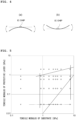
- FIG. 5 is a graph showing the results of the bending test, with the tensile modulus [GPa] of the substrate on an X-axis and the tensile modulus [GPa] of the protective layer on a Y-axis.
- the X-axis represents the tensile modulus [GPa] of the substrate in logarithm
- the Y-axis represents the tensile modulus [GPa] of the protective layer in logarithm
- the results of the bending tests of Samples 1 to 50 are shown in a plot.
- the IC tag according to the present invention has a high bending resistance in the case of being subjected to repeated bending, and is therefore particularly suitable as a laundry tag used for clothes, linen, and the like which are required to have durability against repeated washing or drying in a drying machine. Further, the IC tag is also suitably used for rental mats and mops which are exposed to the repeated washing or chemical treatment.
Landscapes
- Engineering & Computer Science (AREA)
- Physics & Mathematics (AREA)
- General Physics & Mathematics (AREA)
- Theoretical Computer Science (AREA)
- Computer Hardware Design (AREA)
- Microelectronics & Electronic Packaging (AREA)
- Computer Networks & Wireless Communication (AREA)
- Details Of Aerials (AREA)
- Credit Cards Or The Like (AREA)
Abstract





Description
- The present invention relates to an IC tag and a manufacturing method therefor.
- In recent years, as one type of IC tag, there has been proposed a configuration in which an antenna pattern for radio communication and an IC chip are mounted on a base sheet made of plastic or paper called an inlet. Such an inlet sealed with a resin is attached to an article or embedded in the article to be used for managing the article.
- Patent Literature 1:
WO2009/011041 - Incidentally, the above IC tag may be used in a severe environment in which the IC tag is subjected to external forces such as bending, which may cause the resin for protecting the antenna to peel off and damage the antenna. When the antenna is damaged, a communication performance may deteriorate or communication may become impossible. In particular, a laundry tag used for clothes, linen, and the like is required to have durability against repeated washing or drying in a drying machine.
- The present invention has been made to solve the above problem, and an object of the present invention is to provide an IC tag and a manufacturing method therefor which can prevent an antenna from being damaged even when the IC tag is repeatedly subjected to external forces such as bending.
- An IC tag according to the present invention includes: an IC chip; an antenna that electrically transmits and receives information stored in the IC chip; a sheet-like substrate that supports the IC chip and the antenna; and a resin protective layer which is a dielectric covering the IC chip and the antenna between the resin protective layer and the substrate, in which a tensile modulus [GPa] of the substrate and a tensile modulus [GPa] of the protective layer are defined within an area surrounded by five lines represented by the following formulas (1), (2), (3), (4), and (5), with the tensile modulus of the substrate on an X-axis and the tensile modulus of the protective layer on a Y-axis.


- A method for manufacturing an IC tag according to the present invention includes: a step of forming, on a sheet-like substrate, an IC chip and an antenna that electrically transmits and receives information stored in the IC chip; a step of disposing a sheet-like resin material, which is a dielectric, on the substrate to cover the IC chip and the antenna; and a step of forming a protective layer along the IC chip and the antenna on the substrate by heating and pressing the resin material, in which the substrate and the resin material are selected such that a tensile modulus [GPa] of the substrate and a tensile modulus [GPa] of the protective layer are defined within an area surrounded by five lines represented by the following formulas (1), (2), (3), (4), and (5), with the tensile modulus of the substrate on an X-axis and the tensile modulus of the protective layer on a Y-axis.



- According to the IC tag and the manufacturing method therefor according to the present invention, a bending resistance of the IC tag can be improved.
-
-
FIG. 1 is a plan view showing an embodiment of an IC tag according to the present invention. -
FIG. 2 is a cross-sectional view of the IC tag ofFIG. 1 . -
FIG. 3 is a cross-sectional view showing another example of the IC tag ofFIG. 1 . -
FIG. 4 is a view showing a bending test of the IC tag. -
FIG. 5 is a graph showing results of the bending test, with a tensile modulus of a substrate on an X-axis and a tensile modulus of a protective layer on a Y-axis. - Hereinafter, an embodiment of an IC tag according to the present invention will be described with reference to the drawings.
FIG. 1 is a plan view of the IC tag according to the present embodiment, andFIG. 2 is a cross-sectional view ofFIG. 1 . As shown inFIGS. 1 and 2 , the IC tag according to the present embodiment includes a sheet-like substrate 1 formed in a rectangular shape, anIC chip 2 and anantenna 3 disposed on thesubstrate 1, and aprotective layer 4 that is formed in a rectangular shape and that covers theIC chip 2 and theantenna 3. Hereinafter, each member will be described in detail. - The
substrate 1 is made of a material having a tensile modulus of 0.8 GPa to 8 GPa. As long as the tensile modulus is 0.8 GPa to 8 GPa, the material constituting thesubstrate 1 is not particularly limited, and can be, for example, a polyester-based resin such as polyethylene, polypropylene, polyvinyl chloride, and polyethylene terephthalate, and a polyimide-based resin. A thickness of thesubstrate 1 is, for example, preferably 25 µm to 200 µm, and further preferably 50 µm to 150 µm. - Hereinafter, for convenience of description, as shown in
FIG. 1 , sides of thesubstrate 1 and theprotective layer 4 in a longitudinal direction are referred to as afirst side 101 and asecond side 102, and sides in a lateral direction are referred to as athird side 103 and afourth side 104. Therefore, these sides are connected in order of thefirst side 101, thethird side 103, thesecond side 102, and thefourth side 104. - The
IC chip 2 is known one having a memory function and is electrically connected to thedipole antenna 3 implemented by a conductor. - In the present embodiment, the dipole antenna as shown in
FIG. 1 is used as an example. That is, thedipole antenna 3 includes animpedance matching portion 31 disposed in the vicinity of a center in the longitudinal direction of thesubstrate 1, and a pair ofdipole portions 32 extending from theimpedance matching portion 31 in the longitudinal direction of thesubstrate 1. Theimpedance matching portion 31 is formed in a rectangular frame shape having first to fourth sides. More specifically, afirst side 311 of theimpedance matching portion 31 is disposed at a position slightly away from thefirst side 101 of thesubstrate 1, and asecond side 312 is disposed along thesecond side 102 of thesubstrate 1. That is, theimpedance matching portion 31 has thefirst side 311, athird side 313, thesecond side 312, and afourth side 314 connected in this order. TheIC chip 2 is disposed in the vicinity of a center of thefirst side 311 of theimpedance matching portion 31 or at a position slightly deviated therefrom. - The
dipole portion 32 has a bilaterally symmetrical shape, and thus only a left side inFIG. 1 will be described. Thedipole portion 32 extends from thefirst side 311 of theimpedance matching portion 31 toward thefirst side 101 of thesubstrate 1, extends therefrom along thefirst side 101, thethird side 103, and thesecond side 102 of thesubstrate 1, forms a rectangular shape frame along thethird side 313 of theimpedance matching portion 31, and then extends inside the frame in a spiral shape. A thickness of thedipole antenna 3 is not particularly limited, and can be set to 5 µm to 20 µm. - The material constituting the
dipole antenna 3 is not particularly limited, and can be, for example, silver, copper, or aluminum. When silver is used, thedipole antenna 3 can be formed by applying a silver paste containing silver onto thesubstrate 1 by screen printing. On the other hand, when copper or aluminum is used, thedipole antenna 3 can be formed by etching. In addition, theIC chip 2 can be fixed to theantenna 3 with an adhesive, or can be fixed to theantenna 3 by known flip-chip mounting for electronic components. A thickness of theIC chip 2 is not particularly limited, and can be set to 100 µm to 150 µm. - With the
dipole antenna 3 as described above, for example, information stored in theIC chip 2 can be transmitted and received by radio waves in a UHF band. - A tensile modulus of the
protective layer 4 is set to a numerical value in an area above a line represented by Y = 0.03 and above a line represented by Y = 0.01 × X2, and in an area below a line represented by Y = X0.4 in a graph with the tensile modulus [GPa] of thesubstrate 1 on an X-axis and the tensile modulus [GPa] of theprotective layer 4 on a Y-axis. - In other words, the tensile modulus of the
substrate 1 and the tensile modulus of theprotective layer 4 are defined within an area surrounded by five lines represented by the following formulas (1), (2), (3), (4), and (5), with the tensile modulus [GPa] of thesubstrate 1 on the X-axis and the tensile modulus [GPa] of theprotective layer 4 on the Y-axis.




- The
protective layer 4 is made of a resin material, which is a dielectric. Theprotective layer 4 can be made of a material containing, for example, an acrylic-based thermosetting resin, an ester-based thermosetting resin, an epoxy-based thermosetting resin, or a polyimide-based thermosetting resin as a main component. For example, when an epoxy-based thermosetting resin is used, a novolac type epoxy resin, a bisphenol type epoxy resin, a biphenyl type epoxy resin, an alicyclic type epoxy resin, a cyclopentadiene type epoxy resin, and the like can be used. Even when the other acrylic-based thermosetting resin, ester-based thermosetting resin, and polyimide-based thermosetting resin are adopted, various materials can be adopted without particular limitation. Theprotective layer 4 may cover thedipole antenna 3 and theIC chip 2, and a thickness from thesubstrate 1 is, for example, preferably 25 µm to 150 µm, and further preferably 50 µm to 100 µm. The tensile modulus can be measured according to IPC-TM-650. - The IC tag configured as described above can be formed by using various methods, for example, the following method. First, the
dipole antenna 3 is formed on thesubstrate 1 by using the above method such as screen printing or etching. Then, theIC chip 2 is fixed on thedipole antenna 3 by using the above method. Next, a sheet-like resin material having the same size as thesubstrate 1 and serving as theprotective layer 4 is disposed on thesubstrate 1 so as to cover thedipole antenna 3 and theIC chip 2. Subsequently, the resin material is pressed while being heated by a plate. Accordingly, the resin material is bonded to thesubstrate 1 so as to cover thedipole antenna 3 and theIC chip 2 while being deformed to conform to shapes of thedipole antenna 3 and theIC chip 2. Thus, the IC tag is completed. - As described above, according to the present embodiment, the
dipole antenna 3 is formed on thesubstrate 1 having a tensile modulus of 0.8 GPa to 8 GPa, and theIC chip 2 is fixed on thedipole antenna 3. When the tensile modulus of thesubstrate 1 is too small, thesubstrate 1 becomes too soft, and thedipole antenna 3 is more likely to be broken or peeled off from thesubstrate 1 due to bending, and therefore, in the present embodiment, in order to prevent such breaking or peeling of thedipole antenna 3, the tensile modulus of thesubstrate 1 is set to 0.8 GPa or more. In addition, when the tensile modulus of thesubstrate 1 is too large, thesubstrate 1 becomes too hard and is more likely to be cracked at the time of being bent, and therefore, in the present embodiment, in order to prevent such cracking, the tensile modulus of thesubstrate 1 is set to 8 GPa or less. - Furthermore, according to the present embodiment, the tensile modulus [GPa] of the
protective layer 4 is set to a numerical value in the area above the line represented by Y = 0.03 and above the line represented by Y = 0.01 × X2, and in the area below the line represented by Y = X0.4 in the graph with the tensile modulus [GPa] of thesubstrate 1 on the X-axis and the tensile modulus [GPa] of theprotective layer 4 on the Y-axis. It was found that when the tensile modulus of theprotective layer 4 is smaller than the tensile modulus of thesubstrate 1 and is smaller than the line represented by Y = 0.01 × X2, repeated bending can easily cause peeling at an interface between thesubstrate 1 and theprotective layer 4. In addition, it was found that when the tensile modulus of theprotective layer 4 is larger than the tensile modulus of thesubstrate 1 and is larger than the line represented by Y = X0.4, the repeated bending can also easily cause the peeling at the interface between thesubstrate 1 and theprotective layer 4. By setting the tensile modulus of theprotective layer 4 with respect to the tensile modulus of thesubstrate 1 to be equal to or larger than the line represented by Y = 0.01 × X2 and equal to or smaller than the line represented by Y = X0.4 it is possible to prevent the interface between thesubstrate 1 and theprotective layer 4 from being peeled due to the repeated bending, and prevent thedipole antenna 3 from being damaged. - Although the embodiments of the present invention have been described above, the present invention is not limited to the above embodiments, and various modifications can be made without departing from the gist of the present invention. A plurality of modifications to be described below can be appropriately combined.
- The
dipole antenna 3 and theIC chip 2 are covered with only theprotective layer 4 in the above embodiment, and a sheet-like cover 5 can be further provided on theprotective layer 4 as shown inFIG. 3 . Thecover 5 can be made of, for example, the same material as thesubstrate 1. A tensile modulus of thecover 5 is, for example, 0.8 GPa to 8 GPa, and a thickness thereof is, for example, preferably 25 µm to 200 µm, and further preferably 50 µm to 150 µm. Here, when the tensile modulus of thecover 5 is 8 GPa or more, thecover 5 may be cracked at the time of bending, and when the tensile modulus is 0.8 GPa or less, an effect of preventing the deformation of theprotective layer 4 is reduced. In addition, similar to the interface between thesubstrate 1 and theprotective layer 4, it is also possible to prevent an interface between theprotective layer 4 and thecover 5 from being peeled. - The
cover 5 can be provided, for example, as follows. First, thedipole antenna 3 and theIC chip 2 are formed on thesubstrate 1, and a resin material for theprotective layer 4 and a resin material for thecover 5 are laminated thereon in this order. Then, the resin material for thecover 5 is pressed while being heated by a plate. Accordingly, heat and pressure are applied to the resin material for theprotective layer 4, and the resin material for theprotective layer 4 is bonded to thesubstrate 1 so as to cover thedipole antenna 3 and theIC chip 2 while being deformed to conform to the shapes of thedipole antenna 3 and theIC chip 2. Further, the resin material for thecover 5 is bonded to theprotective layer 4. Thus, the IC tag as shown inFIG. 3 is completed. When such acover 5 is provided, theprotective layer 4 is covered, and thus a stress applied to theprotective layer 4 at the time of bending can be dispersed to thecover 5. As a result, a bending resistance of the IC tag can be improved. - The shape of the
dipole antenna 3 is an example, and various shapes can be used. A position of theIC chip 2 on theantenna 3 is also not particularly limited. Further, various antennas can be used as theantenna 3, and a patch antenna may also be used in addition to the above dipole antenna. That is, the shape or the like of theantenna 3 is not particularly limited, and various forms are possible. - The shape of the IC tag, that is, the shapes of the
substrate 1, theprotective layer 4, and thecover 5 are not particularly limited, and various shapes such as a rectangular shape, a circular shape, and a polygonal shape can be adopted in accordance with the application in addition to the elongated shape as described above. Thesubstrate 1, theprotective layer 4, and thecover 5 may not have the same shape. - Hereinafter, examples of the present invention will be described. However, the present invention is not limited to these examples.
- IC tags according to
Samples 1 to 50 were prepared as follows. Table 1 shows materials, tensile modulus, and thicknesses of substrates used in the production ofSamples 1 to 50. Table 2 shows materials, tensile modulus, and thicknesses of protective layers used in the production ofSamples 1 to 50.Samples 1 to 50 shown in Table 3 were produced by changing the combination of the substrates and the protective layers. InSamples 1 to 50, sizes of the substrate, the IC chip, and the dipole antenna are the same. That is, on a rectangular substrate of 33.5 mm×7.5 mm made of the material shown in Table 1, an antenna made of silver paste and having a thickness of 10 µm was formed as shown inFIG. 1 , and an IC chip was fixed thereon with an adhesive. Then, the antenna and the IC chip were covered with the protective layer made of the material shown in Table 2.[Table 1] Substrate Material Tensile modulus [GPa] Thickness [µm] K1 172 manufactured by Tosoh Corporation 0.20 100 K2 FW10 manufactured by Tosoh Corporation 0.88 100 K3 7300A manufactured by Tosoh Corporation 1.1 100 K4 F113G manufactured by Prime Polymer Co., Ltd. 1.6 100 K5 TN8050SC manufactured by Teijin Ltd. 2.2 100 K6 A1030BRL manufactured by Unitika, Ltd. 2.6 100 K7 A125 manufactured by Unitika, Ltd. 3.0 100 K8 SD manufactured by Unitika, Ltd. 3.9 100 K9 25RN manufactured by Ube Industries 3.9 100 K10 125S manufactured by Ube Industries 7.6 100 [Table 2] Protective layer Material Tensile modulus [GPa] Thickness [µm] H1 EP001K manufactured by Cemedine Co., Ltd. 0.03 50 H2 AED S manufactured by Arisawa Manufacturing Co., Ltd. 0.20 50 H3 AU manufactured by Arisawa Manufacturing Co., Ltd. 0.60 50 H4 E56 manufactured by Shin-Etsu Chemical Co., Ltd. 0.87 50 H5 FL-290-H manufactured by ADEKA Corporation 2.0 50 [Table 3] Sample Substrate Protective layer 1000 times bending causing chip side to become convex 1000 times bending causing chip side to become concave Evaluation of bending test 1 K1 H1 B B × 2 K1 H2 B B × 3 K1 H3 B B × 4 K1 H4 B B × 5 K1 H5 B B × 6 K2 H1 A A ○ 7 K2 H2 A A ○ 8 K2 H3 A A ○ 9 K2 H4 A A ○ 10 K2 H5 A B × 11 K3 H1 A A ○ 12 K3 H2 A A ○ 13 K3 H3 A A ○ 14 K3 H4 A A ○ 15 K3 H5 A B × 16 K4 H1 A A ○ 17 K4 H2 A A ○ 18 K4 H3 A A ○ 19 K4 H4 A A ○ 20 K4 H5 A B × 21 K5 H1 A B × 22 K5 H2 A A ○ 23 K5 H3 A A ○ 24 K5 H4 A A ○ 25 K5 H5 A B × 26 K6 H1 A B × 27 K6 H2 A A ○ 28 K6 H3 A A ○ 29 K6 H4 A A ○ 30 K6 H5 A B × 31 K7 H1 A B × 32 K7 H2 A A ○ 33 K7 H3 A A ○ 34 K7 H4 A A ○ 35 K7 H5 A B × 36 K8 H1 B B × 37 K8 H2 A A ○ 38 K8 H3 A A ○ 39 K8 H4 A A ○ 30 K8 H5 A B × 41 K9 H1 B B × 42 K9 H2 A A ○ 43 K9 H3 A A ○ 44 K9 H4 A A ○ 45 K9 H5 A B × 46 K10 H1 B B × 47 K10 H2 A B × 48 K10 H3 A A ○ 49 K10 H4 A A ○ 50 K10 H5 A A ○ - Both sides of the IC tag in a longitudinal direction were held, and as shown in (a) of
FIG. 4 , the IC tag was bent 1000 times so that a chip side became convex. Further, as shown in (b) ofFIG. 4 , the IC tag was bent 1000 times so that the chip side became concave. Then, a case in which no peeling occurred between the substrate and the protective layer was evaluated as A, and a case in which peeling occurred between the substrate and the protective layer was evaluated as B. Results are shown in Table 3. -
FIG. 5 is a graph showing the results of the bending test, with the tensile modulus [GPa] of the substrate on an X-axis and the tensile modulus [GPa] of the protective layer on a Y-axis. The X-axis represents the tensile modulus [GPa] of the substrate in logarithm, the Y-axis represents the tensile modulus [GPa] of the protective layer in logarithm, and the results of the bending tests ofSamples 1 to 50 are shown in a plot. In both the case of the 1000 times bending causing the chip side to become convex and the case of the 1000 times bending causing the chip side to become concave, the case in which no peeling occurred between the substrate and the protective layer was evaluated as A was plotted as ○, and the case in which the peeling occurred between the substrate and the protective layer was evaluated as B in at least one of the case of the 1000 times bending causing the chip side to become convex and the case of the 1000 times bending causing the chip side to become concave was plotted as ×. - In the samples in which the tensile modulus [GPa] of the substrate and the tensile modulus [GPa] of the protective layer are defined within an area surrounded by five straight lines represented by the following formulas (1), (2), (3), (4), and (5), it was confirmed that no peeling occurred between the substrate and the protective layer both in the case of the 1000 times bending causing the chip side to become convex and the case of the 1000 times bending causing the chip side to become concave, and it was found that a bending resistance in the case of being subjected to repeated bending is high.



- The IC tag according to the present invention has a high bending resistance in the case of being subjected to repeated bending, and is therefore particularly suitable as a laundry tag used for clothes, linen, and the like which are required to have durability against repeated washing or drying in a drying machine. Further, the IC tag is also suitably used for rental mats and mops which are exposed to the repeated washing or chemical treatment.
-
- 1:
- substrate
- 2:
- IC chip
- 3:
- antenna (dipole antenna)
- 4:
- protective layer
- 5:
- cover
Claims (2)
- An IC tag comprising:an IC chip;an antenna that electrically transmits and receives information stored in the IC chip;a sheet-like substrate that supports the IC chip and the antenna; anda resin protective layer which is a dielectric covering the IC chip and the antenna between the resin protective layer and the substrate, whereina tensile modulus [GPa] of the substrate and a tensile modulus [GPa] of the protective layer are defined within an area surrounded by five lines represented by the following formulas (1), (2), (3), (4), and (5), with the tensile modulus of the substrate on an X-axis and the tensile modulus of the protective layer on a Y-axis.


- A method for manufacturing an IC tag, comprising:a step of forming, on a sheet-like substrate, an IC chip and an antenna that electrically transmits and receives information stored in the IC chip;a step of disposing a sheet-like resin material, which is a dielectric, on the substrate to cover the IC chip and the antenna; anda step of forming a protective layer along the IC chip and the antenna on the substrate by heating and pressing the resin material, whereinthe substrate and the resin material are selected such that a tensile modulus [GPa] of the substrate and a tensile modulus [GPa] of the protective layer are defined within an area surrounded by five lines represented by the following formulas (1), (2), (3), (4), and (5), with the tensile modulus of the substrate on an X-axis and the tensile modulus of the protective layer on a Y-axis.





Applications Claiming Priority (2)
| Application Number | Priority Date | Filing Date | Title |
|---|---|---|---|
| JP2022090453A JP2023177662A (en) | 2022-06-02 | 2022-06-02 | IC tag and its manufacturing method |
| PCT/JP2023/012599 WO2023233784A1 (en) | 2022-06-02 | 2023-03-28 | Ic tag and manufacturing method for same |
Publications (2)
| Publication Number | Publication Date |
|---|---|
| EP4535227A1 true EP4535227A1 (en) | 2025-04-09 |
| EP4535227A4 EP4535227A4 (en) | 2026-02-25 |
Family
ID=89026134
Family Applications (1)
| Application Number | Title | Priority Date | Filing Date |
|---|---|---|---|
| EP23815546.9A Pending EP4535227A4 (en) | 2022-06-02 | 2023-03-28 | IC LABEL AND MANUFACTURING METHOD FOR IT |
Country Status (8)
| Country | Link |
|---|---|
| US (1) | US20250328745A1 (en) |
| EP (1) | EP4535227A4 (en) |
| JP (1) | JP2023177662A (en) |
| KR (1) | KR20250018466A (en) |
| CN (1) | CN119213443A (en) |
| CA (1) | CA3257244A1 (en) |
| TW (1) | TW202349271A (en) |
| WO (1) | WO2023233784A1 (en) |
Families Citing this family (1)
| Publication number | Priority date | Publication date | Assignee | Title |
|---|---|---|---|---|
| JP2026049408A (en) * | 2024-09-06 | 2026-03-18 | ニッタ株式会社 | IC tag |
Family Cites Families (5)
| Publication number | Priority date | Publication date | Assignee | Title |
|---|---|---|---|---|
| JPWO2006038438A1 (en) * | 2004-09-14 | 2008-05-15 | 王子製紙株式会社 | Reversible thermosensitive recording medium, communication medium having display layer, and recording medium |
| EP2169767A4 (en) | 2007-07-18 | 2011-01-05 | Fujitsu Ltd | WIRELESS MARKER AND METHOD FOR MANUFACTURING THE WIRELESS MARKER |
| JP2012068810A (en) * | 2010-09-22 | 2012-04-05 | Toppan Printing Co Ltd | Ic tag |
| KR101894227B1 (en) * | 2014-05-06 | 2018-09-04 | 인텔 코포레이션 | Multi-layer package with integrated antenna |
| JP7223506B2 (en) * | 2018-03-28 | 2023-02-16 | ニッタ株式会社 | IC tag |
-
2022
- 2022-06-02 JP JP2022090453A patent/JP2023177662A/en active Pending
-
2023
- 2023-03-28 CA CA3257244A patent/CA3257244A1/en active Pending
- 2023-03-28 CN CN202380040999.XA patent/CN119213443A/en active Pending
- 2023-03-28 EP EP23815546.9A patent/EP4535227A4/en active Pending
- 2023-03-28 KR KR1020247032244A patent/KR20250018466A/en active Pending
- 2023-03-28 US US18/870,913 patent/US20250328745A1/en active Pending
- 2023-03-28 WO PCT/JP2023/012599 patent/WO2023233784A1/en not_active Ceased
- 2023-04-13 TW TW112113818A patent/TW202349271A/en unknown
Also Published As
| Publication number | Publication date |
|---|---|
| US20250328745A1 (en) | 2025-10-23 |
| TW202349271A (en) | 2023-12-16 |
| EP4535227A4 (en) | 2026-02-25 |
| CN119213443A (en) | 2024-12-27 |
| JP2023177662A (en) | 2023-12-14 |
| CA3257244A1 (en) | 2025-04-22 |
| WO2023233784A1 (en) | 2023-12-07 |
| KR20250018466A (en) | 2025-02-06 |
Similar Documents
| Publication | Publication Date | Title |
|---|---|---|
| JP4737505B2 (en) | IC tag inlet and manufacturing method of IC tag inlet | |
| CN1295645C (en) | Method for manufacturing a contactless data carrier | |
| EP1956873B1 (en) | RFID tag and method of manufacturing the same | |
| US20120175422A1 (en) | Radio frequency identification device in polycarbonate and its manufacturing method | |
| US12014235B2 (en) | Wireless communication device | |
| KR20060020571A (en) | RDF tag, antenna for RDF tag, antenna sheet for RDF tag, and RDF tag manufacturing method | |
| CN1848143A (en) | RFID tag | |
| US20110267254A1 (en) | Rfid transponder antenna | |
| JP4579924B2 (en) | Production method of card having dual interface and microcircuit card obtained by the same method | |
| US7916029B2 (en) | RFID tag and method for manufacturing the same | |
| US20250328745A1 (en) | Ic tag and manufacturing method for same | |
| EP3836026B1 (en) | Ic tag | |
| JP7223506B2 (en) | IC tag | |
| CN100468450C (en) | Method for mounting electronic devices on substrates | |
| JP5771946B2 (en) | Contactless and contact sharing IC card | |
| US20140002325A1 (en) | Electrode member, antenna circuit and ic inlet | |
| CN202838390U (en) | Ic tag | |
| CN1918583B (en) | Electronic device | |
| JP2000137781A (en) | Card type electronic circuit board and method of manufacturing the same | |
| JPH1134563A (en) | Non-contact type IC card and manufacturing method thereof | |
| US12635120B2 (en) | Wireless communication device manufacturing method and wireless communication device manufacturing apparatus | |
| CN113365423B (en) | Production method of electrical connection component and wiring structure | |
| US20170246844A1 (en) | Chip card substrate and method of forming a chip card substrate | |
| JPH11149535A (en) | Wireless module | |
| JP2015197875A (en) | non-contact communication medium |
Legal Events
| Date | Code | Title | Description |
|---|---|---|---|
| STAA | Information on the status of an ep patent application or granted ep patent |
Free format text: STATUS: THE INTERNATIONAL PUBLICATION HAS BEEN MADE |
|
| PUAI | Public reference made under article 153(3) epc to a published international application that has entered the european phase |
Free format text: ORIGINAL CODE: 0009012 |
|
| STAA | Information on the status of an ep patent application or granted ep patent |
Free format text: STATUS: REQUEST FOR EXAMINATION WAS MADE |
|
| 17P | Request for examination filed |
Effective date: 20241203 |
|
| AK | Designated contracting states |
Kind code of ref document: A1 Designated state(s): AL AT BE BG CH CY CZ DE DK EE ES FI FR GB GR HR HU IE IS IT LI LT LU LV MC ME MK MT NL NO PL PT RO RS SE SI SK SM TR |
|
| DAV | Request for validation of the european patent (deleted) | ||
| DAX | Request for extension of the european patent (deleted) | ||
| A4 | Supplementary search report drawn up and despatched |
Effective date: 20260122 |
|
| RIC1 | Information provided on ipc code assigned before grant |
Ipc: G06K 19/02 20060101AFI20260116BHEP Ipc: G06K 19/077 20060101ALI20260116BHEP Ipc: H01Q 9/16 20060101ALI20260116BHEP |