EP4531095A1 - A semiconductor package for a pcb - Google Patents
A semiconductor package for a pcb Download PDFInfo
- Publication number
- EP4531095A1 EP4531095A1 EP23200235.2A EP23200235A EP4531095A1 EP 4531095 A1 EP4531095 A1 EP 4531095A1 EP 23200235 A EP23200235 A EP 23200235A EP 4531095 A1 EP4531095 A1 EP 4531095A1
- Authority
- EP
- European Patent Office
- Prior art keywords
- semiconductor package
- anchor pad
- die
- pcb
- leads
- Prior art date
- Legal status (The legal status is an assumption and is not a legal conclusion. Google has not performed a legal analysis and makes no representation as to the accuracy of the status listed.)
- Pending
Links
Images






Classifications
-
- H—ELECTRICITY
- H10—SEMICONDUCTOR DEVICES; ELECTRIC SOLID-STATE DEVICES NOT OTHERWISE PROVIDED FOR
- H10W—GENERIC PACKAGES, INTERCONNECTIONS, CONNECTORS OR OTHER CONSTRUCTIONAL DETAILS OF DEVICES COVERED BY CLASS H10
- H10W40/00—Arrangements for thermal protection or thermal control
- H10W40/70—Fillings or auxiliary members in containers or in encapsulations for thermal protection or control
- H10W40/77—Auxiliary members characterised by their shape
- H10W40/778—Auxiliary members characterised by their shape in encapsulations
-
- H—ELECTRICITY
- H10—SEMICONDUCTOR DEVICES; ELECTRIC SOLID-STATE DEVICES NOT OTHERWISE PROVIDED FOR
- H10W—GENERIC PACKAGES, INTERCONNECTIONS, CONNECTORS OR OTHER CONSTRUCTIONAL DETAILS OF DEVICES COVERED BY CLASS H10
- H10W74/00—Encapsulations, e.g. protective coatings
- H10W74/10—Encapsulations, e.g. protective coatings characterised by their shape or disposition
- H10W74/111—Encapsulations, e.g. protective coatings characterised by their shape or disposition the semiconductor body being completely enclosed
- H10W74/129—Encapsulations, e.g. protective coatings characterised by their shape or disposition the semiconductor body being completely enclosed forming a chip-scale package [CSP]
-
- H—ELECTRICITY
- H10—SEMICONDUCTOR DEVICES; ELECTRIC SOLID-STATE DEVICES NOT OTHERWISE PROVIDED FOR
- H10W—GENERIC PACKAGES, INTERCONNECTIONS, CONNECTORS OR OTHER CONSTRUCTIONAL DETAILS OF DEVICES COVERED BY CLASS H10
- H10W70/00—Package substrates; Interposers; Redistribution layers [RDL]
- H10W70/01—Manufacture or treatment
- H10W70/04—Manufacture or treatment of leadframes
- H10W70/041—Connecting or disconnecting interconnections to or from leadframes, e.g. connecting bond wires or bumps
-
- H—ELECTRICITY
- H10—SEMICONDUCTOR DEVICES; ELECTRIC SOLID-STATE DEVICES NOT OTHERWISE PROVIDED FOR
- H10W—GENERIC PACKAGES, INTERCONNECTIONS, CONNECTORS OR OTHER CONSTRUCTIONAL DETAILS OF DEVICES COVERED BY CLASS H10
- H10W70/00—Package substrates; Interposers; Redistribution layers [RDL]
- H10W70/40—Leadframes
- H10W70/421—Shapes or dispositions
- H10W70/424—Cross-sectional shapes
- H10W70/427—Bent parts
-
- H—ELECTRICITY
- H10—SEMICONDUCTOR DEVICES; ELECTRIC SOLID-STATE DEVICES NOT OTHERWISE PROVIDED FOR
- H10W—GENERIC PACKAGES, INTERCONNECTIONS, CONNECTORS OR OTHER CONSTRUCTIONAL DETAILS OF DEVICES COVERED BY CLASS H10
- H10W70/00—Package substrates; Interposers; Redistribution layers [RDL]
- H10W70/40—Leadframes
- H10W70/464—Additional interconnections in combination with leadframes
- H10W70/466—Tape carriers or flat leads
-
- H—ELECTRICITY
- H10—SEMICONDUCTOR DEVICES; ELECTRIC SOLID-STATE DEVICES NOT OTHERWISE PROVIDED FOR
- H10W—GENERIC PACKAGES, INTERCONNECTIONS, CONNECTORS OR OTHER CONSTRUCTIONAL DETAILS OF DEVICES COVERED BY CLASS H10
- H10W70/00—Package substrates; Interposers; Redistribution layers [RDL]
- H10W70/40—Leadframes
- H10W70/481—Leadframes for devices being provided for in groups H10D8/00 - H10D48/00
-
- H—ELECTRICITY
- H10—SEMICONDUCTOR DEVICES; ELECTRIC SOLID-STATE DEVICES NOT OTHERWISE PROVIDED FOR
- H10W—GENERIC PACKAGES, INTERCONNECTIONS, CONNECTORS OR OTHER CONSTRUCTIONAL DETAILS OF DEVICES COVERED BY CLASS H10
- H10W70/00—Package substrates; Interposers; Redistribution layers [RDL]
- H10W70/60—Insulating or insulated package substrates; Interposers; Redistribution layers
- H10W70/62—Insulating or insulated package substrates; Interposers; Redistribution layers characterised by their interconnections
- H10W70/65—Shapes or dispositions of interconnections
-
- H—ELECTRICITY
- H10—SEMICONDUCTOR DEVICES; ELECTRIC SOLID-STATE DEVICES NOT OTHERWISE PROVIDED FOR
- H10W—GENERIC PACKAGES, INTERCONNECTIONS, CONNECTORS OR OTHER CONSTRUCTIONAL DETAILS OF DEVICES COVERED BY CLASS H10
- H10W74/00—Encapsulations, e.g. protective coatings
- H10W74/01—Manufacture or treatment
- H10W74/016—Manufacture or treatment using moulds
-
- H—ELECTRICITY
- H10—SEMICONDUCTOR DEVICES; ELECTRIC SOLID-STATE DEVICES NOT OTHERWISE PROVIDED FOR
- H10W—GENERIC PACKAGES, INTERCONNECTIONS, CONNECTORS OR OTHER CONSTRUCTIONAL DETAILS OF DEVICES COVERED BY CLASS H10
- H10W74/00—Encapsulations, e.g. protective coatings
- H10W74/10—Encapsulations, e.g. protective coatings characterised by their shape or disposition
- H10W74/111—Encapsulations, e.g. protective coatings characterised by their shape or disposition the semiconductor body being completely enclosed
-
- H—ELECTRICITY
- H10—SEMICONDUCTOR DEVICES; ELECTRIC SOLID-STATE DEVICES NOT OTHERWISE PROVIDED FOR
- H10W—GENERIC PACKAGES, INTERCONNECTIONS, CONNECTORS OR OTHER CONSTRUCTIONAL DETAILS OF DEVICES COVERED BY CLASS H10
- H10W90/00—Package configurations
- H10W90/701—Package configurations characterised by the relative positions of pads or connectors relative to package parts
-
- H—ELECTRICITY
- H10—SEMICONDUCTOR DEVICES; ELECTRIC SOLID-STATE DEVICES NOT OTHERWISE PROVIDED FOR
- H10W—GENERIC PACKAGES, INTERCONNECTIONS, CONNECTORS OR OTHER CONSTRUCTIONAL DETAILS OF DEVICES COVERED BY CLASS H10
- H10W70/00—Package substrates; Interposers; Redistribution layers [RDL]
- H10W70/40—Leadframes
- H10W70/421—Shapes or dispositions
- H10W70/424—Cross-sectional shapes
- H10W70/427—Bent parts
- H10W70/429—Bent parts being the outer leads
Definitions
- the present invention relates to a semiconductor package for a PCB, a method of manufacturing the semiconductor package, a method of attaching the semiconductor package to a PCB, an offset support for a semiconductor package, and an integral drain clip and offset support for a semiconductor package.
- Semiconductor packages such as transistors, are manufactured as layered assemblies including components such as die paddles, dies, connectors and an encapsulant (e.g. casing). Semiconductor packages are attached to a Printed Circuit Board (PCB) by coupling leads of the connector, of the semiconductor package, to the PCB (e.g. using solder).
- PCB Printed Circuit Board
- soldered joints between the leads and the PCB, and the leads themselves, may be subjected to thermal fatigue cycles, and associated plastic strain, in operation, and can be susceptible to failure if not sufficiently robust.
- a semiconductor package for a PCB comprising:
- the semiconductor package may be a transistor.
- the semiconductor package may take the form of a dual-in-line (DIL) package (e.g. having two rows of leads, each row occupying a different opposed side of the package).
- DIL dual-in-line
- the die paddle may otherwise be described as a plate of conductive material.
- the die paddle may be manufactured from a copper alloy or entirely from copper.
- the die may be a single component or may comprise multiple constituent components.
- the die is preferably coupled to the die paddle using solder.
- the die being coupled to the die paddle may otherwise be described as the die being attached to the die paddle.
- the die may be a silicon chip.
- One die may be coupled to each die paddle.
- the connector may comprise a clip.
- the connector may be wirebonded to the die, or coupled using any other internal connection (e.g. a ribbon band).
- the clip may comprise one or more leads.
- the connector e.g. clip
- the connector may be described as a conductive body by which the semiconductor package is connected, or connectable, to an external electrical circuit in use.
- the connector e.g. clip
- the connector may be coupled to the die paddle by virtue of being coupled to the die. Described another way, the connector may be described as being indirectly coupled to the die paddle.
- the clip is preferably coupled to the die by solder.
- the connector may be a multi-part connector.
- the connector may comprise a drain clip, gate clip and source clip (e.g. a plurality of clips).
- the connector may not comprise the drain clip.
- the gate clip and source clip (for example) may be conjoined to one another when that portion of the connector is first coupled to the die.
- the gate and source clip may be separated during a trim, form and singulate (TFS) step of the manufacture process.
- TFS trim, form and singulate
- the plurality of leads may be displaced leads (e.g. gullwing leads, incorporating a change of direction along their extent). Displaced leads have advantageously been found to provide improved board level reliability by acting as a stress reliever when the semiconductor package is installed in an electrical circuit.
- the ⁇ leads' may otherwise be described as projections (e.g. projecting beyond the encapsulant).
- Each lead may define a respective foot.
- the anchor pad may form part of an offset support. Alternatively, the anchor pad may form part of an integral drain clip and offset support.
- the anchor pad is preferably coupled to the die paddle (e.g. via solder).
- the anchor pad may be coupled to, and offset from, the die paddle.
- the anchor paddle is preferably attachable to the die paddle by one or more legs which extend from the anchor pad.
- the anchor pad is distinct from the plurality of leads of the connector for at least the following reasons. Firstly, the anchor pad has a comparatively larger surface area than each of the feet of the leads.
- the anchor pad also preferably lies within a footprint of the encapsulant. Described another way, unlike the plurality of leads, which at least partly extend beyond a footprint of the encapsulant (e.g.
- the anchor pad does not project from, or beyond, the encapsulant.
- the anchor pad therefore does not increase the overall size of the semiconductor package.
- the anchor pad also preferably occupies a central region of the semiconductor package in at least some embodiments. Put another way, the encapsulant extends around each of the sides of the anchor pad. In preferred embodiments the anchor pad extends across the majority of the die (e.g. over at least around 70% of the die by surface area).
- the anchor pad is preferably plated in a similar manner to the feet of the plurality of leads.
- the encapsulant may otherwise be described as a casing or shield.
- the encapsulant may be described as encasing the die.
- the encapsulant advantageously reduces the risk of contaminants, such as moisture, penetrating into the semiconductor package.
- the encapsulant preferably extends between first and second major faces of the die paddle (however, at least one major face of the die paddle may remain exposed [e.g. as a thermal pad, as a heatsink]).
- the encapsulant may be plastic.
- the encapsulant may otherwise be described as being manufactured from a polymer.
- the encapsulant is preferably manufactured using an injection moulding process where an at least partially molten material is moulded into the desired encapsulant shape.
- the plastic may be a thermoplastic (e.g. a thermosetting polymer).
- the anchor pad provides another attachment point by which the semiconductor package can be secured to a PCB.
- the semiconductor package is only attached to the PCB via a plurality of leads, specifically feet thereof. This has been found to increase the risk that the solder joints do not pass reliability tests, particularly for top-cooled embodiments (e.g. where the die paddle is provided proximate an upper surface of the semiconductor package in use [i.e. distal the leads]).
- the robustness of the connection is improved and the semiconductor package is more reliably retained on the PCB.
- the anchor pad may be coupled to a drain terminal.
- the anchor pad being coupled to a drain terminal may otherwise be described as the anchor pad being coupled to a drain pad.
- the anchor pad may be described as being coupled to the die paddle via the drain terminal.
- the anchor pad may be electrically connected to the drain terminal.
- the anchor pad being electrically connected to the drain terminal may otherwise be described as the anchor pad being electrically connected to the drain paid.
- the anchor pad may be electrically connected to one or more drain pads.
- the anchor pad may be described as being in electrical communication with the drain terminal.
- the anchor pad can also be used to electrically connect the semiconductor package of a PCB in operation.
- the anchor pad thus forms part of the electrical circuit.
- the anchor pad may be either electrically isolated from the semiconductor package or attached to a PCB, but the PCB not having a corresponding terminal or connection for electrical communication with the anchor pad.
- the anchor pad may be a solid body of material.
- the anchor pad being a solid body of material may otherwise be described as the anchor pad being a continuous body of material. Put another way, the anchor pad does not incorporate any aperture or other recess.
- the anchor pad being a solid body of material provides a greater surface area by which the semiconductor package can be attached to a PCB.
- the anchor pad may comprise an aperture.
- the anchor pad comprising an aperture may otherwise be described as the anchor pad not being defined by a solid body of material.
- the anchor pad may comprise a single aperture or a plurality of apertures.
- the anchor pad comprising an aperture provides an inspection window through which other internal components of the semiconductor package (e.g. the die and/or connector) can be viewed.
- an inspection window can be defined by which an operator can check the alignment of the connector with respect to the die. The aperture thus advantageously improves the quality control process.
- the anchor pad may have a substantially rectangular outer perimeter.
- Substantially rectangular outer perimeter is intended to refer to an outer perimeter which is generally defined by two pairs of parallel sides. Corners of the rectangular perimeter may be filleted, and this is still considered to define a substantially rectangular outer perimeter.
- the anchor pad may extend across a majority of the die.
- the anchor pad extending across a majority of the die advantageously means that there is a greater surface area available on the anchor pad for attachment of the semiconductor package to the PCB.
- An example of the anchor pad extending across a majority of the die is the anchor pad extending across at least 70% of a surface area of the die.
- One or more legs may extend from the anchor pad.
- the one or more legs of the anchor pad may comprise a plurality of legs.
- the one or more legs be described as extending from an edge of the anchor pad.
- One leg may extend from each of a plurality of edges of the anchor pad.
- the anchor pad may take the form of a cantilever arrangement (e.g. with a single leg extending from only one side of the anchor pad) or may take the form of a bridge in which multiple legs extend from opposing sides of the anchor pad.
- the one or more legs provide a feature by which the anchor pad can be offset from the die paddle. Described another way, the one or more legs can vertically offset the anchor pad from the die paddle.
- the anchor pad can thus be provided proximate the bottom side of the semiconductor package.
- Two legs may extend from opposing sides of the anchor pad.
- Two legs extending from opposing sides of the anchor pad may otherwise be described as a bridge embodiment.
- two legs extending from opposing sides of the anchor pad e.g. one leg extending from each side
- An associated improvement of the robustness of the join between the semiconductor package and PCB more generally have been found to result.
- Each of the legs may be substantially identical.
- the legs or one or more legs may be different from one another.
- one leg may be comparatively thinner in a lengthways direction than the other leg.
- the one or more legs may comprise a substantially perpendicular bend.
- One or more legs comprising a substantially perpendicular bend may comprise each of the plurality of legs comprising a substantially perpendicular bend.
- a perpendicular bend is intended to refer to a complimentary angle pair where the larger of the two angles falls within the range 60 degrees to 120 degrees.
- the substantially perpendicular bend may comprise a perpendicular bend (e.g. of 90 degrees).
- the anchor pad may be integral with a drain clip.
- the anchor pad being integrral with the drain clip may otherwise be described as the anchor pad forming part of an integral drain clip and offset support.
- the anchor pad being integral with the drain clip may be described as the anchor pad defining one or more drain leads.
- a method of manufacturing the semiconductor package according to the first aspect of the invention comprising:
- Coupling the connector to the die may comprise coupling a conjoined gate and source clip to the die.
- Coupling the anchor pad to the die paddle may comprise coupling an integral drain clip to the die paddle.
- a method of attaching the semiconductor package according to the first aspect of the invention to the PCB comprising:
- Applying solder to the plurality of leads may otherwise be described as applying solder to corresponding feet of the plurality of leads.
- solder is applied to a plurality of positions on the PCB, and the semiconductor package (e.g. the feet of the leads and the anchor pad) then placed thereon.
- the method may further comprise a reflow step in which the solder is cured.
- an offset support for a semiconductor package comprising:
- an integral drain clip and offset support for a semiconductor package comprising:
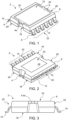
- FIG. 1 a perspective view of a semiconductor package 2 according to an embodiment of the invention is provided.
- the semiconductor package 2 is for a printed circuit board (PCB) insofar as it is attachable to a PCB to form part of an electrical circuit in operation.
- the semiconductor package 2 is of the form of a transistor.
- the semiconductor package 2 comprises a die paddle 4, a plurality of leads 6 and an encapsulant 8.
- the semiconductor package 2 comprises further components, obscured from view in Figure 1 , which will be described in detail later on in this document.
- the die paddle 4 is preferably manufactured from copper or a copper alloy, but other electronically conductive materials may otherwise be used.
- the die paddle 4 is a generally plate-like component, and is generally quadrangular.
- the die paddle 4 may be considered to form a base of sorts, in the manufacture of the semiconductor package 2, insofar as internal components of the semiconductor package 2 are built up on the die paddle 4.
- the die paddle 4 comprises first and second tabs 4a, 4b by which the die paddle 4 is connected to, and subsequently removed from, a lead frame during the manufacturing process (see Figures 11 a-i ).
- the reference numeral 6 generally denotes all of the leads.
- the leads 6 are for attachment of the semiconductor package 2 to a PCB.
- the leads 6 there are three types of leads. Firstly, there is a gate lead 10 (e.g. a switching lead). Secondly, there are a plurality of source leads 12 (not visible in Figure 1 but shown in Figure 2 ). Finally, there are a plurality of drain leads 14. Of note, whilst there is only a single gate lead 10, there are a plurality of source leads 12 and a plurality of drain leads 14. For the semiconductor package 2 shown in Figure 1 , the gate lead 10 is on the same side of the semiconductor package 2 as the source leads 12. The drain leads 14 are disposed on the opposing side of the semiconductor package 2.
- a gate lead 10 e.g. a switching lead
- source leads 12 not visible in Figure 1 but shown in Figure 2
- drain leads 14 there are a plurality of drain leads 14.
- the gate lead 10 is on the same side of the semiconductor package 2 as the source leads 12.
- the drain leads 14 are disposed on the opposing side of the semiconductor package 2.
- All of the leads 6 are in the form of gullwing leads insofar as there is a change of direction along their extent (e.g. there is an angular change of direction).
- the specific function of the leads will not be described in detail here.
- the gate, source and drain leads operate in a manner which is known to the person skilled in the art of semiconductor packages.
- encapsulant 8 may otherwise be described as a casing.
- the encapsulant 8 at least partly surrounds a die which (e.g. an internal component of the semiconductor package 2, which will be described in detail below) and provides a protective functionality.
- a die e.g. an internal component of the semiconductor package 2, which will be described in detail below
- the internal components of the semiconductor package 2, along with the allocation and position of the leads, will be shown and described in connection with Figures 11a-i which schematically illustrate a method of manufacturing the semiconductor package 2.
- the semiconductor package 2 shown in Figure 1 may be referred to as a top-cooled semiconductor package. This is owing to the fact that a surface of the die paddle 4, which may be referred to as a thermal pad, is exposed at a top side of the package. Put another way, the die paddle 4 is at least partly exposed at a top side of the semiconductor package 2.
- an underside, or first major face, of the semiconductor package 2 is labelled 16, whilst a top side, or second major face, is labelled 18.
- First and second sides of the semiconductor package 2, from which the gate and source leads 10, 12, and drain leads 14, respectively extend are labelled 20, 22.
- First and second ends of the semiconductor package 2, extending between the first and second sides 20, 22, are labelled 24, 26 respectively.
- the encapsulant 8 only extends across part of the second major face 18 of the semiconductor package 2. A region not covered by the encapsulant 8 leaves part of the die paddle 4 exposed, which provides a cooling functionality (e.g. a heat sink).
- a cooling functionality e.g. a heat sink
- Figure 2 an alternative perspective view of the semiconductor package 2 is provided. Whereas Figure 1 is taken generally from the perspective of the first major face 18, the perspective of Figure 2 is taken from the second major face 18. As such, features which were not visible in Figure 1 can be seen in Figure 2 .
- the bottom side, or underside, of the semiconductor package 2 (e.g. the first major face 16), shown in Figure 2 , is the side which is attached to a PCB in use.
- the gate lead 10 and the source leads 12 extending along the first side 20 are visible.
- the drain leads 14 extending along the second side 22 are also visible.
- an anchor pad 28 is visible.
- the anchor pad 28 is for attachment to the PCB. That is to say, the anchor pad 28 is another feature, as well as the leads 10, 12, 14, by which the semiconductor package 2 can be secured to a PCB. Incorporation of the anchor pad 28 is particularly advantageous because, particularly in applications where the semiconductor package 2 is a top-cooled arrangement (e.g. like in the present case) the various leads 10, 12, 14 by which the semiconductor package 2 is attached to the PCB may be subjected to stresses at such a level that the solder joint reliability is not met. Similarly, the solder joint pads, by which the leads are connected to the PCB, may be subjected to excessively high stresses. This can result in the semiconductor package 2 failing to meet solder joint reliability requirements (e.g. not being sufficiently robustly attached to the PCB).
- the anchor pad 28 by incorporating the anchor pad 28, the surface area by which the semiconductor package 2 is attached to the PCB is greatly increased. This, in turn, reduces the stresses induced in the leads 10, 12, 14 and the associated solder pads at the feet thereof. The thermal fatigue performance of the semiconductor package 2 is thus improved as a result, particularly for the gate lead.
- the anchor pad 28 can also advantageously provide a heatsink functionality in dissipating heat from the semiconductor package 2 by conduction.
- the anchor pad 28 extends across at least part of a die (not visible in Figure 2 but will be described in detail later). Furthermore, the anchor pad 28 is contained within a footprint defined by the encapsulant 8. Described another way, advantageously the anchor pad 28 does not extend beyond the encapsulant 8, which means the overall size of the semiconductor package 2 is not increased. The anchor pad 28 also does not extend beyond points at which leads 10, 12, 14 project from the encapsulant. As will be appreciated from Figure 2 , the anchor pad 28 is not covered by the encapsulant 8. As such, the anchor pad 28 remains exposed even after a moulding process, in which the encapsulant 8 (generally a polymer, such as plastic) is moulded to form the semiconductor package 2. See also Figures 11e and 11f , which will be described in detail below.
- the encapsulant 8 generally a polymer, such as plastic
- the anchor pad 28 is a solid body of material (e.g. does not incorporate an aperture) and also has a substantially rectangular outer perimeter. Similarly, anchor pad 28 extends across a majority of the die. However, these are all optional features.
- the anchor pad 28 forms part of an offset support 30.
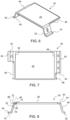
- the offset support 30 is also shown in alternative views in Figures 4 to 8 , including in isolation in Figures 6 to 8 , and further detail will be provided in connection with these figures.
- the anchor pad 28 is coupled to a drain terminal, and is specifically electrically connected to a drain terminal.
- the anchor pad 28 thus forms part of the electrical circuit of the semiconductor package 2.
- this is not essential, and the mere presence of the anchor pad 28, even if not electrically connected to the drain terminal, still provides advantages in more securely retaining the semiconductor package 2 on a PCB.
- FIG. 3 an end view of the semiconductor package 2 is provided taken generally from the first end 24.
- Figure 3 shows the first tab 4a of the die paddle 4, the encapsulant 8, and the gate and drain leads 10, 14 are shown extending through/projecting from the encapsulant 8.
- the anchor pad 24 is not visible from the end view shown in Figure 3 .
- FIG. 4 a perspective view of the semiconductor package 2 is provided with the encapsulant 8 omitted.
- first and second legs 32, 40 of the offset support 30 is visible.
- the legs 32, 40 may otherwise be described as projections.
- the first leg 32 is disposed proximate a first end 24 of the semiconductor package 2.
- the first leg 32 comprises a corresponding foot 34 (not visible in Figure 4 ) by which the leg 32, and anchor pad 28 and offset support 30 more generally, are coupled to the die paddle 4.
- the foot may otherwise be described as an attachment portion.
- the foot is substantially parallel to the anchor pad 28. This is also shown in connection with Figure 5 .
- first leg 32 only extends along part of a corresponding first edge 36 of the anchor pad 34. Rather, a clearance 38 is provided, along the first edge 36, along which the leg 32 does not extend, to allow space for the connector beneath.
- the second leg 40 is disposed proximate the second end 26 of the semiconductor package 2.
- the second leg 40 comprises a corresponding foot 42 by which the leg 40, and anchor pad 28 and offset support 30 more generally, are coupled to the die paddle 4.
- the foot may otherwise be described as an attachment portion.
- the foot 42 is substantially parallel to the anchor pad 28. This is also shown in connection with Figure 5 .
- the second leg 40 also only extends along part of the corresponding second edge 44 of the anchor pad 28.
- a clearance 46 is provided, along the second edge 44, along which the leg 40 does not extend, to allow space for the connector beneath.
- the anchor pad 28 is preferably distributed symmetrically between the first and second sides 20, 22 of the semiconductor package. This is owing to the presence of the leads disposed along each side of the semiconductor package.
- FIG. 5 an end view of the semiconductor package 2 is provided with the encapsulant 8 shown in a partially transparent state with the leads 6 omitted and generally from the first side 20 as labelled on Figures 4 and 2 .
- the second leg 40 is comparatively wider, in a lengthways direction, than the first leg 32.
- FIG. 5 a side view of the semiconductor package 2 is provided, and the encapsulant 8 is further provided in a partially transparent view.
- First and second major faces 16, 18 of the semiconductor package 2 are schematically indicated in Figure 5 .
- the orientation of the semiconductor package 2 in Figure 5 thus corresponds to that shown in Figure 2 .
- the first and second legs 32, 40 are shown extending from the anchor pad 28. Furthermore, respective feet 34, 42 are also shown, disposed at ends of the legs 32, 40. Respective solder pads 48, 50, between the die paddle 4 and the first foot 34 and second foot 42 respectively are also shown. By virtue of the solder pads 48, 50, the offset support 30 is attached to the die paddle 4.
- Figure 5 also demonstrates that the legs 32, 40 of the offset support 30 comprise a substantially perpendicular bend 52, 54.
- the (larger) angle defined between the anchor pad 28 and the legs 32, 40, corresponding to the first and second bends 52, 54, is approximately 110° in the illustrated embodiment.
- Substantially perpendicular bend is intended to include any complimentary angle pairing where the larger angle is between around 60° and around 120°.
- the legs may comprise a perpendicular bend insofar as the bend is equal to 90°. More detail regarding the angles is provided in connection with Figure 8 .
- Figure 5 also shows die 56, the die 56 being coupled to the die paddle 4.
- a corresponding (first) solder pad which couples the die 56 to the die paddle 4 is labelled 58.
- a (fifth) solder pad is labelled 60.
- a connector 90 is coupled to the die 56 via the solder pad 60.
- the connector 90 comprises a plurality of leads for attachment to the PCB.
- the portion of the connector 90 visible in Figure 5 corresponds comprises the gate and source leads 10, 12 (although neither of which is visible in Figure 5 ).
- the semiconductor package 2 comprising the two legs 32, 40 extending from opposing sides of the anchor pad 28 improves the robustness of the coupling between the anchor pad 28 and the die paddle 4.
- the anchor pad 28 is attached to the PCB, the overall robustness of the attachment of the semiconductor package 2 to the PCB (via the anchor pad 28 and associated feet of each of the gate, source and leads 10, 12, 14) is improved as a result.
- the offset support 30 comprises anchor pad 28 and first and second feet 32, 40 which extend from first and second edges 36, 44 of the anchor pad 28.
- Each of the first and second legs 32, 40 comprises a respective foot 34, 42 at an end thereof, by which the respective leg, and offset support 30 generally, are attached to the PCB.
- Each of the first and second legs 32, 40 further comprises one or more apertures provided therein.
- the apertures advantageously improve the flow of mould material (i.e. of the encapsulant 8) and provide mould locking features (which reduce the risk of delamination). The apertures thus improve the manufacture, and robustness of, the encapsulant 8.
- FIG. 7 a plan view of the offset support 30 is provided.
- the plan view thus shows each of the first and second legs, 32, 40 extending from the anchor pad 28.
- the clearances 38, 46 provided at each of the first and second edges 36, 44 of the anchor pad 28 are also visible.
- differing lengthways extents of the first and second legs 34 to 40 are shown in Figure 7 .
- Figure 7 also shows the first leg 32 comprising one aperture, whereas the second leg 40 comprises three (e.g. a plurality of) apertures.
- the apertures take the form of lozenge-shaped (e.g. oval) apertures, but other geometries could otherwise be used.
- Figure 8 a side view of the offset support 30 is provided.
- Figure 8 therefore provides a similar view of the offset support 30 to that shown in Figure 5 , but with other features of the semiconductor package omitted.
- first plane 66 Schematically annotated on Figure 8 is a first plane 66 extending through a midpoint of a thickness at the anchor pad 28. Also labelled is a second plane 68 which extends through a midpoint of a thickness of the first leg 32, and a third plane 70 which extends through a midpoint of a thickness of the second leg 40. Each of the first, second and third planes is thus indicative of a direction of each of the anchor pad 28, first leg 32 and second leg 40 extend in.
- First and second complimentary angles 72, 74 are schematically annotated between the first plane 66 and the second plane 68. As will be appreciated from Figure 8 , in the illustrated embodiment the first angle 72 is larger than the second angle 74.
- the bend 52 is a substantially perpendicular bend.
- a substantially perpendicular bend is intended to mean that a larger of the first and second complimentary angles 72, 74 falls within the range 60 degrees to 120 degrees. Any angle falling outside of this range would mean that the bend is no longer substantially perpendicular. It will be appreciated that in some embodiments the bend may be a perpendicular bend, in which case the angle 72, 74 would be equal to 90 degrees. By way of an example, the first angle 72 may be between 90 and 120 degrees, and the second angle 74 may be between 60 and 90 degrees.
- first and third planes 66, 70 are substantially parallel to one another. This is intended to mean that an angular offset between the planes 66, 70 is less than around 5 degrees.
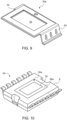
- FIG 9 a perspective view of an offset support 30a according to another embodiment is provided.
- the offset support 30a shares many features in common with the offset support 30 described and shown in connection with Figures 4-8 . As such, for brevity common features will not be described again in detail.
- the offset support 30a comprises first and second legs 32, 40 and an anchor pad 28a.
- a primary difference between the offset support 30a and the offset support 30 is that the anchor pad 28a comprises an aperture 76.
- the aperture 76 is a centrally located rectangular aperture.
- the pad 28a is not a solid body of material, but instead comprises the aperture 76.
- the anchor pad 28a thus takes the form of generally rectangular annulus.
- the anchor pad 28a may otherwise be described as having a thickness or border, which extends around the aperture 76.
- an advantage of the support 30a is that the aperture 76 provides an inspection window through which the alignment of other components forming part of a semiconductor package incorporating the offset support 30a can be assessed. Incorporation of the aperture 76 means that an inspection window can be used while still providing all of the other associated advantages of the anchor pad 28 (e.g. improving the robustness of the connection of the semiconductor package to the PCB).
- the alignment of the gate clip (94 - visible in Figure 11d ) is sensitive with respect to the die, and it is desirable to be able to inspect this alignment via the aperture 76.
- FIG 10 a perspective view, generally of an underside of a semiconductor package 2a according to another embodiment is provided.
- the semiconductor package 2a incorporates the offset support 30a, but otherwise shares many features in common with the semiconductor package 2 shown and described in connection with Figures 1-3 .
- the view shown in Figure 10 , of the semiconductor package 2a is very similar to that shown in Figure 2 , save for the differences associated with the anchor pad 28 (28a). Accordingly, for brevity the description which is common to both embodiments will not be repeated here, and only the differences will be described in detail.
- the underside (e.g. first major side) of the semiconductor package 2a comprises the anchor pad 28a.
- a portion 78 of the encapsulant 8 also extends within the anchor pad 28a. Described another way, the aperture 76 as shown in Figure 9 is effectively filled with, or covered by, the encapsulant 8. This defines the portion 78 of encapsulant which fills the aperture. This portion 78 may be said to cap the aperture 76.
- the portion 78 of encapsulant 8 still protects the internal components of the semiconductor package 2a in the normal way that an encapsulant 8 would.
- this functionality is advantageously provided in combination with the fact that: i) the anchor pad is incorporated; and ii) inspections of the internal components of the semiconductor package 2a can be more readily conducted as part of the assembly and verification process.
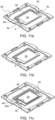
- FIGS 11a-11i a method of manufacturing a semiconductor package, corresponding to the semiconductor package 2a shown in Figure 10 , is schematically illustrated. The method may otherwise be described as a process flow.
- a lead frame 80 is shown, in a perspective plan view.
- the lead frame 80 is effectively a sheet of material, with material having been selectively removed, such as by stamping or etching, in order to define one or more die paddles (only one being shown in Figure 11a , and labelled 4).
- the lead frame 80 may otherwise be described as a common lead frame (e.g. in embodiments where the lead frame 80 defines a plurality of die paddles).
- Figure 11a also shows the die paddle 4 being attached to the lead frame 80 by first and second tabs 4a, 4b.
- first and second tabs 4a, 4b are severed, or cut, to detach the die paddle 4, and association semiconductor package, from the lead frame 80.
- Figure 11a shows a manufacturing step beyond the lead frame 80 in isolation.
- solder has been printed onto the die paddle 4, in multiple locations, in advance of the coupling of further features to the die paddle 4.
- a first (die) pad 58 occupies most of the surface area of the die paddle 4.
- a second (drain) pad 84 is also printed along one side of the die paddle 4.
- the second pad 84 is elongate, and may be described as strip-like.
- the drain pad 84 is the solder pad to which a drain clip 92 (e.g. part of the connector 90) is coupled.
- third and fourth pads 48, 50 are also printed, generally at either end of the second pad 84.
- the third and fourth pads 48, 50 are smaller than the second pad in surface area. In the illustrated embodiment the third pad 48 is also smaller than the fourth pad 50. As shown in Figure 11e , the third and fourth pads 48, 50 are the locations which correspond to the first and second feet 34, 42 of the offset support 30a (see also Figure 5 ). As such, the offset support 30a is coupled to the die paddle 4 via the third and fourth pads 48, 50.
- the step shown in Figure 11a may be described as a solder layer being printed on the, or each, die paddle.
- the solder layer may be applied by a screen printing process.
- the solder layer may be described as being dispensed or applied to the die paddle 4.
- the solder layer is preferably applied to all of the die paddles (if appropriate) in this single process step.
- Figure 11b shows a further step in which the die 56 is coupled to the die paddle 4.
- the die 56 which comprises a semiconductor material, is placed onto the first pad 58. Coupling the die 56 may be described as the die 56 being placed onto the solder layer 58. As described above, the solder layer 58 is in turn, disposed on the die paddle 4.
- each of a plurality of die paddles is provided with a die.
- the second to fourth pads 84, 48, 50 are still exposed in this step, and the die 56 is not attached to these pads. Second to fourth pads 84, 48, 50 are thus still available, or 'vacant', following attachment of the die 56.
- solder layer 64 may otherwise be described as being printed onto, or applied to, the die 64.
- solder is applied to each die (for a leadframe comprising a plurality of die paddles).
- the solder layer 64 is preferably applied to all of the dies in this single process step.
- the solder layer is preferably applied to all of the dies simultaneously.
- the solder layer may be applied to the dies in a consecutive manner (e.g. die by die).
- the solder layer 64 may be described as a fifth pad.
- the second to fourth pads 84, 48, 50 are still exposed in this step, and the die 56 is not attached to these pads. Second to fourth pads 84, 48, 50 are thus still available, or 'vacant', following attachment of the die 56.
- a connector 90 is coupled to the subassembly.
- the connector 90 comprises a drain clip 92, a gate clip 94 and a source clip 96 in the illustrated embodiment.
- the drain clip 92 is separate from the gate and source clips 94, 96.
- the connector 90 may be described as a multi-part connector comprising a first part (e.g. the drain clip 92) and a second part (e.g. the conjoined gate and source clips 94, 96).
- the gate and source clips 94, 96 are in a conjoined state in Figure 11d , but are separated from one another in a subsequent step.
- the drain clip 92 is coupled to the die paddle 4 via the second pad 84 (see Figures 11a-c ).
- the gate clip 94 portion of the conjoined clip is coupled to the die 56 via an exposed portion of the die 56 labelled 56a in Figure 11c .
- the source clip 96 portion of the conjoined clip is coupled to the die 56 via the fifth pad 64 (see Figure 11c ).
- Projections extending from each of the clips 92, 94, 96 as shown in Figure 11d define the leads 10, 12, 14 as shown in Figures 11h and 11i .
- Third and fourth pads 48, 50 are still exposed, or ⁇ vacant', following attachment of the drain clip 92 in this embodiment.
- FIG. 11e a step of the manufacturing process is shown in which the offset support 30a is attached.
- the offset support 30a is coupled to the die paddle 4 via the third and fourth pads 48, 50 (not labelled in Figure 11e , but see Figure 11d ).
- first and second feet 34, 42 (42 not visible in Figure 11e ) of the first and second legs 32, 40 are placed onto third and fourth pads 48, 50 on the die paddle 4.
- the offset support 30a is thus attached to the subassembly.
- the aperture 76 provides a window through which the source clip 96 alignment, and indeed alignment of other ⁇ internal' components of the subassembly can be observed.
- the anchor pad 28a extends across a majority of the die 56, and may be described as extending over, and across, the source clip 96.
- the anchor pad 28a is also vertically offset from the die paddle 4 by virtue of the legs 32, 40 of the offset support 30a. As shown in Figure 11e , it is desirable that the anchor pad 28a does not overlap the gate clip 94. This is for at least the reason that the alignment of the gate clip 94 is particularly sensitive with respect to the die 56. Furthermore, this reduces the risk of exposed copper after moulding the encapsulant.
- FIG. 11f a moulding step of the process is shown.
- encapsulant 8 is moulded over the die 56 (and various other components).
- the moulding process occurs by way of injection moulding.
- the mould/mould cavity is not shown in Figure 11f .
- the anchor pad 28a remains visible, or exposed, even after moulding occurs. Accordingly, the aperture 76 through the anchor pad 28a, as shown in Figure 11e , is 'filled' with the moulded material such that the portion 78 of encapsulant is defined.
- FIG 11g a deflash and plating step is shown.
- exposed copper features such as projections of the various clips, the anchor pad 28a etc. are plated to improve robustness and reduce the risk of corrosion in this step.
- the plating also improves the adherence of solder to the leads.
- the leadframe 80 more generally, is also plated.
- the components are generally plated with Tin (Sn).
- FIG 11h shows a step of the process after a trim, form and singulation (TFS) step has occurred.
- TFS is a (multi-stage) punching process in which dambars between leads are removed, the leads are defined, and the leads are then formed (into gullwing [e.g. displaced] leads).
- TFS also singulates the semiconductor package 2a (e.g. separates it from the surrounding leadframe 80 of the preceding Figures).
- the gate lead 10, source leads 12 and drain leads 14 are labelled in Figure 11h .
- Figure 11i shows the semiconductor package 2a from an underside perspective view.
- the anchor pad 28a remains exposed (albeit plated). Furthermore, the anchor pad 28a lies in the same plane as feet of the various leads.
- one or more reflow steps in which the solder layers, applied in steps shown in Figures 11a and 11c , undergo a reflow soldering process may occur.
- the semiconductor package 2a, or subassembly thereof ma be subjected to a controlled elevated temperature, such as being passed through a reflow oven or passed under an infrared lamp, to create permanent soldered joints to 'cure' the semiconductor package 2a.
- FIG. 12 to 14 two perspective, and one end, views of a semiconductor package 102 according to another embodiment are provided. Given the near identical nature of the semiconductor package 102 shown in Figures 12-14 to the semiconductor package 2 shown in Figures 1-3 , no further description will be provided in connection with these Figures. The description in connection with Figures 1-3 applies equally here.
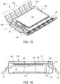
- FIG. 15 perspective view of the semiconductor package 102 with an encapsulant 8 omitted is shown.
- the view shown in Figure 15 shows the die paddle 4, a die 56 coupled to the die paddle and gate and source clips 94, 96 coupled to the die 56.
- the semiconductor package 102 comprises anchor pad 28.
- the anchor pad 28 forms part of an integral drain clip and offset support 130.
- the integral drain clip and offset support 130 also provides the functionality of a drain clip.
- the integral support 130 also comprises a plurality of leads 110 which define drain leads of the semiconductor package 102.
- the plurality of leads 110 are specifically displaced leads (e.g. gullwing leads).
- a further distinction of the anchor pad 28 lies in the way in which it is coupled to the semiconductor package 102.
- first and second legs extended from opposing edges of the anchor pad 28, the integral support and drain clip 130 takes the form of a cantilever. That is to say, in the embodiments shown in Figure 15 , a single leg 106 extends from an edge 108 of the anchor pad 28. As such, the anchor pad 28 is supported entirely by the one leg 106. However, additional legs could otherwise be incorporated.
- the plurality of legs extend from short sides of the anchor pad, in this embodiment the leg 106 extends from a single long edge 108 of the anchor pad 28.
- the anchor pad 28 is electrically connected, and coupled to, a drain terminal (e.g. drain pad) of the semiconductor package 102.
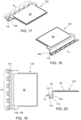
- FIG 16 an end view of the semiconductor package 102 is provided. Furthermore, the encapsulant 8 is shown in a partially transparent view.
- Figure 16 shares many features in common with that shown in Figure 5 (other than for being in a reversed orientation).
- the die 56 is coupled to the die paddle 4 by a first die solder pad 58.
- the gate lead 10 is defined by gate clip 94, the gate clip 94 being coupled to the die 56.
- Figure 16 shows the leg 106 of the integral clip and support 130 extending at a perpendicular angle to the anchor pad 28. Furthermore, a U-shaped portion 110 at an end of the leg 106 defines a foot by which the integral clip and support 130 is coupled to the die paddle 4. The drain lead(s) 14 extend from the U-shaped portion 110.
- the integral clip and offset support 130 takes the form of a cantilever in which the single leg 106 extends from the drain pad 28, specifically a long edge 108 thereof, at a perpendicular angle.
- a U-shaped portion 110 defines a foot by which the integral support 130 is attachable to a semiconductor package. Extending from the opposing side of the U-shaped portion 110 are a plurality of drain leads 14. The drain leads 14 define a drain clip of the semiconductor package.
- the anchor pad 28 takes the form of a solid body of material in that there is no aperture through the anchor pad 28.
- an aperture e.g. 76 as shown in connection with Figure 9
- the anchor pad 28 has a rectangular outer perimeter and also extends across a majority of the die.
- the leg 106 comprises three perpendicular bends: a first bend 52 adjacent the anchor pad 28, a second bend 112 provided at a first end of the U-shaped portion 110 and a third bend 114 provided at an opposing end of the U-shaped portion 110.
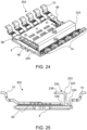
- FIG. 21a-i a method of manufacturing the semiconductor package 102 is schematically indicated.
- these method steps share many details and features in common with Figures 11a-i , as described in connection with the semiconductor package 2a, which will not be repeated here for brevity. Instead, only the differences will be described in detail.
- FIG. 21d this is the first method step which deviates slightly from corresponding step shown in Figure 11d .
- a connector 190 is coupled to the subassembly (i.e. specifically coupled to the die paddle 4).
- the connector 190 does not comprise a drain clip.
- the connector 190 comprises only a gate clip 94 and a source clip 96.
- the gate and source clips 94, 96 are in a conjoined state in Figure 21d , and are separated from one another in a subsequent step.
- the connector 190 is a single-piece connector as attached in Figure 21d .
- the second pad 84 is still exposed after the connector 190 has been attached.
- FIG. 21e a step is shown in which the integral drain clip and offset support 130 is attached (e.g. to the die paddle 4).
- the integral drain clip and offset support 130 is coupled to the die paddle 4 by the second pad 84 (not visible in Figure 21e but shown in Figure 21d ).
- the U-shaped portion 110 of the leg 106 contacts the second pad 84.
- the drain clip 92 is thus incorporated in the integral offset support 130.
- the anchor pad 28 extends across, and over, the gate and source clips 94, 96.
- the connector 190 and integral drain clip and support 130 may be attached simultaneously.
- the anchor pad 28 preferably overlaps the gate clip 96 (and so connector 190), at least partly, it is preferred that the integral drain clip and offset support 130 be coupled to the die paddle 4 after the connector 190 has been coupled to the die paddle 4.
- FIG. 21f like that described in connection with Figure 11f a moulding step is shown in which an encapsulant 8 is moulded at least partly over the die and various other components of the semiconductor package 102. Owing to the geometry of the mould (not shown in Figure 21f ), the anchor pad 28 remains exposed even after moulding (i.e. the encapsulant does not cover the anchor pad 28).
- Figures 21g-i correspond generally to steps Figure 11g-i , and will therefore not be described in detail. That said, in the finalised, singulated semiconductor package 102 shown in Figures 21h and 21i , the finished product is identical to that shown for the semiconductor package 2a of Figures 11h and 11i , save for the aperture in anchor pad 28a.
- Providing the integral offset support and drain clip 130 is advantageous for a number of reasons.
- the efficiency of manufacturing can be improved by virtue of combining the anchor pad 28 with the drain clip.
- the anchor pad only be incorporated with the drain clip, as opposed to the gate and or source clips, because incorporating the anchor pad as part of the source clip can be found to increase the RDS of the package (e.g. resistance) and reduce the performance accordingly.
- FIG 22 a perspective view of a semiconductor package 202 according to another embodiment is provided, with an encapsulant omitted.
- the semiconductor package 202 shows many features in common with the semiconductor package 102 shown and described in connection with Figures 12 to 16 . Much of the previous description therefore also applies here, and only the differences will be described in detail.
- the semiconductor package 202 comprises an integral drain clip and offset support 230.
- the integral drain clip and offset support 230 comprises an anchor pad 228 which is formed of a solid body of material (but could incorporate an aperture in some embodiments).
- the anchor pad 228 extends across at least part of the die 56.
- the anchor pad 228 is comparatively smaller and extends across only part of the die 56 (i.e. as opposed to extending across a majority of the die 56).
- a leg 232 which extends from the anchor pad 228 does not comprise a substantially perpendicular bend. Instead, the leg 232 extends at a shallower angle (e.g. 45 to 60 degrees).
- the semiconductor package 202 otherwise shares many features in common with the earlier embodiments.
- a slight height difference is shown between the anchor pad 228 and pads of the gate and drain 10, 14. This may be achieved by grinding the encapsulant to expose the anchor pad 228.
- Figure 24 is a perspective view of a further embodiment of semiconductor package 302.
- Semiconductor package 302 shares various features in common with the semiconductor package 302 shown in Figures 22 and 23 and the semiconductor package 102 shown in Figures 12-16 . Much of the previous description therefore applies equally, and only the differences will be described in detail.
- the semiconductor package 302 comprises an integral drain clip and offset support 330.
- the integral drain clip and offset support 330 comprises an anchor pad 328 which extends across at least part of the die 56. Furthermore, a leg 332 extends from the anchor pad 328. The leg 332 comprises a substantially perpendicular bend 333 proximate the anchor pad 328. A U-shaped portion 334 is disposed at the other end of the leg 332. The U-shaped portion defines an attachment portion by which the integral clip and offset support 330 is attachable to the die paddle 4.
- the anchor pad 328 does not extend across a majority of the die 56, but instead extends across only part of it (e.g. less than around 50% of the surface area of the die, more preferably less than around 30%). Owing to the single leg 332, the integral offset support 330 also has a cantilever design. The anchor pad 328 extends along an entire long edge 336 of the die 56.
- any bend defined by the offset support or integral drain clip and offset support may comprise one or more apertures.
- the apertures may be through-holes.
- the apertures facilitate the forming of the bend when the component is manufactured.
- the offset support, and integral drain clip and offset support is preferably manufactured from copper or a copper alloy.
- the offset support, and integral drain clip and offset support is preferably manufactured using a stamping or forming process.
Landscapes
- Lead Frames For Integrated Circuits (AREA)
- Physics & Mathematics (AREA)
- Geometry (AREA)
- Engineering & Computer Science (AREA)
- Microelectronics & Electronic Packaging (AREA)
Abstract
There is disclosed a semiconductor package for a PCB. The semiconductor package comprises a die paddle, a die, a connector, an anchor pad and an encapsulant. The die is coupled to the die paddle. The connector is coupled to the die, the connector comprising a plurality of leads for attachment to the PCB. The anchor pad is for attachment to the PCB. The encapsulant at least partly surrounds the die. The anchor pad extends across at least part of the die.
Description
- The present invention relates to a semiconductor package for a PCB, a method of manufacturing the semiconductor package, a method of attaching the semiconductor package to a PCB, an offset support for a semiconductor package, and an integral drain clip and offset support for a semiconductor package.
- Semiconductor packages, such as transistors, are manufactured as layered assemblies including components such as die paddles, dies, connectors and an encapsulant (e.g. casing). Semiconductor packages are attached to a Printed Circuit Board (PCB) by coupling leads of the connector, of the semiconductor package, to the PCB (e.g. using solder).
- Semiconductor packages are typically only attached to the PCB via the leads of the connector. The soldered joints, between the leads and the PCB, and the leads themselves, may be subjected to thermal fatigue cycles, and associated plastic strain, in operation, and can be susceptible to failure if not sufficiently robust.
- There exists a need to overcome the disadvantages associated with existing semiconductor assemblies, and associated methods of manufacture, whether mentioned in this document or otherwise.
- According to a first aspect of the invention there is provided a semiconductor package for a PCB, comprising:
- a die paddle;
- a die coupled to the die paddle;
- a connector coupled to the die, the connector comprising a plurality of leads for attachment to the PCB;
- an anchor pad for attachment to the PCB; and
- an encapsulant which at least partly surrounds the die; wherein
- the anchor pad extends across at least part of the die.
- The semiconductor package may be a transistor. The semiconductor package may take the form of a dual-in-line (DIL) package (e.g. having two rows of leads, each row occupying a different opposed side of the package).
- The die paddle may otherwise be described as a plate of conductive material. The die paddle may be manufactured from a copper alloy or entirely from copper.
- The die may be a single component or may comprise multiple constituent components. The die is preferably coupled to the die paddle using solder. The die being coupled to the die paddle may otherwise be described as the die being attached to the die paddle. The die may be a silicon chip. One die may be coupled to each die paddle.
- The connector may comprise a clip. The connector may be wirebonded to the die, or coupled using any other internal connection (e.g. a ribbon band). The clip may comprise one or more leads. The connector (e.g. clip) may be described as a conductive body by which the semiconductor package is connected, or connectable, to an external electrical circuit in use. The connector (e.g. clip) may be coupled to the die paddle by virtue of being coupled to the die. Described another way, the connector may be described as being indirectly coupled to the die paddle. The clip is preferably coupled to the die by solder. The connector may be a multi-part connector. For example, the connector may comprise a drain clip, gate clip and source clip (e.g. a plurality of clips). In some embodiments the connector may not comprise the drain clip. The gate clip and source clip (for example) may be conjoined to one another when that portion of the connector is first coupled to the die. The gate and source clip may be separated during a trim, form and singulate (TFS) step of the manufacture process. In preferred embodiments, there is a single gate lead, and a plurality of source and drain leads. There is preferably one more drain lead than there is gate lead (the gate lead and source leads preferably being disposed along one side of the semiconductor package).
- The plurality of leads may be displaced leads (e.g. gullwing leads, incorporating a change of direction along their extent). Displaced leads have advantageously been found to provide improved board level reliability by acting as a stress reliever when the semiconductor package is installed in an electrical circuit. The `leads' may otherwise be described as projections (e.g. projecting beyond the encapsulant). Each lead may define a respective foot.
- The anchor pad may form part of an offset support. Alternatively, the anchor pad may form part of an integral drain clip and offset support. The anchor pad is preferably coupled to the die paddle (e.g. via solder). The anchor pad may be coupled to, and offset from, the die paddle. The anchor paddle is preferably attachable to the die paddle by one or more legs which extend from the anchor pad. The anchor pad is distinct from the plurality of leads of the connector for at least the following reasons. Firstly, the anchor pad has a comparatively larger surface area than each of the feet of the leads. The anchor pad also preferably lies within a footprint of the encapsulant. Described another way, unlike the plurality of leads, which at least partly extend beyond a footprint of the encapsulant (e.g. and therefore project therefrom), the anchor pad does not project from, or beyond, the encapsulant. The anchor pad therefore does not increase the overall size of the semiconductor package. The anchor pad also preferably occupies a central region of the semiconductor package in at least some embodiments. Put another way, the encapsulant extends around each of the sides of the anchor pad. In preferred embodiments the anchor pad extends across the majority of the die (e.g. over at least around 70% of the die by surface area). The anchor pad is preferably plated in a similar manner to the feet of the plurality of leads.
- The encapsulant may otherwise be described as a casing or shield. The encapsulant may be described as encasing the die. The encapsulant advantageously reduces the risk of contaminants, such as moisture, penetrating into the semiconductor package. The encapsulant preferably extends between first and second major faces of the die paddle (however, at least one major face of the die paddle may remain exposed [e.g. as a thermal pad, as a heatsink]). The encapsulant may be plastic. The encapsulant may otherwise be described as being manufactured from a polymer. The encapsulant is preferably manufactured using an injection moulding process where an at least partially molten material is moulded into the desired encapsulant shape. The plastic may be a thermoplastic (e.g. a thermosetting polymer).
- Advantageously, the anchor pad provides another attachment point by which the semiconductor package can be secured to a PCB. In known arrangements, the semiconductor package is only attached to the PCB via a plurality of leads, specifically feet thereof. This has been found to increase the risk that the solder joints do not pass reliability tests, particularly for top-cooled embodiments (e.g. where the die paddle is provided proximate an upper surface of the semiconductor package in use [i.e. distal the leads]). By also attaching the semiconductor package to the PCB via the anchor pad, the robustness of the connection is improved and the semiconductor package is more reliably retained on the PCB.
- The anchor pad may be coupled to a drain terminal.
- The anchor pad being coupled to a drain terminal may otherwise be described as the anchor pad being coupled to a drain pad. The anchor pad may be described as being coupled to the die paddle via the drain terminal.
- The anchor pad may be electrically connected to the drain terminal.
- The anchor pad being electrically connected to the drain terminal may otherwise be described as the anchor pad being electrically connected to the drain paid. The anchor pad may be electrically connected to one or more drain pads. The anchor pad may be described as being in electrical communication with the drain terminal.
- Where the anchor pad is electrically connected to the drain terminal, the anchor pad can also be used to electrically connect the semiconductor package of a PCB in operation. Advantageously, the anchor pad thus forms part of the electrical circuit. However, in other embodiments the anchor pad may be either electrically isolated from the semiconductor package or attached to a PCB, but the PCB not having a corresponding terminal or connection for electrical communication with the anchor pad.
- The anchor pad may be a solid body of material.
- The anchor pad being a solid body of material may otherwise be described as the anchor pad being a continuous body of material. Put another way, the anchor pad does not incorporate any aperture or other recess. Advantageously, the anchor pad being a solid body of material provides a greater surface area by which the semiconductor package can be attached to a PCB.
- The anchor pad may comprise an aperture.
- The anchor pad comprising an aperture may otherwise be described as the anchor pad not being defined by a solid body of material. The anchor pad may comprise a single aperture or a plurality of apertures.
- Advantageously, the anchor pad comprising an aperture provides an inspection window through which other internal components of the semiconductor package (e.g. the die and/or connector) can be viewed. For example, by incorporation of the aperture an inspection window can be defined by which an operator can check the alignment of the connector with respect to the die. The aperture thus advantageously improves the quality control process.
- The anchor pad may have a substantially rectangular outer perimeter.
- Substantially rectangular outer perimeter is intended to refer to an outer perimeter which is generally defined by two pairs of parallel sides. Corners of the rectangular perimeter may be filleted, and this is still considered to define a substantially rectangular outer perimeter.
- The anchor pad may extend across a majority of the die.
- The anchor pad extending across a majority of the die advantageously means that there is a greater surface area available on the anchor pad for attachment of the semiconductor package to the PCB. An example of the anchor pad extending across a majority of the die is the anchor pad extending across at least 70% of a surface area of the die.
- One or more legs may extend from the anchor pad.
- The one or more legs of the anchor pad may comprise a plurality of legs. The one or more legs be described as extending from an edge of the anchor pad. One leg may extend from each of a plurality of edges of the anchor pad. The anchor pad may take the form of a cantilever arrangement (e.g. with a single leg extending from only one side of the anchor pad) or may take the form of a bridge in which multiple legs extend from opposing sides of the anchor pad.
- Advantageously, the one or more legs provide a feature by which the anchor pad can be offset from the die paddle. Described another way, the one or more legs can vertically offset the anchor pad from the die paddle. Advantageously, for a top-cooled embodiment where the die paddle is disposed proximate a top side of the semiconductor package, the anchor pad can thus be provided proximate the bottom side of the semiconductor package.
- Two legs may extend from opposing sides of the anchor pad.
- Two legs extending from opposing sides of the anchor pad may otherwise be described as a bridge embodiment. Advantageously, two legs extending from opposing sides of the anchor pad (e.g. one leg extending from each side) has been found to provide an improvement in the robustness of the connection of the anchor pad to the die paddle. An associated improvement of the robustness of the join between the semiconductor package and PCB more generally have been found to result. Each of the legs may be substantially identical. Alternatively, the legs or one or more legs may be different from one another. For example, one leg may be comparatively thinner in a lengthways direction than the other leg.
- The one or more legs may comprise a substantially perpendicular bend.
- One or more legs comprising a substantially perpendicular bend may comprise each of the plurality of legs comprising a substantially perpendicular bend. A perpendicular bend is intended to refer to a complimentary angle pair where the larger of the two angles falls within the
range 60 degrees to 120 degrees. - The substantially perpendicular bend may comprise a perpendicular bend (e.g. of 90 degrees).
- Incorporation of the substantially perpendicular bend has advantageously been found to improve the robustness of the attachment of the anchor pad to the semiconductor package.
- The anchor pad may be integral with a drain clip.
- The anchor pad being integrral with the drain clip may otherwise be described as the anchor pad forming part of an integral drain clip and offset support. The anchor pad being integral with the drain clip may be described as the anchor pad defining one or more drain leads.
- According to a second aspect of the invention there is provided a method of manufacturing the semiconductor package according to the first aspect of the invention, comprising:
- coupling the die to the die paddle;
- coupling the connector to the die;
- coupling the anchor pad to the die paddle; and
- moulding the encapsulant at least partly over the die.
- Coupling the connector to the die may comprise coupling a conjoined gate and source clip to the die.
- Coupling the anchor pad to the die paddle may comprise coupling an integral drain clip to the die paddle.
- According to a third aspect of the invention there is provided a method of attaching the semiconductor package according to the first aspect of the invention to the PCB, the method comprising:
- applying solder to the plurality of leads and the anchor pad or applying solder to a plurality of positions on the PCB; and
- coupling the plurality of leads and the anchor pad to the PCB to attach the semiconductor package to the PCB.
- Applying solder to the plurality of leads may otherwise be described as applying solder to corresponding feet of the plurality of leads. In some embodiments solder is applied to a plurality of positions on the PCB, and the semiconductor package (e.g. the feet of the leads and the anchor pad) then placed thereon.
- The method may further comprise a reflow step in which the solder is cured.
- According to a fourth aspect of the invention there is provided an offset support for a semiconductor package, comprising:
- an anchor pad for attachment to a PCB;
- one or more legs extending from the anchor pad, the one or more legs having an attachment portion, substantially parallel to the anchor pad, for attachment to a die paddle.
- According to a fifth aspect of the invention there is provided an integral drain clip and offset support for a semiconductor package, comprising:
- an anchor pad for attachment to a PCB;
- one or more legs extending from the anchor pad, the one or more legs having an attachment portion, substantially parallel to the anchor pad, for attachment to a die paddle; and
- one or more leads defining at least part of a drain clip of the semiconductor package.
- The optional and/or preferred features of each aspect of the invention as set out herein are also applicable to any other aspect of the invention where appropriate.
- Embodiments of the present invention will now be described, by way of example only, with reference to the accompanying drawings in which:
-
Figure 1 is a perspective view of a semiconductor package according to an embodiment of the invention; -
Figure 2 is an alternative perspective view of the semiconductor package ofFigure 1 ; -
Figure 3 is an end view of the semiconductor package ofFigures 1 and 2 ; -
Figure 4 is a perspective view of the semiconductor package ofFigures 1 to 3 with an encapsulant omitted; -
Figure 5 is a side view of the semiconductor package ofFigures 1 to 4 , with the encapsulant shown in a partially transparent view; -
Figure 6 is a perspective view of an offset support in accordance with an embodiment of the invention, the offset support forming part of the semiconductor package ofFigures 1 to 5 ; -
Figure 7 is a plan view of the offset support ofFigure 6 ; -
Figure 8 is a side view of the offset support ofFigures 6 and 7 ; -
Figure 9 is a perspective view of an offset support according to another embodiment of the invention; -
Figure 10 is a perspective view of a semiconductor package incorporating the offset support ofFigure 9 ; -
Figures 11a-i schematically illustrate a method of manufacturing the semiconductor package ofFigure 10 ; -
Figure 12 is a perspective view of a semiconductor package according to another embodiment of the invention; -
Figure 13 is an alternative perspective view of the semiconductor package ofFigure 12 ; -
Figure 14 is an end view semiconductor package ofFigures 12 and 13 ; -
Figure 15 is a perspective view of the semiconductor package ofFigures 12 to 14 with an encapsulant omitted; -
Figure 16 is an end view of the semiconductor package ofFigure 15 with the encapsulant shown in a partially transparent view; -
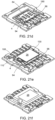
Figures 17 and 18 are alternative perspective views of an integral drain clip and offset support according to another embodiment, forming part of the semiconductor package ofFigures 12 to 16 ; -
Figure 19 is a plan view of the integral drain clip and offset support ofFigures 17 and 18 ; -
Figure 20 is an end view of the integral drain clip and offset support ofFigures 17 to 19 ; -
Figures 21a-i schematically illustrate a method of manufacturing the semiconductor package ofFigures 12 to 14 ; -
Figure 22 is a perspective view of a semiconductor package according to another embodiment with an encapsulant omitted; -
Figure 23 is an end view of the semiconductor package ofFigure 22 ; -
Figure 24 is a perspective view of a semiconductor assembly according to another embodiment of the invention with an encapsulant omitted; -
Figure 25 is an end view of the semiconductor package ofFigure 24 . - Turning to
Figure 1 , a perspective view of asemiconductor package 2 according to an embodiment of the invention is provided. Thesemiconductor package 2 is for a printed circuit board (PCB) insofar as it is attachable to a PCB to form part of an electrical circuit in operation. Thesemiconductor package 2 is of the form of a transistor. - As shown in
Figure 1 , thesemiconductor package 2 comprises adie paddle 4, a plurality ofleads 6 and anencapsulant 8. Thesemiconductor package 2 comprises further components, obscured from view inFigure 1 , which will be described in detail later on in this document. - Beginning with the
die paddle 4, thedie paddle 4 is preferably manufactured from copper or a copper alloy, but other electronically conductive materials may otherwise be used. Thedie paddle 4 is a generally plate-like component, and is generally quadrangular. Thedie paddle 4 may be considered to form a base of sorts, in the manufacture of thesemiconductor package 2, insofar as internal components of thesemiconductor package 2 are built up on thedie paddle 4. Thedie paddle 4 comprises first andsecond tabs die paddle 4 is connected to, and subsequently removed from, a lead frame during the manufacturing process (seeFigures 11 a-i ). - Turning to consider the
leads 6, thereference numeral 6 generally denotes all of the leads. The leads 6 are for attachment of thesemiconductor package 2 to a PCB. - Of the
leads 6, there are three types of leads. Firstly, there is a gate lead 10 (e.g. a switching lead). Secondly, there are a plurality of source leads 12 (not visible inFigure 1 but shown inFigure 2 ). Finally, there are a plurality of drain leads 14. Of note, whilst there is only asingle gate lead 10, there are a plurality of source leads 12 and a plurality of drain leads 14. For thesemiconductor package 2 shown inFigure 1 , thegate lead 10 is on the same side of thesemiconductor package 2 as the source leads 12. The drain leads 14 are disposed on the opposing side of thesemiconductor package 2. - All of the
leads 6 are in the form of gullwing leads insofar as there is a change of direction along their extent (e.g. there is an angular change of direction). The specific function of the leads will not be described in detail here. However, the gate, source and drain leads operate in a manner which is known to the person skilled in the art of semiconductor packages. - Turning to describe the
encapsulant 8,encapsulant 8 may otherwise be described as a casing. Theencapsulant 8 at least partly surrounds a die which (e.g. an internal component of thesemiconductor package 2, which will be described in detail below) and provides a protective functionality. Of note, the internal components of thesemiconductor package 2, along with the allocation and position of the leads, will be shown and described in connection withFigures 11a-i which schematically illustrate a method of manufacturing thesemiconductor package 2. - Also of note, the
semiconductor package 2 shown inFigure 1 may be referred to as a top-cooled semiconductor package. This is owing to the fact that a surface of thedie paddle 4, which may be referred to as a thermal pad, is exposed at a top side of the package. Put another way, thedie paddle 4 is at least partly exposed at a top side of thesemiconductor package 2. To aid in the explanation, inFigure 1 an underside, or first major face, of thesemiconductor package 2 is labelled 16, whilst a top side, or second major face, is labelled 18. First and second sides of thesemiconductor package 2, from which the gate and source leads 10, 12, and drain leads 14, respectively extend are labelled 20, 22. First and second ends of thesemiconductor package 2, extending between the first andsecond sides - As will be appreciated from
Figure 1 , theencapsulant 8 only extends across part of the secondmajor face 18 of thesemiconductor package 2. A region not covered by theencapsulant 8 leaves part of thedie paddle 4 exposed, which provides a cooling functionality (e.g. a heat sink). - Turning to
Figure 2 , an alternative perspective view of thesemiconductor package 2 is provided. WhereasFigure 1 is taken generally from the perspective of the firstmajor face 18, the perspective ofFigure 2 is taken from the secondmajor face 18. As such, features which were not visible inFigure 1 can be seen inFigure 2 . The bottom side, or underside, of the semiconductor package 2 (e.g. the first major face 16), shown inFigure 2 , is the side which is attached to a PCB in use. - In
Figure 2 , less of thedie paddle 4 is visible. Onlyfirst tab 4a is visible. Thesecond tab 4b is provided at the opposing (e.g. second end 26) end of thesemiconductor package 2, but is not visible inFigure 2 . - The
gate lead 10 and the source leads 12 extending along thefirst side 20 are visible. Similarly, the drain leads 14 extending along thesecond side 22 are also visible. However, unlikeFigure 1 , and of particular relevance to the invention, ananchor pad 28 is visible. - The
anchor pad 28 is for attachment to the PCB. That is to say, theanchor pad 28 is another feature, as well as theleads semiconductor package 2 can be secured to a PCB. Incorporation of theanchor pad 28 is particularly advantageous because, particularly in applications where thesemiconductor package 2 is a top-cooled arrangement (e.g. like in the present case) the various leads 10, 12, 14 by which thesemiconductor package 2 is attached to the PCB may be subjected to stresses at such a level that the solder joint reliability is not met. Similarly, the solder joint pads, by which the leads are connected to the PCB, may be subjected to excessively high stresses. This can result in thesemiconductor package 2 failing to meet solder joint reliability requirements (e.g. not being sufficiently robustly attached to the PCB). Advantageously, by incorporating theanchor pad 28, the surface area by which thesemiconductor package 2 is attached to the PCB is greatly increased. This, in turn, reduces the stresses induced in theleads semiconductor package 2 is thus improved as a result, particularly for the gate lead. Theanchor pad 28 can also advantageously provide a heatsink functionality in dissipating heat from thesemiconductor package 2 by conduction. - The
anchor pad 28 extends across at least part of a die (not visible inFigure 2 but will be described in detail later). Furthermore, theanchor pad 28 is contained within a footprint defined by theencapsulant 8. Described another way, advantageously theanchor pad 28 does not extend beyond theencapsulant 8, which means the overall size of thesemiconductor package 2 is not increased. Theanchor pad 28 also does not extend beyond points at which leads 10, 12, 14 project from the encapsulant.
As will be appreciated fromFigure 2 , theanchor pad 28 is not covered by theencapsulant 8. As such, theanchor pad 28 remains exposed even after a moulding process, in which the encapsulant 8 (generally a polymer, such as plastic) is moulded to form thesemiconductor package 2. See alsoFigures 11e and 11f , which will be described in detail below. - As will be described throughout this document, other geometries, and embodiments, of pad can otherwise be used. For the
anchor pad 28 shown inFigures 1 and 2 , theanchor pad 28 is a solid body of material (e.g. does not incorporate an aperture) and also has a substantially rectangular outer perimeter. Similarly,anchor pad 28 extends across a majority of the die. However, these are all optional features. - In the illustrated embodiment the
anchor pad 28 forms part of an offsetsupport 30. The offsetsupport 30 is also shown in alternative views inFigures 4 to 8 , including in isolation inFigures 6 to 8 , and further detail will be provided in connection with these figures. - Although not an essential feature, in an advantageous embodiment the
anchor pad 28 is coupled to a drain terminal, and is specifically electrically connected to a drain terminal. Theanchor pad 28 thus forms part of the electrical circuit of thesemiconductor package 2. However, this is not essential, and the mere presence of theanchor pad 28, even if not electrically connected to the drain terminal, still provides advantages in more securely retaining thesemiconductor package 2 on a PCB. - Turning to
Figure 3 , an end view of thesemiconductor package 2 is provided taken generally from thefirst end 24.Figure 3 shows thefirst tab 4a of thedie paddle 4, theencapsulant 8, and the gate and drain leads 10, 14 are shown extending through/projecting from theencapsulant 8. Of note, theanchor pad 24 is not visible from the end view shown inFigure 3 . - Turning to
Figure 4 , a perspective view of thesemiconductor package 2 is provided with theencapsulant 8 omitted. - As such, more features of the offset
support 30, of which theanchor pad 28 forms part, are visible. For example, inFigure 4 first andsecond legs support 30 is visible. Thelegs - The
first leg 32 is disposed proximate afirst end 24 of thesemiconductor package 2. Thefirst leg 32 comprises a corresponding foot 34 (not visible inFigure 4 ) by which theleg 32, andanchor pad 28 and offsetsupport 30 more generally, are coupled to thedie paddle 4. The foot may otherwise be described as an attachment portion. The foot is substantially parallel to theanchor pad 28. This is also shown in connection withFigure 5 . - Returning to
Figure 4 , it will be appreciated that thefirst leg 32 only extends along part of a correspondingfirst edge 36 of theanchor pad 34. Rather, aclearance 38 is provided, along thefirst edge 36, along which theleg 32 does not extend, to allow space for the connector beneath. - The
second leg 40 is disposed proximate thesecond end 26 of thesemiconductor package 2. Thesecond leg 40 comprises acorresponding foot 42 by which theleg 40, andanchor pad 28 and offsetsupport 30 more generally, are coupled to thedie paddle 4. The foot may otherwise be described as an attachment portion. Thefoot 42 is substantially parallel to theanchor pad 28. This is also shown in connection withFigure 5 . - The
second leg 40 also only extends along part of the correspondingsecond edge 44 of theanchor pad 28. Aclearance 46 is provided, along thesecond edge 44, along which theleg 40 does not extend, to allow space for the connector beneath. - The
anchor pad 28 is preferably distributed symmetrically between the first andsecond sides - Turning to
Figure 5 , an end view of thesemiconductor package 2 is provided with theencapsulant 8 shown in a partially transparent state with theleads 6 omitted and generally from thefirst side 20 as labelled onFigures 4 and2 . - As will be appreciated by the different extents of the
clearances second leg 40 is comparatively wider, in a lengthways direction, than thefirst leg 32. - Turning to
Figure 5 , a side view of thesemiconductor package 2 is provided, and theencapsulant 8 is further provided in a partially transparent view. First and second major faces 16, 18 of thesemiconductor package 2 are schematically indicated inFigure 5 . The orientation of thesemiconductor package 2 inFigure 5 thus corresponds to that shown inFigure 2 . - The first and
second legs anchor pad 28. Furthermore,respective feet legs Respective solder pads die paddle 4 and thefirst foot 34 andsecond foot 42 respectively are also shown. By virtue of thesolder pads support 30 is attached to thedie paddle 4. -
Figure 5 also demonstrates that thelegs support 30 comprise a substantiallyperpendicular bend anchor pad 28 and thelegs second bends Figure 8 . -
Figure 5 also shows die 56, the die 56 being coupled to thedie paddle 4. A corresponding (first) solder pad which couples the die 56 to thedie paddle 4 is labelled 58. On the other side of the die 56 a (fifth) solder pad is labelled 60. Aconnector 90 is coupled to the die 56 via thesolder pad 60. - As will be appreciated from, for example,
Figure 11d , theconnector 90 comprises a plurality of leads for attachment to the PCB. Specially, the portion of theconnector 90 visible inFigure 5 corresponds comprises the gate and source leads 10, 12 (although neither of which is visible inFigure 5 ). - Advantageously, the
semiconductor package 2 comprising the twolegs anchor pad 28 improves the robustness of the coupling between theanchor pad 28 and thedie paddle 4. In turn, when theanchor pad 28 is attached to the PCB, the overall robustness of the attachment of thesemiconductor package 2 to the PCB (via theanchor pad 28 and associated feet of each of the gate, source and leads 10, 12, 14) is improved as a result. - Turning to
Figure 6 , a perspective view of the offsetsupport 30 in isolation is provided. - As previously described, the offset
support 30 comprisesanchor pad 28 and first andsecond feet second edges anchor pad 28. Each of the first andsecond legs respective foot support 30 generally, are attached to the PCB. Each of the first andsecond legs encapsulant 8. - Turning to
Figure 7 , a plan view of the offsetsupport 30 is provided. The plan view thus shows each of the first and second legs, 32, 40 extending from theanchor pad 28. Theclearances second edges second legs second legs 34 to 40 are shown inFigure 7 . -
Figure 7 also shows thefirst leg 32 comprising one aperture, whereas thesecond leg 40 comprises three (e.g. a plurality of) apertures. The apertures take the form of lozenge-shaped (e.g. oval) apertures, but other geometries could otherwise be used. - Turning to
Figure 8 , a side view of the offsetsupport 30 is provided.Figure 8 therefore provides a similar view of the offsetsupport 30 to that shown inFigure 5 , but with other features of the semiconductor package omitted. - Schematically annotated on
Figure 8 is afirst plane 66 extending through a midpoint of a thickness at theanchor pad 28. Also labelled is asecond plane 68 which extends through a midpoint of a thickness of thefirst leg 32, and athird plane 70 which extends through a midpoint of a thickness of thesecond leg 40. Each of the first, second and third planes is thus indicative of a direction of each of theanchor pad 28,first leg 32 andsecond leg 40 extend in. First and secondcomplimentary angles first plane 66 and thesecond plane 68. As will be appreciated fromFigure 8 , in the illustrated embodiment thefirst angle 72 is larger than thesecond angle 74. As previously described, thebend 52 is a substantially perpendicular bend. A substantially perpendicular bend is intended to mean that a larger of the first and secondcomplimentary angles range 60 degrees to 120 degrees. Any angle falling outside of this range would mean that the bend is no longer substantially perpendicular. It will be appreciated that in some embodiments the bend may be a perpendicular bend, in which case theangle first angle 72 may be between 90 and 120 degrees, and thesecond angle 74 may be between 60 and 90 degrees. - Although the angles are not schematically indicated for the
foot 34, it will be appreciated that similar logic applies to the angular relationship between thefoot 34 and theleg 32. Furthermore, it will also be appreciated that the first andthird planes planes - Although not labelled for the corresponding
second leg 40, the above description also applies equally to thesecond leg 40. However, it will be appreciated that the angles are mirrored where appropriate. - Turning to
Figure 9 , a perspective view of an offsetsupport 30a according to another embodiment is provided. Of note, the offsetsupport 30a shares many features in common with the offsetsupport 30 described and shown in connection withFigures 4-8 . As such, for brevity common features will not be described again in detail. - Briefly, like the offset
support 30, the offsetsupport 30a comprises first andsecond legs anchor pad 28a. A primary difference between the offsetsupport 30a and the offsetsupport 30 is that theanchor pad 28a comprises anaperture 76. Theaperture 76 is a centrally located rectangular aperture. As such, in this embodiment thepad 28a is not a solid body of material, but instead comprises theaperture 76. Theanchor pad 28a thus takes the form of generally rectangular annulus. Theanchor pad 28a may otherwise be described as having a thickness or border, which extends around theaperture 76. Save for this difference, all of the other features of the offsetsupport 30a are shared in common with the offsetsupport 30, and the preceding description is thus equally applicable to the offsetsupport 30a. - As will be appreciated and described in connection with later embodiments, an advantage of the
support 30a is that theaperture 76 provides an inspection window through which the alignment of other components forming part of a semiconductor package incorporating the offsetsupport 30a can be assessed. Incorporation of theaperture 76 means that an inspection window can be used while still providing all of the other associated advantages of the anchor pad 28 (e.g. improving the robustness of the connection of the semiconductor package to the PCB). In particular, the alignment of the gate clip (94 - visible inFigure 11d ) is sensitive with respect to the die, and it is desirable to be able to inspect this alignment via theaperture 76. - Turning to
Figure 10 , a perspective view, generally of an underside of asemiconductor package 2a according to another embodiment is provided. Thesemiconductor package 2a incorporates the offsetsupport 30a, but otherwise shares many features in common with thesemiconductor package 2 shown and described in connection withFigures 1-3 . Furthermore, the view shown inFigure 10 , of thesemiconductor package 2a, is very similar to that shown inFigure 2 , save for the differences associated with the anchor pad 28 (28a). Accordingly, for brevity the description which is common to both embodiments will not be repeated here, and only the differences will be described in detail. - Like the description in connection with
Figure 2 , the underside (e.g. first major side) of thesemiconductor package 2a comprises theanchor pad 28a. However, unlike the previous embodiment, owing to the presence of the aperture (76 inFigure 9 ) in theanchor pad 28a, aportion 78 of theencapsulant 8 also extends within theanchor pad 28a. Described another way, theaperture 76 as shown inFigure 9 is effectively filled with, or covered by, theencapsulant 8. This defines theportion 78 of encapsulant which fills the aperture. Thisportion 78 may be said to cap theaperture 76. - By covering the
aperture 76, theportion 78 ofencapsulant 8 still protects the internal components of thesemiconductor package 2a in the normal way that anencapsulant 8 would. However, and as was previously described, this functionality is advantageously provided in combination with the fact that: i) the anchor pad is incorporated; and ii) inspections of the internal components of thesemiconductor package 2a can be more readily conducted as part of the assembly and verification process. - Turning to
Figures 11a-11i , a method of manufacturing a semiconductor package, corresponding to thesemiconductor package 2a shown inFigure 10 , is schematically illustrated. The method may otherwise be described as a process flow. - Beginning at
Figure 11a , alead frame 80 is shown, in a perspective plan view. Thelead frame 80 is effectively a sheet of material, with material having been selectively removed, such as by stamping or etching, in order to define one or more die paddles (only one being shown inFigure 11a , and labelled 4). Thelead frame 80 may otherwise be described as a common lead frame (e.g. in embodiments where thelead frame 80 defines a plurality of die paddles). -
Figure 11a also shows thedie paddle 4 being attached to thelead frame 80 by first andsecond tabs second tabs die paddle 4, and association semiconductor package, from thelead frame 80. -
Figure 11a shows a manufacturing step beyond thelead frame 80 in isolation. InFigure 11a solder has been printed onto thedie paddle 4, in multiple locations, in advance of the coupling of further features to thedie paddle 4. In particular, a first (die)pad 58 occupies most of the surface area of thedie paddle 4. A second (drain)pad 84 is also printed along one side of thedie paddle 4. Thesecond pad 84 is elongate, and may be described as strip-like. As will be appreciated fromFigure 11d , thedrain pad 84 is the solder pad to which a drain clip 92 (e.g. part of the connector 90) is coupled. Returning toFigure 11a , third andfourth pads second pad 84. The third andfourth pads third pad 48 is also smaller than thefourth pad 50. As shown inFigure 11e , the third andfourth pads second feet support 30a (see alsoFigure 5 ). As such, the offsetsupport 30a is coupled to thedie paddle 4 via the third andfourth pads - The step shown in
Figure 11a may be described as a solder layer being printed on the, or each, die paddle. The solder layer may be applied by a screen printing process. The solder layer may be described as being dispensed or applied to thedie paddle 4. The solder layer is preferably applied to all of the die paddles (if appropriate) in this single process step. -
Figure 11b shows a further step in which thedie 56 is coupled to thedie paddle 4. Specifically, thedie 56, which comprises a semiconductor material, is placed onto thefirst pad 58. Coupling the die 56 may be described as the die 56 being placed onto thesolder layer 58. As described above, thesolder layer 58 is in turn, disposed on thedie paddle 4. In the die coupling step ofFigure 11b , each of a plurality of die paddles is provided with a die. Of note, the second tofourth pads die 56 is not attached to these pads. Second tofourth pads die 56. - Turning to
Figure 11c , a further step of the process is shown in which another layer of solder is printed, this time onto thedie 56. Thesolder layer 64 may otherwise be described as being printed onto, or applied to, thedie 64. Like the step shown inFigure 11a , solder is applied to each die (for a leadframe comprising a plurality of die paddles). Like inFigure 11a , thesolder layer 64 is preferably applied to all of the dies in this single process step. The solder layer is preferably applied to all of the dies simultaneously. The solder layer may be applied to the dies in a consecutive manner (e.g. die by die). Thesolder layer 64 may be described as a fifth pad. As described in connection withFigure 11b , the second tofourth pads die 56 is not attached to these pads. Second tofourth pads die 56. - Turning to
Figure 11d , a further step of the process is shown in which aconnector 90 is coupled to the subassembly. Theconnector 90 comprises adrain clip 92, agate clip 94 and asource clip 96 in the illustrated embodiment. As shown inFigure 11d , thedrain clip 92 is separate from the gate and source clips 94, 96. Accordingly, theconnector 90 may be described as a multi-part connector comprising a first part (e.g. the drain clip 92) and a second part (e.g. the conjoined gate and source clips 94, 96). The gate and source clips 94, 96 are in a conjoined state inFigure 11d , but are separated from one another in a subsequent step. - Beginning with the
drain clip 92, thedrain clip 92 is coupled to thedie paddle 4 via the second pad 84 (seeFigures 11a-c ). Thegate clip 94 portion of the conjoined clip is coupled to the die 56 via an exposed portion of the die 56 labelled 56a inFigure 11c . Thesource clip 96 portion of the conjoined clip is coupled to the die 56 via the fifth pad 64 (seeFigure 11c ). - Projections extending from each of the
clips Figure 11d define theleads Figures 11h and 11i . Third andfourth pads drain clip 92 in this embodiment. - Turning to
Figure 11e , a step of the manufacturing process is shown in which the offsetsupport 30a is attached. The offsetsupport 30a is coupled to thedie paddle 4 via the third andfourth pads 48, 50 (not labelled inFigure 11e , but seeFigure 11d ). Specifically, first andsecond feet 34, 42 (42 not visible inFigure 11e ) of the first andsecond legs fourth pads die paddle 4. The offsetsupport 30a is thus attached to the subassembly. Of note, as shown inFigure 11e , theaperture 76 provides a window through which thesource clip 96 alignment, and indeed alignment of other `internal' components of the subassembly can be observed. Theanchor pad 28a extends across a majority of the die 56, and may be described as extending over, and across, thesource clip 96. Theanchor pad 28a is also vertically offset from thedie paddle 4 by virtue of thelegs support 30a. As shown inFigure 11e , it is desirable that theanchor pad 28a does not overlap thegate clip 94. This is for at least the reason that the alignment of thegate clip 94 is particularly sensitive with respect to thedie 56. Furthermore, this reduces the risk of exposed copper after moulding the encapsulant. - Turning to
Figure 11f , a moulding step of the process is shown. InFigure 11f encapsulant 8 is moulded over the die 56 (and various other components). The moulding process occurs by way of injection moulding. For completeness, the mould/mould cavity is not shown inFigure 11f . Theanchor pad 28a remains visible, or exposed, even after moulding occurs. Accordingly, theaperture 76 through theanchor pad 28a, as shown inFigure 11e , is 'filled' with the moulded material such that theportion 78 of encapsulant is defined. - In
Figure 11g a deflash and plating step is shown. In the illustrated embodiment, exposed copper features, such as projections of the various clips, theanchor pad 28a etc. are plated to improve robustness and reduce the risk of corrosion in this step. The plating also improves the adherence of solder to the leads. Theleadframe 80, more generally, is also plated. The components are generally plated with Tin (Sn). -
Figure 11h shows a step of the process after a trim, form and singulation (TFS) step has occurred. TFS is a (multi-stage) punching process in which dambars between leads are removed, the leads are defined, and the leads are then formed (into gullwing [e.g. displaced] leads). TFS also singulates thesemiconductor package 2a (e.g. separates it from the surroundingleadframe 80 of the preceding Figures). Thegate lead 10, source leads 12 and drain leads 14 are labelled inFigure 11h . -
Figure 11i shows thesemiconductor package 2a from an underside perspective view. In the final,singulated semiconductor package 2a, theanchor pad 28a remains exposed (albeit plated). Furthermore, theanchor pad 28a lies in the same plane as feet of the various leads. - During one or more of the above steps, or at an intermittent step therebetween, one or more reflow steps in which the solder layers, applied in steps shown in
Figures 11a and 11c , undergo a reflow soldering process, may occur. Specifically, thesemiconductor package 2a, or subassembly thereof, ma be subjected to a controlled elevated temperature, such as being passed through a reflow oven or passed under an infrared lamp, to create permanent soldered joints to 'cure' thesemiconductor package 2a. - Turning to
Figures 12 to 14 , two perspective, and one end, views of asemiconductor package 102 according to another embodiment are provided. Given the near identical nature of thesemiconductor package 102 shown inFigures 12-14 to thesemiconductor package 2 shown inFigures 1-3 , no further description will be provided in connection with these Figures. The description in connection withFigures 1-3 applies equally here. - Turning to
Figure 15 , perspective view of thesemiconductor package 102 with anencapsulant 8 omitted is shown. Like the perspective view shown inFigure 4 , for the preceding embodiment, the view shown inFigure 15 shows thedie paddle 4, a die 56 coupled to the die paddle and gate and source clips 94, 96 coupled to thedie 56. Also like the previous embodiments, thesemiconductor package 102 comprisesanchor pad 28. However, unlike the previous embodiments, theanchor pad 28 forms part of an integral drain clip and offsetsupport 130. As suggested by the name, as well as providing the offset support functionality previously described (e.g. an additional attachment point for securing thesemiconductor package 102 to a PCB), the integral drain clip and offsetsupport 130 also provides the functionality of a drain clip. Described another way, theintegral support 130 also comprises a plurality ofleads 110 which define drain leads of thesemiconductor package 102. The plurality ofleads 110 are specifically displaced leads (e.g. gullwing leads). - A further distinction of the
anchor pad 28 lies in the way in which it is coupled to thesemiconductor package 102. Whereas in the previous embodiment first and second legs extended from opposing edges of theanchor pad 28, the integral support anddrain clip 130 takes the form of a cantilever. That is to say, in the embodiments shown inFigure 15 , asingle leg 106 extends from anedge 108 of theanchor pad 28. As such, theanchor pad 28 is supported entirely by the oneleg 106. However, additional legs could otherwise be incorporated. Furthermore, whereas in the previous embodiment the plurality of legs extend from short sides of the anchor pad, in this embodiment theleg 106 extends from a singlelong edge 108 of theanchor pad 28. As such, theanchor pad 28 is electrically connected, and coupled to, a drain terminal (e.g. drain pad) of thesemiconductor package 102. - Turning to
Figure 16 , an end view of thesemiconductor package 102 is provided. Furthermore, theencapsulant 8 is shown in a partially transparent view. - Save for the differences described above, the view of
Figure 16 shares many features in common with that shown inFigure 5 (other than for being in a reversed orientation). For example, thedie 56 is coupled to thedie paddle 4 by a firstdie solder pad 58. Thegate lead 10 is defined bygate clip 94, thegate clip 94 being coupled to thedie 56. - However, unlike the previous embodiment
Figure 16 shows theleg 106 of the integral clip andsupport 130 extending at a perpendicular angle to theanchor pad 28. Furthermore, aU-shaped portion 110 at an end of theleg 106 defines a foot by which the integral clip andsupport 130 is coupled to thedie paddle 4. The drain lead(s) 14 extend from theU-shaped portion 110. - Turning to
Figures 17 and 18 , two perspective views of the integral drain clip and offsetsupport 130, shown in isolation, are provided. - As described in connection with
Figures 15 and 16 , the integral clip and offsetsupport 130 takes the form of a cantilever in which thesingle leg 106 extends from thedrain pad 28, specifically along edge 108 thereof, at a perpendicular angle. AU-shaped portion 110 defines a foot by which theintegral support 130 is attachable to a semiconductor package. Extending from the opposing side of theU-shaped portion 110 are a plurality of drain leads 14. The drain leads 14 define a drain clip of the semiconductor package. - In this embodiment the
anchor pad 28 takes the form of a solid body of material in that there is no aperture through theanchor pad 28. However, in other embodiments an aperture (e.g. 76 as shown in connection withFigure 9 ) could otherwise be incorporated. Like the previous embodiments, theanchor pad 28 has a rectangular outer perimeter and also extends across a majority of the die. -
Figure 19 is a plan view of the integral drain clip and offsetsupport 130. - As shown in connection with
Figure 20 , theleg 106 comprises three perpendicular bends: afirst bend 52 adjacent theanchor pad 28, asecond bend 112 provided at a first end of theU-shaped portion 110 and athird bend 114 provided at an opposing end of theU-shaped portion 110. - Turning to
Figures 21a-i , a method of manufacturing thesemiconductor package 102 is schematically indicated. Of note, these method steps share many details and features in common withFigures 11a-i , as described in connection with thesemiconductor package 2a, which will not be repeated here for brevity. Instead, only the differences will be described in detail. - The steps shown in
Figures 21 a-c correspond exactly to those shown inFigures 11a-c . However, third andfourth pads Figure 11a , are omitted inFigure 21a . This is owing to the different embodiment of integral drain clip and offsetsupport 130, used in thesemiconductor package 102, being attached to only thesecond pad 84. - Turning to
Figure 21d , this is the first method step which deviates slightly from corresponding step shown inFigure 11d . InFigure 21d aconnector 190 is coupled to the subassembly (i.e. specifically coupled to the die paddle 4). However, unlike theconnector 90 shown inFigure 11d , theconnector 190 does not comprise a drain clip. Instead, theconnector 190 comprises only agate clip 94 and asource clip 96. LikeFigure 11d , the gate and source clips 94, 96 are in a conjoined state inFigure 21d , and are separated from one another in a subsequent step. As such, theconnector 190 is a single-piece connector as attached inFigure 21d . As shown inFigure 21d , thesecond pad 84 is still exposed after theconnector 190 has been attached. - Turning to
Figure 21e , a step is shown in which the integral drain clip and offsetsupport 130 is attached (e.g. to the die paddle 4). The integral drain clip and offsetsupport 130 is coupled to thedie paddle 4 by the second pad 84 (not visible inFigure 21e but shown inFigure 21d ). Specifically, theU-shaped portion 110 of theleg 106 contacts thesecond pad 84. In contrast to the subassembly shown inFigure 11d , inFigure 21d thedrain clip 92 is thus incorporated in the integral offsetsupport 130. Furthermore, theanchor pad 28 extends across, and over, the gate and source clips 94, 96. In other embodiments it will be appreciated that theconnector 190 and integral drain clip andsupport 130 may be attached simultaneously. However, for ease of installation, particularly given that theanchor pad 28 preferably overlaps the gate clip 96 (and so connector 190), at least partly, it is preferred that the integral drain clip and offsetsupport 130 be coupled to thedie paddle 4 after theconnector 190 has been coupled to thedie paddle 4. - Turning to
Figure 21f , like that described in connection withFigure 11f a moulding step is shown in which anencapsulant 8 is moulded at least partly over the die and various other components of thesemiconductor package 102. Owing to the geometry of the mould (not shown inFigure 21f ), theanchor pad 28 remains exposed even after moulding (i.e. the encapsulant does not cover the anchor pad 28). -
Figures 21g-i correspond generally to stepsFigure 11g-i , and will therefore not be described in detail. That said, in the finalised,singulated semiconductor package 102 shown inFigures 21h and 21i , the finished product is identical to that shown for thesemiconductor package 2a ofFigures 11h and 11i , save for the aperture inanchor pad 28a. - Providing the integral offset support and
drain clip 130 is advantageous for a number of reasons. The efficiency of manufacturing can be improved by virtue of combining theanchor pad 28 with the drain clip. Of note, it is preferable that the anchor pad only be incorporated with the drain clip, as opposed to the gate and or source clips, because incorporating the anchor pad as part of the source clip can be found to increase the RDS of the package (e.g. resistance) and reduce the performance accordingly. - Turning to
Figure 22 , a perspective view of asemiconductor package 202 according to another embodiment is provided, with an encapsulant omitted. Thesemiconductor package 202 shows many features in common with thesemiconductor package 102 shown and described in connection withFigures 12 to 16 . Much of the previous description therefore also applies here, and only the differences will be described in detail. - The
semiconductor package 202 comprises an integral drain clip and offsetsupport 230. The integral drain clip and offsetsupport 230 comprises ananchor pad 228 which is formed of a solid body of material (but could incorporate an aperture in some embodiments). Like the other embodiments, theanchor pad 228 extends across at least part of thedie 56. However, unlike the previous embodiments theanchor pad 228 is comparatively smaller and extends across only part of the die 56 (i.e. as opposed to extending across a majority of the die 56). Furthermore, aleg 232 which extends from theanchor pad 228 does not comprise a substantially perpendicular bend. Instead, theleg 232 extends at a shallower angle (e.g. 45 to 60 degrees). However, save for this difference, thesemiconductor package 202 otherwise shares many features in common with the earlier embodiments. A slight height difference is shown between theanchor pad 228 and pads of the gate and drain 10, 14. This may be achieved by grinding the encapsulant to expose theanchor pad 228. -
Figure 24 is a perspective view of a further embodiment ofsemiconductor package 302.Semiconductor package 302 shares various features in common with thesemiconductor package 302 shown inFigures 22 and 23 and thesemiconductor package 102 shown inFigures 12-16 . Much of the previous description therefore applies equally, and only the differences will be described in detail. - The
semiconductor package 302 comprises an integral drain clip and offsetsupport 330. The integral drain clip and offsetsupport 330 comprises ananchor pad 328 which extends across at least part of thedie 56. Furthermore, aleg 332 extends from theanchor pad 328. Theleg 332 comprises a substantiallyperpendicular bend 333 proximate theanchor pad 328. AU-shaped portion 334 is disposed at the other end of theleg 332. The U-shaped portion defines an attachment portion by which the integral clip and offsetsupport 330 is attachable to thedie paddle 4. - The
anchor pad 328 does not extend across a majority of the die 56, but instead extends across only part of it (e.g. less than around 50% of the surface area of the die, more preferably less than around 30%). Owing to thesingle leg 332, the integral offsetsupport 330 also has a cantilever design. Theanchor pad 328 extends along an entirelong edge 336 of thedie 56. - Throughout this document, any bend defined by the offset support or integral drain clip and offset support may comprise one or more apertures. The apertures may be through-holes. Advantageously the apertures facilitate the forming of the bend when the component is manufactured. The offset support, and integral drain clip and offset support, is preferably manufactured from copper or a copper alloy. The offset support, and integral drain clip and offset support, is preferably manufactured using a stamping or forming process.
- The invention described herein may be used in conjunction with range of semiconductor packages including: gallium nitride devices, silicon carbide devices, metal-oxide-semiconductor devices, and clip-bonded products.
Claims (15)
- A semiconductor package for a printed circuit board, PCB, comprising:a die paddle;a die coupled to the die paddle;a connector coupled to the die, the connector comprising a plurality of leads for attachment to the PCB;an anchor pad for attachment to the PCB; andan encapsulant which at least partly surrounds the die; whereinthe anchor pad extends across at least part of the die.
- The semiconductor package of claim 1, wherein the anchor pad is coupled to a drain terminal.
- The semiconductor package of claim 2, wherein the anchor pad is electrically connected to the drain terminal.
- The semiconductor package according to any preceding claim, wherein the anchor pad is a solid body of material.
- The semiconductor package according to any one of claims 1 to 3, wherein the anchor pad comprises an aperture.
- The semiconductor package according to any preceding claim, wherein the anchor pad has a substantially rectangular outer perimeter.
- The semiconductor package according to any preceding claim, wherein the anchor pad extends across a majority of the die.
- The semiconductor package according to any preceding claim, wherein one or more legs extend from the anchor pad.
- The semiconductor package according to claim 8, wherein two legs extend from opposing sides of the anchor pad.
- The semiconductor package according to claims 8 or 9, wherein the one or more legs comprise a substantially perpendicular bend.
- The semiconductor package according to any preceding claim, dependent directly or indirectly upon claim 3, wherein the anchor pad is integral with a drain clip.
- A method of manufacturing the semiconductor package of any preceding claim, comprising:coupling the die to the die paddle;coupling the connector to the die;coupling the anchor pad to the die paddle; andmoulding the encapsulant at least partly over the die.
- A method of attaching the semiconductor package according to any one of claims 1 to 11 to the PCB, the method comprising:applying solder to the plurality of leads and the anchor pad or applying solder to a plurality of positions on the PCB; andcoupling the plurality of leads and the anchor pad to the PCB to attach the semiconductor package to the PCB.
- An offset support for a semiconductor package, comprising:an anchor pad for attachment to a printed circuit board, PCB;one or more legs extending from the anchor pad, the one or more legs having an attachment portion, substantially parallel to the anchor pad, for attachment to a die paddle.
- An integral drain clip and offset support for a semiconductor package, comprising:an anchor pad for attachment to a printed circuit board, PCB;one or more legs extending from the anchor pad, the one or more legs having an attachment portion, substantially parallel to the anchor pad, for attachment to a die paddle; andone or more leads defining at least part of a drain clip of the semiconductor package.
Priority Applications (3)
| Application Number | Priority Date | Filing Date | Title |
|---|---|---|---|
| EP23200235.2A EP4531095A1 (en) | 2023-09-27 | 2023-09-27 | A semiconductor package for a pcb |
| CN202411329204.XA CN119725288A (en) | 2023-09-27 | 2024-09-24 | Semiconductor packaging for PCB |
| US18/899,770 US20250105076A1 (en) | 2023-09-27 | 2024-09-27 | Semiconductor package for a pcb |
Applications Claiming Priority (1)
| Application Number | Priority Date | Filing Date | Title |
|---|---|---|---|
| EP23200235.2A EP4531095A1 (en) | 2023-09-27 | 2023-09-27 | A semiconductor package for a pcb |
Publications (1)
| Publication Number | Publication Date |
|---|---|
| EP4531095A1 true EP4531095A1 (en) | 2025-04-02 |
Family
ID=88236655
Family Applications (1)
| Application Number | Title | Priority Date | Filing Date |
|---|---|---|---|
| EP23200235.2A Pending EP4531095A1 (en) | 2023-09-27 | 2023-09-27 | A semiconductor package for a pcb |
Country Status (3)
| Country | Link |
|---|---|
| US (1) | US20250105076A1 (en) |
| EP (1) | EP4531095A1 (en) |
| CN (1) | CN119725288A (en) |
Citations (5)
| Publication number | Priority date | Publication date | Assignee | Title |
|---|---|---|---|---|
| JPH0786458A (en) * | 1993-09-09 | 1995-03-31 | Fujitsu Ltd | Semiconductor device and manufacturing method thereof |
| US5905299A (en) * | 1996-01-05 | 1999-05-18 | Texas Instruments, Inc. | Thermally enhanced thin quad flatpack package |
| US20190393137A1 (en) * | 2018-06-20 | 2019-12-26 | Nexperia B.V. | Lead Frame Assembly for a Semiconductor Device |
| US20200411421A1 (en) * | 2019-06-28 | 2020-12-31 | Semiconductor Components Industries, Llc | Semiconductor device assemblies |
| US20230025949A1 (en) * | 2021-07-22 | 2023-01-26 | Nexperia B.V. | Semiconductor device and a method of manufacturing of a semiconductor device |
-
2023
- 2023-09-27 EP EP23200235.2A patent/EP4531095A1/en active Pending
-
2024
- 2024-09-24 CN CN202411329204.XA patent/CN119725288A/en active Pending
- 2024-09-27 US US18/899,770 patent/US20250105076A1/en active Pending
Patent Citations (5)
| Publication number | Priority date | Publication date | Assignee | Title |
|---|---|---|---|---|
| JPH0786458A (en) * | 1993-09-09 | 1995-03-31 | Fujitsu Ltd | Semiconductor device and manufacturing method thereof |
| US5905299A (en) * | 1996-01-05 | 1999-05-18 | Texas Instruments, Inc. | Thermally enhanced thin quad flatpack package |
| US20190393137A1 (en) * | 2018-06-20 | 2019-12-26 | Nexperia B.V. | Lead Frame Assembly for a Semiconductor Device |
| US20200411421A1 (en) * | 2019-06-28 | 2020-12-31 | Semiconductor Components Industries, Llc | Semiconductor device assemblies |
| US20230025949A1 (en) * | 2021-07-22 | 2023-01-26 | Nexperia B.V. | Semiconductor device and a method of manufacturing of a semiconductor device |
Also Published As
| Publication number | Publication date |
|---|---|
| CN119725288A (en) | 2025-03-28 |
| US20250105076A1 (en) | 2025-03-27 |
Similar Documents
| Publication | Publication Date | Title |
|---|---|---|
| US7042068B2 (en) | Leadframe and semiconductor package made using the leadframe | |
| KR102818226B1 (en) | A semiconductor component | |
| US7579674B2 (en) | Semiconductor package configuration with improved lead portion arrangement | |
| US7242076B2 (en) | Packaged integrated circuit with MLP leadframe and method of making same | |
| EP1662565B1 (en) | Semiconductor package | |
| US7495323B2 (en) | Semiconductor package structure having multiple heat dissipation paths and method of manufacture | |
| US8525311B2 (en) | Lead frame for semiconductor device | |
| EP1470587A1 (en) | A lead frame | |
| US20100193922A1 (en) | Semiconductor chip package | |
| US10840172B2 (en) | Leadframe, semiconductor package including a leadframe and method for forming a semiconductor package | |
| KR20110094126A (en) | Semiconductor die package with clip wiring | |
| EP3761359B1 (en) | A lead frame assembly for a semiconductor device | |
| US9184118B2 (en) | Micro lead frame structure having reinforcing portions and method | |
| US9673122B2 (en) | Micro lead frame structure having reinforcing portions and method | |
| US12113009B2 (en) | Semiconductor device | |
| KR20160006608A (en) | Lead frame, semiconductor device, and method for manufacturing lead frame | |
| US20250105076A1 (en) | Semiconductor package for a pcb | |
| US6312976B1 (en) | Method for manufacturing leadless semiconductor chip package | |
| WO2005122250A2 (en) | High power mcm package with improved planarity and heat dissipation | |
| JP3867881B2 (en) | Semiconductor device | |
| WO2001009953A1 (en) | Lead frame with downset die pad | |
| US20060278964A1 (en) | Plastic integrated circuit package, leadframe and method for use in making the package | |
| EP0484772A2 (en) | Semiconductor package and method of fabrication | |
| CA1175957A (en) | Integrated circuit package | |
| JP3599566B2 (en) | Method for manufacturing semiconductor device |
Legal Events
| Date | Code | Title | Description |
|---|---|---|---|
| PUAI | Public reference made under article 153(3) epc to a published international application that has entered the european phase |
Free format text: ORIGINAL CODE: 0009012 |
|
| STAA | Information on the status of an ep patent application or granted ep patent |
Free format text: STATUS: THE APPLICATION HAS BEEN PUBLISHED |
|
| AK | Designated contracting states |
Kind code of ref document: A1 Designated state(s): AL AT BE BG CH CY CZ DE DK EE ES FI FR GB GR HR HU IE IS IT LI LT LU LV MC ME MK MT NL NO PL PT RO RS SE SI SK SM TR |
|
| STAA | Information on the status of an ep patent application or granted ep patent |
Free format text: STATUS: REQUEST FOR EXAMINATION WAS MADE |
|
| 17P | Request for examination filed |
Effective date: 20251002 |