EP4531073A2 - Strahlwinkeldrehung und probenrotation - Google Patents
Strahlwinkeldrehung und probenrotation Download PDFInfo
- Publication number
- EP4531073A2 EP4531073A2 EP24202622.7A EP24202622A EP4531073A2 EP 4531073 A2 EP4531073 A2 EP 4531073A2 EP 24202622 A EP24202622 A EP 24202622A EP 4531073 A2 EP4531073 A2 EP 4531073A2
- Authority
- EP
- European Patent Office
- Prior art keywords
- angle
- ion beam
- top surface
- upper top
- scan
- Prior art date
- Legal status (The legal status is an assumption and is not a legal conclusion. Google has not performed a legal analysis and makes no representation as to the accuracy of the status listed.)
- Pending
Links
Images



Classifications
-
- H—ELECTRICITY
- H01—ELECTRIC ELEMENTS
- H01J—ELECTRIC DISCHARGE TUBES OR DISCHARGE LAMPS
- H01J37/00—Discharge tubes with provision for introducing objects or material to be exposed to the discharge, e.g. for the purpose of examination or processing thereof
- H01J37/30—Electron-beam or ion-beam tubes for localised treatment of objects
- H01J37/3002—Details
- H01J37/3005—Observing the objects or the point of impact on the object
-
- H—ELECTRICITY
- H01—ELECTRIC ELEMENTS
- H01J—ELECTRIC DISCHARGE TUBES OR DISCHARGE LAMPS
- H01J37/00—Discharge tubes with provision for introducing objects or material to be exposed to the discharge, e.g. for the purpose of examination or processing thereof
- H01J37/30—Electron-beam or ion-beam tubes for localised treatment of objects
- H01J37/302—Controlling tubes by external information, e.g. program control
-
- H—ELECTRICITY
- H01—ELECTRIC ELEMENTS
- H01J—ELECTRIC DISCHARGE TUBES OR DISCHARGE LAMPS
- H01J37/00—Discharge tubes with provision for introducing objects or material to be exposed to the discharge, e.g. for the purpose of examination or processing thereof
- H01J37/30—Electron-beam or ion-beam tubes for localised treatment of objects
- H01J37/305—Electron-beam or ion-beam tubes for localised treatment of objects for casting, melting, evaporating, or etching
- H01J37/3053—Electron-beam or ion-beam tubes for localised treatment of objects for casting, melting, evaporating, or etching for evaporating or etching
- H01J37/3056—Electron-beam or ion-beam tubes for localised treatment of objects for casting, melting, evaporating, or etching for evaporating or etching for microworking, e. g. etching of gratings or trimming of electrical components
-
- H—ELECTRICITY
- H01—ELECTRIC ELEMENTS
- H01J—ELECTRIC DISCHARGE TUBES OR DISCHARGE LAMPS
- H01J2237/00—Discharge tubes exposing object to beam, e.g. for analysis treatment, etching, imaging
- H01J2237/20—Positioning, supporting, modifying or maintaining the physical state of objects being observed or treated
- H01J2237/202—Movement
- H01J2237/20214—Rotation
-
- H—ELECTRICITY
- H01—ELECTRIC ELEMENTS
- H01J—ELECTRIC DISCHARGE TUBES OR DISCHARGE LAMPS
- H01J2237/00—Discharge tubes exposing object to beam, e.g. for analysis treatment, etching, imaging
- H01J2237/30—Electron or ion beam tubes for processing objects
- H01J2237/304—Controlling tubes
- H01J2237/30472—Controlling the beam
- H01J2237/30483—Scanning
-
- H—ELECTRICITY
- H01—ELECTRIC ELEMENTS
- H01J—ELECTRIC DISCHARGE TUBES OR DISCHARGE LAMPS
- H01J2237/00—Discharge tubes exposing object to beam, e.g. for analysis treatment, etching, imaging
- H01J2237/30—Electron or ion beam tubes for processing objects
- H01J2237/317—Processing objects on a microscale
- H01J2237/3174—Etching microareas
-
- H—ELECTRICITY
- H01—ELECTRIC ELEMENTS
- H01J—ELECTRIC DISCHARGE TUBES OR DISCHARGE LAMPS
- H01J2237/00—Discharge tubes exposing object to beam, e.g. for analysis treatment, etching, imaging
- H01J2237/30—Electron or ion beam tubes for processing objects
- H01J2237/317—Processing objects on a microscale
- H01J2237/31749—Focused ion beam
Definitions
- the disclosure relates to a method for operating an ion beam device and to the corresponding ion beam device.
- Semiconductor structures are amongst the finest man-made structures and suffer from different imperfections. Devices for quantitative 3D-metrology, defect-detection or defect review are looking for these imperfections. Fabricated semiconductor structures are based on prior knowledge. The semiconductor structures are manufactured from a sequence of layers being parallel to a substrate. For example, in a logic type sample, metal lines are running parallel in metal layers or HAR (high aspect ratio) structures and metal vias run perpendicular to the layers. The angle between metal lines in different layers is either 0° or 90°. On the other hand, for 3D NAND type structures it is known that their cross-sections are circular on average.
- a semiconductor wafer can have a diameter of 300 mm and includes a plurality of several sites, so called dies, each comprising at least one integrated circuit pattern such as for example for a memory chip or for a processor chip.
- semiconductor wafers run through about 1000 process steps, and within the semiconductor wafer, about 100 and more parallel layers are formed, comprising the transistor layers, the layers of the middle of the line, and the interconnect layers and, in memory devices, a plurality of 3D arrays of memory cells. Dimensions, shapes and placements of the semiconductor structures and patterns are subject to several influences.
- the critical processes are currently etching and deposition. Other involved process steps such as the lithography exposure or implantation also have an impact on the properties of the IC-elements.
- the lateral measurement resolution of charged particle systems is typically limited by the charged particle beam diameter, sampling raster must be adapted accordingly.
- the sampling raster resolution can be set within the imaging system and can be adapted to the charged particle beam diameter on the sample.
- the typical raster resolution is 2nm or below, but the raster resolution limit can be reduced with no physical limitation.
- the charged particle beam diameter has a limited dimension, which depends on the charged particle beam operation conditions and lens.
- the beam resolution is limited by approximately half of the beam diameter. The resolution can be below 2nm, for example even below 1nm.
- a common way to generate 3D tomographic data from semiconductor samples on nm scale is the so-called slice and image approach elaborated for example by a dual beam device (DBD) in which one beam is a focused ion beam (FIB) milling a top surface of a semiconductor sample in order to obtain a wedge .
- DBD dual beam device
- FIB focused ion beam
- the task of the inspection is to determine a set of specific parameters of semiconductor objects.
- FIB focused ion beam
- the curtaining effect is a phenomenon observed during the milling process in which the ion beam, typically composed of Gallium ions interacts with the target material and causes uneven material removal. This results in a nonuniform removal rate across the milled surface leading to irregularities, grooves, and variations in depth.
- the term curtaining is used in this context to describe the appearance of a material accumulation at the edges of the milled region resembling the folds of a curtain. Accordingly, the different milled materials embedded in the surface have different mill yields which is even crystal grain orientation specific, such as Cu in a SiO 2 matrix. The effect expresses as streaks in direction of the milling which give the above-described curtain effect.
- Fig. 1 shows a schematic sketch of the curtaining effect wherein a focused ion beam 51 is directed to a semiconductor sample 20 having a low mill yield material 5, whereas the rest is material having a higher mill yield.
- the curtaining effect is particularly pronounced when milling materials with different physical properties or crystal structures. This limits the range of materials that can be effectively processed using FIB without encountering the curtaining issue.
- Dual beam systems having a focused ion beam and a scanning electron microscopy (SEM) beam normally have for mechanical stability a fixed inclination angle between the ion beam and the SEM column such as 54° for the crossbeam, 65° for the 300 mm wafer or 90° for an L-Shape like arrangement.
- SEM scanning electron microscopy
- a method for operating an ion beam device comprising the step of determining an incidence or FIB angle ⁇ at which a (zero deflection) ion beam of the ion beam device hits an upper top surface of a semiconductor sample. Furthermore, a rotation angle ⁇ , is determined for the semiconductor sample around a rotation axis A which extends perpendicular to the upper top (sample) surface wherein this axis A extends through a cutting edge where the ion beam hits the upper top surface and wherein the cutting edge defines an edge where a milled surface plane extending oblique to the upper top surface into the semiconductor sample intersects the upper top surface.
- the sem iconductor sample is then rotated around the axis A with the determ ined rotation angle ⁇ , and a scan angle ⁇ is determined between an adapted scan line along which the ion beam is moved when hitting the upper top surface and a default scan line of the ion beam extending parallel to the upper top surface of the semiconductor sample.
- the scan angle ⁇ is determined based on the determined rotation angle ⁇ , and the incidence angle ⁇ .
- the scan line is adapted to the amended scan line based on the determined scan angle ⁇ .
- the corresponding ion beam device comprising a beam generating unit configured to generate the ion beam and comprising at least one control unit configured to control the ion beam and the orientation of the semiconductor sample wherein the control unit is configured to operate according to a method as discussed above or as discussed in further detail below.
- a method for operating an ion beam device comprising the determination of an incidence angle ⁇ at which an ion beam of the ion beam device hits the upper top surface of the semiconductor sample. Furthermore, a desired mill angle ⁇ ' between a milled top surface plane extending oblique to the upper top surface and the upper top surface wherein the milled surface plane is generated by the ion beam. Furthermore, the scan angle ⁇ between an adapted scan line along which the ion beam is moved when hitting the upper top surface and the default scan line of the ion beam extending parallel to the upper top surface of the semiconductor sample. The scan angle ⁇ is then determined based on the incidence angle ⁇ and the desired mill angle ⁇ ' . Additionally, the scan line of the ion beam is adapted to the amended scan line.
- the change of the mill angle ⁇ ' without changing the mechanical arrangement can be achieved by using the scan rotation with an adapted scan line.
- the mill plane rotates around the ion beam axis.
- the change of the milling angle is desired especially the angle ⁇ ' between the milled plane and the upper top surface.
- This desired angle ⁇ ' is then up obtained by using the corresponding and appropriate scan angle ⁇ which can be determined when the incidence angle ⁇ and the desired mill angle ⁇ ' is known.
- the corresponding ion beam device is provided operating as discussed above or as discussed in further detail below.
- the inspection system 100 is configured for a slice and imaging method under wedge cut geometry with a dual beam device 1.
- a wafer 20 For a wafer 20, several measurement sites, comprising measurement sites 21 and 22 are defined in a location map or inspection list generated from an inspection tool or from design information.
- the wafer 20 is placed on a wafer support table 10.
- the wafer support table 10 is mounted on a stage 90 with actuators and position control. Actuators and means for precision control for a wafer stage such as Laser interferometers are known in the art.
- a control unit 80 configured to control the wafer stage 90 and to adjust a measurement site 21 of the wafer 20 at the intersection point 43 of the dual-beam device 1.
- the dual beam device 1 is comprising a FIB generating unit 50 with a FIB optical axis 48 and a charged particle beam (CPB) imaging system 40 with optical axis 42.
- the wafer surface is arranged at a slant angle a to the FIB axis 48.
- FIB axis 48 and CPB imaging system axis 42 include an angle beta, and the CPB imaging system axis forms an angle GE with normal to the wafer surface 55.
- the normal to the wafer surface 24 is given by the z-axis.
- the focused ion beam (FIB) 51 is generated by the FIB-generating unit 50 and is impinging under angle alpha on the surface 55 of the wafer 20.
- Slanted cross-section surfaces are milled into the wafer by ion beam milling at the inspection or measurement site 21 under approximately the slant or mill angle alpha' ( ⁇ '), In the example of figure 2 , the incidence angle alpha ( ⁇ ) is approximately 30°.
- the angle GE is about 15°.
- a beam 44 of charged particles is scanned by a scanning unit of the charged particle beam imaging system 40 along a scan path over a cross-section surface of the wafer at measurement site 21, and secondary particles as well as scattered particles are generated.
- Particle detector 30 collects at least some of the secondary particles and scattered particles and communicates the particle count with a control unit 60. Other detectors for other kinds of interaction products may be present as well.
- Control unit 60 is in control of the charged particle beam imaging system 40, of FIB generating unit 50 and connected to a further control unit 80 to control the position of the wafer mounted on the wafer support table via the wafer stage 90.
- Control unit 60 communicates with operation control unit 70, which triggers placement and alignment for example of measurement site 21 of the wafer 20 at the intersection point 43 via wafer stage movement and triggers repeatedly operations of FIB milling, image acquisition and stage movements.
- Each new intersection surface is milled by the FIB beam 51 and could be imaged by the charged particle imaging beam 44, which is for example scanning electron beam or a Helium-lon-beam of a Helium ion microscope (HIM).
- the charged particle imaging beam 44 which is for example scanning electron beam or a Helium-lon-beam of a Helium ion microscope (HIM).
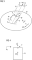
- the substrate semiconductor sample 20 is located in the xy plane and the ion beam, the FIB axis forms an angle ⁇ with the surface of the wafer 20 which should be milled at position A as shown and under normal circumstances a scan line 52 is used which is extending parallel to the top surface of the sample 20.
- the scan line is parallel to the x-axis and the milling occurs in direction of the y-axis.
- the mill angle ⁇ ' corresponds to the incidence angle ⁇ which indicates the angle between the milled surface 25 and the top surface of the sample here indicated by reference numeral 26.
- the sample orientation mark, SOM 28 is shown representing the rotation around the z axis.
- Fig. 4 shows the top-down view with the milled surface 25 when seen in the direction of the z-axis.
- the scan line of the ion beam can now be changed by the angle ⁇ resulting in an adapted scan line 53 which has the angle ⁇ relative to the default or initial scan line parallel to the x-axis in Fig 3 .
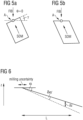
- the mill direction changes but also the milled plane changes as shown in Figures 5A and 5B.
- Fig. 5A shows the situation when the scan angle is not amended so that ⁇ is zero and the sample is rotated by the rotation angle ⁇ , as indicated.
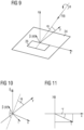
- equation 1 will be explained in connection with Figures 9-11 further below when the ion beam scan angle ⁇ is not 0, the effective angle of the milled plane also changes from ⁇ to ⁇ ' ( ⁇ ) .
- Each of the solutions a) and b) can be applied alone, however both solutions may also be applied at the same time.
- small angle rocking is to keep the variation ⁇ ' of ⁇ ' below an acceptance limit delimiting the rocking amplitude ⁇ applied around some mean sample rotation angle ⁇ as seen in Fig 1 .
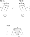
- a rocking alternating between + ⁇ and - ⁇ will mill a wedge with an angle ⁇ ' as shown by Fig. 7B.
- Fig. 7A indicates the milled surface 25 for - ⁇
- Fig. 7B shows the corresponding milled surface 25 for the sample rotation + ⁇ .
- Fig. 8 shows the overall milled width W and the rocking milled region 28 which should be selected large enough for sufficient overlap over L.
- the symmetric rocking can be combined with the small angle rotation by applying ⁇ to both - ⁇ and + ⁇ .
- the change of the milling angle ⁇ ' without changing the mechanical arrangement can be achieved by using the scan rotation by changing the scan angle ⁇ .
- the ion beam may be applied to the upper top surface when the semiconductor sample was rotated by a rotation angle + ⁇ and when the sample was rotated by a rotation angle of - ⁇ , for each of the rotation angles the scan angle ⁇ can be determined and the scan line can be adapted for each of the rotation angles as determined.
- the ion beam can be applied alternately with the adapted scan line when the rotation angle is ⁇ ⁇ .
- the milled surface extending oblique to the upper top surface generated by the ion beam in the upper top surface can have a mill angle ⁇ ' with the top surface which changes with the scan angle ⁇ .
- a maximum value of the angle ⁇ to ⁇ ' for the milled top surface not to be exceeded during milling can be determined based on the rotation angle ⁇ and the incidence angle ⁇ .
- the angle ⁇ ' may be determined using Eq. 9 discussed above.
- the second aspect when the incidence angle ⁇ and the desired mill angle ⁇ ' are known it is possible to determine the scan angle ⁇ based on the incidence angle ⁇ and the desired mill angle ⁇ ' .
Landscapes
- Chemical & Material Sciences (AREA)
- Analytical Chemistry (AREA)
- Physics & Mathematics (AREA)
- Engineering & Computer Science (AREA)
- Plasma & Fusion (AREA)
- Drying Of Semiconductors (AREA)
- Electron Sources, Ion Sources (AREA)
- Sampling And Sample Adjustment (AREA)
- Analysing Materials By The Use Of Radiation (AREA)
Applications Claiming Priority (1)
| Application Number | Priority Date | Filing Date | Title |
|---|---|---|---|
| DE102023126288 | 2023-09-27 |
Publications (2)
| Publication Number | Publication Date |
|---|---|
| EP4531073A2 true EP4531073A2 (de) | 2025-04-02 |
| EP4531073A3 EP4531073A3 (de) | 2025-09-03 |
Family
ID=92909502
Family Applications (1)
| Application Number | Title | Priority Date | Filing Date |
|---|---|---|---|
| EP24202622.7A Pending EP4531073A3 (de) | 2023-09-27 | 2024-09-25 | Strahlwinkeldrehung und probenrotation |
Country Status (3)
| Country | Link |
|---|---|
| US (1) | US20250104963A1 (de) |
| EP (1) | EP4531073A3 (de) |
| TW (1) | TW202529144A (de) |
Family Cites Families (2)
| Publication number | Priority date | Publication date | Assignee | Title |
|---|---|---|---|---|
| EP1209737B2 (de) * | 2000-11-06 | 2014-04-30 | Hitachi, Ltd. | Verfahren zur Herstellung von Proben |
| JP6753679B2 (ja) * | 2016-03-25 | 2020-09-09 | 株式会社日立ハイテクサイエンス | 制御装置、荷電粒子ビーム装置、プログラム及び加工品を生産する方法 |
-
2024
- 2024-09-25 EP EP24202622.7A patent/EP4531073A3/de active Pending
- 2024-09-26 US US18/897,888 patent/US20250104963A1/en active Pending
- 2024-09-26 TW TW113136772A patent/TW202529144A/zh unknown
Also Published As
| Publication number | Publication date |
|---|---|
| TW202529144A (zh) | 2025-07-16 |
| EP4531073A3 (de) | 2025-09-03 |
| US20250104963A1 (en) | 2025-03-27 |
Similar Documents
| Publication | Publication Date | Title |
|---|---|---|
| US12557588B2 (en) | Methods of cross-section imaging of an inspection volume in a wafer | |
| US20220138973A1 (en) | Cross section imaging with improved 3d volume image reconstruction accuracy | |
| US9733164B2 (en) | Lamella creation method and device using fixed-angle beam and rotating sample stage | |
| JP6644127B2 (ja) | 荷電粒子ビーム試料作製におけるカーテニングを低減させる方法およびシステム | |
| JPWO2020100179A1 (ja) | 画像形成方法及び画像形成システム | |
| TW202407742A (zh) | 具有增加處理量與準確度的半導體晶圓3d體積檢查 | |
| EP4531073A2 (de) | Strahlwinkeldrehung und probenrotation | |
| US20250299915A1 (en) | Image generation with improved scanning lines for smart charge distribution | |
| TWI899942B (zh) | 使用聚焦線測量高度 | |
| US12451323B2 (en) | Flow for high resolution stereoscopic measurements | |
| US12548734B2 (en) | In-line depth measurements by AFM | |
| US20250054726A1 (en) | Method to more precisely calibrate the mechanical tilt and rotation angles of an sem column | |
| WO2025261786A1 (en) | 3d inspection of buried regions of interest with reduced milling artefacts | |
| US20260094263A1 (en) | Structure determination | |
| TWI911779B (zh) | 利用雙束裝置擷取三維(3d)體積影像的方法及雙束系統 | |
| Lee et al. | Automated Diagonal Slice and View Solution for 3D Device Structure Analysis | |
| JPH06308039A (ja) | 異物分析装置 | |
| WO2025223848A1 (en) | Inspection apparatus for 3D tomography with improved stand-still performance | |
| KR100552560B1 (ko) | 주사 전자현미경 분석용 시편 제조방법 | |
| TW202609847A (zh) | 對具有降低的銑削製品的埋藏感興趣區域進行3d檢查 | |
| WO2026017513A1 (en) | Method of operating a dual beam device and corresponding apparatus | |
| WO2024088923A1 (en) | Improved method and apparatus for segmentation of semiconductor inspection images | |
| WO2024175376A1 (en) | 3d volume inspection method and method of configuring of a 3d volume inspection method | |
| TW202609842A (zh) | 晶圓中檢測體積的橫斷面成像之方法、電腦程式產品以及雙波束裝置 |
Legal Events
| Date | Code | Title | Description |
|---|---|---|---|
| PUAI | Public reference made under article 153(3) epc to a published international application that has entered the european phase |
Free format text: ORIGINAL CODE: 0009012 |
|
| STAA | Information on the status of an ep patent application or granted ep patent |
Free format text: STATUS: THE APPLICATION HAS BEEN PUBLISHED |
|
| AK | Designated contracting states |
Kind code of ref document: A2 Designated state(s): AL AT BE BG CH CY CZ DE DK EE ES FI FR GB GR HR HU IE IS IT LI LT LU LV MC ME MK MT NL NO PL PT RO RS SE SI SK SM TR |
|
| PUAL | Search report despatched |
Free format text: ORIGINAL CODE: 0009013 |
|
| AK | Designated contracting states |
Kind code of ref document: A3 Designated state(s): AL AT BE BG CH CY CZ DE DK EE ES FI FR GB GR HR HU IE IS IT LI LT LU LV MC ME MK MT NL NO PL PT RO RS SE SI SK SM TR |
|
| RIC1 | Information provided on ipc code assigned before grant |
Ipc: H01J 37/304 20060101AFI20250729BHEP Ipc: H01J 37/302 20060101ALI20250729BHEP Ipc: H01J 37/305 20060101ALI20250729BHEP Ipc: H01J 37/30 20060101ALI20250729BHEP |