EP4530249A1 - Mikroelektromechanisches bauelement mit spaltsteuerungsstruktur und verfahren zu seiner herstellung - Google Patents
Mikroelektromechanisches bauelement mit spaltsteuerungsstruktur und verfahren zu seiner herstellung Download PDFInfo
- Publication number
- EP4530249A1 EP4530249A1 EP23200481.2A EP23200481A EP4530249A1 EP 4530249 A1 EP4530249 A1 EP 4530249A1 EP 23200481 A EP23200481 A EP 23200481A EP 4530249 A1 EP4530249 A1 EP 4530249A1
- Authority
- EP
- European Patent Office
- Prior art keywords
- wafer
- metal layer
- cap wafer
- gap
- cap
- Prior art date
- Legal status (The legal status is an assumption and is not a legal conclusion. Google has not performed a legal analysis and makes no representation as to the accuracy of the status listed.)
- Granted
Links
Images


Classifications
-
- B—PERFORMING OPERATIONS; TRANSPORTING
- B81—MICROSTRUCTURAL TECHNOLOGY
- B81C—PROCESSES OR APPARATUS SPECIALLY ADAPTED FOR THE MANUFACTURE OR TREATMENT OF MICROSTRUCTURAL DEVICES OR SYSTEMS
- B81C1/00—Manufacture or treatment of devices or systems in or on a substrate
- B81C1/00015—Manufacture or treatment of devices or systems in or on a substrate for manufacturing microsystems
- B81C1/00261—Processes for packaging MEMS devices
- B81C1/00269—Bonding of solid lids or wafers to the substrate
-
- B—PERFORMING OPERATIONS; TRANSPORTING
- B81—MICROSTRUCTURAL TECHNOLOGY
- B81B—MICROSTRUCTURAL DEVICES OR SYSTEMS, e.g. MICROMECHANICAL DEVICES
- B81B7/00—Microstructural systems; Auxiliary parts of microstructural devices or systems
- B81B7/0032—Packages or encapsulation
- B81B7/0077—Other packages not provided for in groups B81B7/0035 - B81B7/0074
-
- B—PERFORMING OPERATIONS; TRANSPORTING
- B81—MICROSTRUCTURAL TECHNOLOGY
- B81B—MICROSTRUCTURAL DEVICES OR SYSTEMS, e.g. MICROMECHANICAL DEVICES
- B81B2203/00—Basic microelectromechanical structures
- B81B2203/03—Static structures
- B81B2203/0307—Anchors
-
- B—PERFORMING OPERATIONS; TRANSPORTING
- B81—MICROSTRUCTURAL TECHNOLOGY
- B81B—MICROSTRUCTURAL DEVICES OR SYSTEMS, e.g. MICROMECHANICAL DEVICES
- B81B2203/00—Basic microelectromechanical structures
- B81B2203/03—Static structures
- B81B2203/0315—Cavities
-
- B—PERFORMING OPERATIONS; TRANSPORTING
- B81—MICROSTRUCTURAL TECHNOLOGY
- B81B—MICROSTRUCTURAL DEVICES OR SYSTEMS, e.g. MICROMECHANICAL DEVICES
- B81B2207/00—Microstructural systems or auxiliary parts thereof
- B81B2207/07—Interconnects
-
- B—PERFORMING OPERATIONS; TRANSPORTING
- B81—MICROSTRUCTURAL TECHNOLOGY
- B81B—MICROSTRUCTURAL DEVICES OR SYSTEMS, e.g. MICROMECHANICAL DEVICES
- B81B2207/00—Microstructural systems or auxiliary parts thereof
- B81B2207/09—Packages
- B81B2207/091—Arrangements for connecting external electrical signals to mechanical structures inside the package
- B81B2207/094—Feed-through, via
- B81B2207/095—Feed-through, via through the lid
-
- B—PERFORMING OPERATIONS; TRANSPORTING
- B81—MICROSTRUCTURAL TECHNOLOGY
- B81C—PROCESSES OR APPARATUS SPECIALLY ADAPTED FOR THE MANUFACTURE OR TREATMENT OF MICROSTRUCTURAL DEVICES OR SYSTEMS
- B81C2201/00—Manufacture or treatment of microstructural devices or systems
- B81C2201/01—Manufacture or treatment of microstructural devices or systems in or on a substrate
- B81C2201/0101—Shaping material; Structuring the bulk substrate or layers on the substrate; Film patterning
- B81C2201/0128—Processes for removing material
- B81C2201/013—Etching
-
- B—PERFORMING OPERATIONS; TRANSPORTING
- B81—MICROSTRUCTURAL TECHNOLOGY
- B81C—PROCESSES OR APPARATUS SPECIALLY ADAPTED FOR THE MANUFACTURE OR TREATMENT OF MICROSTRUCTURAL DEVICES OR SYSTEMS
- B81C2201/00—Manufacture or treatment of microstructural devices or systems
- B81C2201/01—Manufacture or treatment of microstructural devices or systems in or on a substrate
- B81C2201/0174—Manufacture or treatment of microstructural devices or systems in or on a substrate for making multi-layered devices, film deposition or growing
-
- B—PERFORMING OPERATIONS; TRANSPORTING
- B81—MICROSTRUCTURAL TECHNOLOGY
- B81C—PROCESSES OR APPARATUS SPECIALLY ADAPTED FOR THE MANUFACTURE OR TREATMENT OF MICROSTRUCTURAL DEVICES OR SYSTEMS
- B81C2203/00—Forming microstructural systems
- B81C2203/01—Packaging MEMS
- B81C2203/0109—Bonding an individual cap on the substrate
-
- B—PERFORMING OPERATIONS; TRANSPORTING
- B81—MICROSTRUCTURAL TECHNOLOGY
- B81C—PROCESSES OR APPARATUS SPECIALLY ADAPTED FOR THE MANUFACTURE OR TREATMENT OF MICROSTRUCTURAL DEVICES OR SYSTEMS
- B81C2203/00—Forming microstructural systems
- B81C2203/01—Packaging MEMS
- B81C2203/0118—Bonding a wafer on the substrate, i.e. where the cap consists of another wafer
-
- B—PERFORMING OPERATIONS; TRANSPORTING
- B81—MICROSTRUCTURAL TECHNOLOGY
- B81C—PROCESSES OR APPARATUS SPECIALLY ADAPTED FOR THE MANUFACTURE OR TREATMENT OF MICROSTRUCTURAL DEVICES OR SYSTEMS
- B81C2203/00—Forming microstructural systems
- B81C2203/03—Bonding two components
- B81C2203/033—Thermal bonding
- B81C2203/035—Soldering
Definitions
- This disclosure relates to electronic devices and more particularly to Microelectromechanical components.
- the present disclosure further concerns eutectic bonding of microelectromechanical components with a gap-control structure.
- MEMS Microelectromechanical systems
- MEMS devices also called MEMS elements, can have either simple or complex structures with various moving parts. They include devices such as gyroscopes, acceleration sensors, magnetometers, and pressure sensors. MEMS devices may be fabricated from a silicon wafer by microfabrication techniques.
- Electronic chips also called dies, are prepared by manufacturing various electronic structures on a substrate and cutting the substrate into small, chip-size pieces. These chips may be MEMS devices. Several MEMS elements may be built on the same die. This allows significant cost and area reduction. Once the MEMS elements are built, they may need to be sealed in a particular environment depending on their function.
- Eutectic bonding also known as eutectic soldering, is a well-established semiconductor bonding technology that involves bonding wafers together by high pressure using a seal formed of two or more metal films which transform into a eutectic alloy at a specific temperature (eutectic temperature). Due to their easy preparation techniques and good wettability, eutectic alloys form excellent seals in electronic devices. Eutectic bonding is widely used in MEMS technology for the hermetic sealing of MEMS components. During the bonding process, at the eutectic temperature, the eutectic alloy is in a liquid phase. Because bonding process involves pressing wafers together at high pressure, in some circumstances, it may be challenging to accurately control the gap height between the bonded wafers, and thus the MEMS element cavity height, due to the softness of the liquid eutectic alloy.
- An object of the present disclosure is to provide a solution to the problem described above.
- the disclosed solution allows MEMS vertical gap height control in eutectically bonded microelectromechanical components. Examples provided in this disclosure describe ways to implement the solution. The improvement is achieved by features of the microelectromechanical component and a manufacturing method.
- the disclosure is based on the idea of including a structure comprising a standoff and an adjacent eutectic anchor inside the MEMS element.
- the standoff provides an accurate control of the MEMS gap height during the eutectic bonging of the component whereas the anchor improves the mechanical anchoring of the standoff.
- the structure provides new improvements of gap control and robustness of the eutectic bond in the microelectromechanical component.
- the disclosure describes a microelectromechanical component comprising a cap wafer and a structure wafer.
- the cap wafer has a top surface and a bottom surface.
- the top surface of the cap wafer defines a horizontal xy-plane and a vertical z-direction which is perpendicular to the xy-plane.
- the cap wafer comprises a cap wafer sealing region and a cap wafer gap-control region, and the cap wafer sealing region surrounds the cap wafer gap-control region.
- the structure wafer has a top surface and a bottom surface, and the top surface of the structure wafer is parallel to the xy-plane.
- the structure wafer comprises a structure wafer sealing region and a structure wafer gap-control region, and the structure wafer sealing region surrounds the structure wafer gap-control region.
- the cap wafer and the structure wafer are bonded to each other by a eutectic seal which connects the cap wafer sealing region to the structure wafer sealing region so that the cap wafer gap-control region is aligned with the structure wafer gap-control region along the z-axis.
- the microelectromechanical component further comprises a metal layer. The metal layer is located at the bottom surface of the cap wafer in the cap wafer gap-control region.
- the structure wafer further comprises a standoff in the structure wafer gap-control region.
- the standoff protrudes outward from the top surface of the structure wafer and extends along the z-direction so that it meets the metal layer.
- the microelectromechanical component further comprises at least one eutectic anchor attached to the top surface of the structure wafer in the structure wafer gap-control region next to the standoff.
- the eutectic anchor extends along the z-direction from the top surface of the structure wafer to the bottom surface of the cap wafer.
- any direction or plane which is parallel to the xy-plane defined by the cap wafer can be called horizontal.
- the direction which is perpendicular to the xy-plane can be called vertical direction.
- Expressions such as “top”, “bottom”, “above”, “below”, “up” and “down” refer in this disclosure to differences in the vertical z-coordinate. These expressions do not imply anything about how the device should be oriented with respect to the earth's gravitational field when the component is in use or when it is being manufactured.
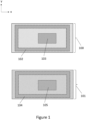
- FIG. 1 illustrates an example of a bottom view of a cap wafer and a top view of a structure wafer.
- the cap wafer 100 comprises a cap wafer gap-control region 103 and a cap wafer sealing region 102.
- the cap wafer sealing region 102 is adjacent to the edges of the cap wafer.
- the cap wafer sealing region 102 surrounds the cap wafer gap-control region 103.
- the structure wafer 101 comprises a structure wafer gap-control region 105 and a structure wafer sealing region 104.
- the structure wafer sealing region 104 is adjacent to the edges of the structure wafer.
- the structure wafer sealing region 104 surrounds the structure wafer gap-control region 105.
- the cap wafer 100 and the structure wafer 101 may be bonded to each other so that a eutectic seal connects the cap wafer sealing region 102 to the structure wafer sealing region 104 and the cap wafer gap-control region 103 is aligned with the structure wafer gap-control region 105 along the z-axis.
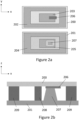
- Figure 2a illustrates a simplified example of a bottom view of a cap wafer and a top view of a structure wafer in a microelectromechanical component.
- the cap wafer 200 comprises a cap wafer sealing region 202 which is adjacent to the edges of the cap wafer 200.
- the cap wafer 200 further comprises a cap wafer gap-control region 203.
- the cap wafer sealing region 202 surrounds the cap wafer gap-control region 203.
- a metal layer 206 is attached to the bottom surface of the cap wafer 200 in the cap wafer gap-control region 203.
- the metal layer 206 extends outside the cap wafer gap-control region.
- the metal layer may be located within the cap-wafer gap control region 203.
- the structure wafer 201 comprises a structure wafer sealing region 204.
- the structure wafer sealing region 204 is adjacent to the edges of the structure wafer 201.
- the structure wafer 201 further comprises a structure wafer gap-control region 205.
- the structure wafer sealing region 204 surrounds the structure wafer gap-control region 205.
- the structure wafer 201 further comprises a standoff 207 located in the structure wafer gap-control region 205.
- the standoff 207 protrudes in the z-direction outward from the top surface of the structure wafer 201.
- the microelectromechanical component may comprise a plurality of standoffs.
- the standoff shape may for example be a truncated pyramid shape, or a pillar-like shape.
- the pillar like-shape may be, but is not limited to, a cylinder, a hexagonal prism, or a cuboid. These options may apply to any embodiment in this disclosure.
- the standoff 207 has a truncated pyramid shape.
- Figure 2b illustrates a sectional view of the microelectromechanical component comprising the cap wafer and structure wafer shown in figure 2a .
- the cap wafer 200 and the structure wafer 201 are bonded to each other by a eutectic seal 209 which connects the cap wafer sealing region to the structure wafer sealing region so that the cap wafer gap-control region is aligned with the structure wafer gap-control region along the z-axis.
- the standoff 207 which has a truncated pyramid shape, protrudes outward from the top surface of the structure wafer 201 and extends along the z-direction so that it meets the metal layer 206.
- the microelectromechanical component further comprises a eutectic anchor 208 which is attached to the top surface of the structure wafer 201 in the structure wafer gap-control region next to the standoff.
- the eutectic anchor 208 extends along the z-direction from the top surface of the structure wafer 201 to the bottom surface of the cap wafer 200.
- the distance, in any direction parallel to the xy-plane, between the eutectic anchor and the standoff may be less than the distance between the eutectic seal and the standoff.
- the distance, in any direction parallel to the xy-plane, between the eutectic anchor and the standoff may be in the range [5-100] ⁇ m, or [10-50] ⁇ m, or [20-80] ⁇ m, or [50-60] ⁇ m.
- the standoff 207 and the eutectic anchor 208 form a gap-control structure.
- the metal layer 206 may be made of a variety of metals that include but are not limited to Al, Cu, Ag, Au, Pt, Pd, Mo or metal alloys.
- the metal layer may be formed by a variety of deposition methods such as sputtering, chemical vapor deposition, molecular beam epitaxy, electron beam physical vapor evaporation, or laser metal deposition.
- the thickness of the metal layer 206 may be in the range [0.1-1.0] ⁇ m, or [0.1-0.5] ⁇ m, or [0.3-0.7] ⁇ m.
- the eutectic anchor may be made of a eutectic alloy formed by two or more metals which include, but are not limited to, Au-Sn, Au-In or Cu-Sn.
- the eutectic anchor may be made of an alloy comprising a metalloid.
- the eutectic anchor may be made of Ge, Al and Ti, or it may be made of Ge and Al.
- the eutectic anchor and eutectic seal may be made of the same eutectic alloy.
- the eutectic anchor and the eutectic seal may be made of different eutectic alloys.
- the structure wafer may be a semiconductor device layer which has been attached to a support layer (not illustrated).
- the device layer may be a layer of silicon.
- the device layer and the support layer may for example be parts of a silicon-on-insulator (SOI) substrate where MEMS elements can be formed by patterning the top silicon layer (the device layer).
- SOI silicon-on-insulator
- the cap wafer may be an insulating wafer such as a glass layer, or a wafer comprising semiconducting parts and insulating parts, or a wafer comprising metal parts and insulating parts.
- Figure 2c illustrates another simplified example of a bottom view of a cap wafer and a top view of a structure wafer in a microelectromechanical component.
- the standoff 217 has a pillar-like shape.
- Reference numbers 210, 211, 212, 213, 214, 215 and 216 in figure 2c correspond to reference numbers 200, 201, 202, 203, 204, 205 and 206, respectively, in figure 2a .
- Figure 2d illustrates a sectional view of the microelectromechanical component comprising the cap wafer and structure wafer shown in figure 2c .
- the cap wafer 210 and the structure wafer 211 are bonded to each other by a eutectic seal 219 which connects the cap wafer sealing region to the structure wafer sealing region so that the cap wafer gap-control region is aligned with the structure wafer gap-control region along the z-axis.
- the standoff 217 has a cylinder shape.
- the microelectromechanical component further comprises a eutectic anchor 218 which is attached to the top surface of the structure wafer 211 in the structure wafer gap-control region next to the standoff.
- the eutectic anchor 218 extends along the z-direction from the top surface of the structure wafer 211 to the bottom surface of the cap wafer 210.
- the standoff 217 and the eutectic anchor 218 form a gap-control structure.
- Reference number 216 in figure 2d corresponds to reference number 206 in figure 2a .
- the microelectromechanical component may comprise one or more eutectic anchors.
- a plurality of eutectic anchors may be substantially evenly distributed around the standoff.
- a single eutectic anchor may surround the standoff.
- the ratio of the surface area of the eutectic anchor to the surface area of the standoff in the xy-plane may be in the range [1:10-10:1] or [1:3-3:1].
- Figures 3a-3c illustrate different possible shapes and positions of eutectic anchors in a microelectromechanical component.
- Figure 3a illustrates an example of a simplified top view of the structure wafer 301 in a microelectromechanical component.
- the microelectromechanical component comprises a single eutectic anchor 308 which is adjacent to the standoff 307.
- Reference numbers 304 and 305 in figure 3a correspond to reference numbers 204 and 205, respectively, in figure 2a .
- Reference number 309 in figure 3a corresponds to reference number 209 in figure 2b .
- Figure 3b illustrates another example of a simplified top view of the structure wafer in a microelectromechanical component.
- the microelectromechanical component comprises two eutectic anchors 318 which are adjacent to the standoff 317.
- the eutectic anchors 318 are located opposite to each other on different sides of the standoff 317.
- Reference numbers 311, 314 and 315 in figure 3b correspond to reference numbers 201, 204 and 205, respectively, in figure 2a .
- Reference number 319 in figure 3b corresponds to reference number 209 in figure 2b .
- Figure 3c illustrates another example of a simplified top view of the structure wafer in a microelectromechanical component.
- the microelectromechanical component comprises one eutectic anchor 328 surrounding the standoff 327.
- Reference numbers 321, 324 and 325 in figure 3c correspond to reference numbers 201, 204 and 205, respectively, in figure 2a .
- Reference number 329 in figure 3c corresponds to reference number 209 in figure 2b .
- the cap wafer may comprise at least one electrically conductive via wherein the electrically conductive via extends along the z-axis through the cap wafer so that it meets the metal layer.
- the electrically conductive via may extend through at least a portion of the cap wafer thickness. Alternatively, the electrically conductive via may extend through the whole cap wafer thickness.
- FIG 4a illustrates a simplified example of a sectional view of a microelectromechanical component comprising a gap-control structure.
- the microelectromechanical component comprises a cap wafer 400 and a structure wafer 401 which are bonded together via a eutectic seal 409.
- the cap wafer 400 comprises an electrically conductive via 4010 which extends through the whole cap wafer thickness.
- the microelectromechanical component further comprises a metal layer 406, which is located at the bottom side of cap wafer in the cap wafer gap-control region.
- the metal layer 406 extends along the bottom surface of the cap wafer so that it meets the bottom side of the electrically conductive via 4010.
- the cap wafer may be made of an insulating material such as glass.
- the electrically conductive via may be a semiconducting via.
- the electrically conductive via may be a metal via.
- the metal layer 406 may be connected to an external electrical connection through the electrically conductive via 4010.
- Reference numbers 407 and 408 in figure 4a correspond to reference numbers 207 and 208, respectively, in figure 2b .
- the cap wafer may comprise a metal part and an insulating part, wherein the metal part is located on top of the insulating part so that the bottom surface of the insulating part forms the bottom surface of the cap wafer.
- the cap wafer may further comprise at least one electrically conductive via.
- the electrically conductive via may extend along the z-axis from the bottom side of the metal part to the bottom side of the insulating part so that the insulating part surrounds the sides of the electrically conductive via.
- the metal layer may extend along the bottom surface of the insulating part so that it meets the bottom side of the electrically conductive via
- Figure 4b illustrates another example of a sectional view of a microelectromechanical component with a gap-control structure.
- the microelectromechanical component comprises a cap wafer 410 and a structure wafer 411 which are bonded together via a eutectic seal 419.
- the cap wafer comprises a semiconducting part and an insulating part.
- the semiconducting part 4111 is located on top of the insulating part 4112 so that the bottom surface of the insulating part forms the bottom surface of the cap wafer.
- the cap wafer 410 further comprises an electrically conductive via 4110 which extend along the z-axis from the bottom side of the semiconducting part 4111 to the bottom side of the insulating part 4112 so that the insulating part surrounds the sides of the electrically conductive via 4110.
- the microelectromechanical component further comprises a metal layer 416, which is located at the bottom side of cap wafer in the cap wafer gap-control region. The metal layer 416 extends along the bottom surface of the insulating part so that it meets the bottom side of the electrically conductive via 4110.
- the electrically conductive via may be a semiconducting via. Alternatively, the electrically conductive via may be a metal via.
- the metal layer 416 may be connected to an external electrical connection through the electrically conductive via 4110.
- the structure wafer 411 comprises a standoff 417 which is located in the structure wafer gap-control region.
- the standoff 417 protrudes in the z-direction outward from the top surface of the structure wafer 411 so that it meets the metal layer 416.
- the standoff 417 and the metal layer 416 may serve as a good ohmic press-on contact inside the element.
- the standoff 417 and the adjacent eutectic anchor 418 serve as an accurate gap-height control structure as the eutectic anchor 418 contributes to securing a stable contact between the standoff 417 and the metal layer 416.
- the eutectic anchor adds mechanical strength to the structure making it robust to lifetime testing.
- FIGS 5a-5f provide a simplified illustration of an example method for manufacturing a microelectromechanical component with a gap-control structure.
- the microelectromechanical component comprises a cap wafer and a structure wafer.
- the cap wafer has a top surface and a bottom surface.
- the top surface of the cap wafer defines a horizontal xy-plane and a vertical z-direction which is perpendicular to the xy-plane.
- the cap wafer comprises a cap wafer sealing region and a cap wafer gap-control region, and the cap wafer sealing region surrounds the cap wafer gap-control region.
- the structure wafer has a top surface and a bottom surface.
- the top surface of the structure wafer is parallel to the xy-plane.
- the structure wafer comprises a structure wafer sealing region and a structure wafer gap-control region, and the structure wafer sealing region surrounds the structure wafer gap-control region.
- the method comprises: (1) forming a first metal layer on the bottom surface of the cap wafer in the cap wafer gap-control region, (2) forming a second metal layer on the bottom surface of the cap wafer next to the first metal layer in the cap wafer gap-control region, (3) forming a standoff in the structure wafer gap-control region so that the standoff protrudes outward from the top surface of the structure wafer and extends in the z-direction, (4) forming a third metal layer on the top surface of the structure wafer next to the standoff in the structure wafer gap-control region, (5) placing the cap wafer on top of the structure wafer so that the first metal layer is aligned with the standoff along the z-axis and the second metal layer is aligned with the third metal layer along the z-axis, (6) bonding the cap wafer sealing region and the structure wafer sealing region together so that the top surface of the standoff is connected to the first metal layer, and the second metal layer and the third metal layer form a eutectic anchor
- the structure wafer may be a semiconductor device layer which has been attached to a support layer.
- the device layer may be a layer of silicon.
- the device layer and the support layer may for example be parts of a silicon-on-insulator (SOI) substrate where MEMS elements can be formed by patterning the top silicon layer (the device layer).
- SOI silicon-on-insulator
- the method for manufacturing a microelectromechanical component with a gap-control structure may comprise the step of forming a dielectric/insulating layer on the top surface of the structure wafer before forming the third metal layer.
- the dielectric/insulating layer has the advantage of preventing possible chemical reactions between the eutectic anchor and the structure wafer.
- the dielectric/insulating layer may be an oxide or a nitride such as SiO 2 , ZrO 2 , HfO 2 , Ta 2 O 3 , or SiNx. This option may apply to any embodiment in this disclosure.
- the cap wafer may be an insulating wafer such as a glass layer, or a wafer comprising semiconducting parts and insulating parts, or a wafer comprising metal parts and insulating parts.
- the cap wafer may for example comprise a semiconducting part and an insulating part, wherein the semiconducting part is located on top of the insulating part so that the bottom surface of the insulating part forms the bottom surface of the cap wafer.
- the cap wafer may further comprise at least one electrically conductive via.
- the electrically conductive via may extend along the z-axis from the bottom side of the semiconducting part to the bottom side of the insulating part so that the insulating part surrounds the sides of the electrically conductive via.
- the first metal layer may extend along the bottom surface of the insulating part so that it meets the bottom side of the electrically conductive via.
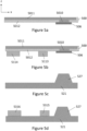
- Figure 5a illustrates one of the first steps of the example method for manufacturing a microelectromechanical component with a gap-control structure.
- the cap wafer 500 comprises a semiconducting part 5011 and an insulating part 5012.
- the semiconducting part 5011 is located on top of the insulating part 5012 so that the bottom surface of the insulating part forms the bottom surface of the cap wafer 500.
- the cap wafer 500 further comprises an electrically conductive via 5010 which extend along the z-axis from the bottom side of the semiconducting part 5011 to the bottom side of the insulating part 5012 so that the insulating part surrounds the sides of the electrically conductive via 5010.
- This step comprises forming a first metal layer 506 on the bottom surface of the cap wafer 500 in the cap wafer gap-control region so that the first metal layer 506 meets the bottom of the electrically conductive via 5010.
- the first metal layer may be made of a variety of metals that include but are not limited to Al, Cu, Ag, Au, Pt, Pd, Mo or metal alloys.
- the first metal layer may be formed by a variety of deposition methods such as sputtering, chemical vapor deposition, molecular beam epitaxy, electron beam physical vapor evaporation, or laser metal deposition.
- the thickness of the first metal layer 506 may be in the range [0.1-1.0] ⁇ m, or [0.1-0.5] ⁇ m, or [0.3-0.7] ⁇ m.
- the electrically conductive via may be a semiconducting via. Alternatively, the electrically conductive via may be a metal via.
- Figure 5b illustrates another step in the method for manufacturing a microelectromechanical component with a gap-control structure.
- a second metal layer 5113 is formed on the bottom surface of the cap wafer in the cap wafer gap-control region next to the first metal layer 506.
- a first additional metal layer 5114 may simultaneously be formed in the cap wafer sealing region.
- the second metal layer 5113 and the first additional metal layer 5114 may be made of the same metal.
- the second metal layer 5113 and the first additional metal layer 5114 may be made of different metals.
- Figure 5c illustrates another step in the method for manufacturing a microelectromechanical component with a gap-control structure.
- a standoff 527 is formed in the structure wafer gap-control region so that the standoff protrudes outward from the top surface of the structure wafer 521 and extends in the z-direction.
- the standoff 527 may be formed by semiconductor microfabrication techniques such as LOCOS process, wet etching process or dry etching process.
- Figure 5d illustrates a further step in the method for manufacturing a microelectromechanical component with a gap-control structure.
- a third metal layer 5315 is formed on the top surface of the structure wafer 521 in the structure wafer gap-control region next to the standoff 527.
- a second additional metal layer 5316 may simultaneously be formed in the structure wafer sealing region.
- the third metal layer 5315 and the second additional metal layer 5316 may be made of the same metal.
- the third metal layer 5315 and the second additional metal layer 5316 may be made of different metals.
- the second metal layer 5113 and the third metal layer 5315 may be made of any metals that form a eutectic alloy at a corresponding eutectic temperature.
- the first additional metal layer 5114 and the second additional metal layer 5316 may be made of any metals that form a eutectic alloy at a corresponding eutectic temperature.
- Such metals may include, but are not limited to, Au- Sn, Au-In or Cu-Sn. These options may apply to any embodiment in this disclosure.
- Figure 5f illustrates the final step of the example method for manufacturing a microelectromechanical component with a gap-control structure.
- the cap wafer 500 and structure wafer 521 are pressed together at a specific eutectic temperature. Consequently, the cap wafer sealing region and the structure wafer sealing region are bonded together through the eutectic seal 549 formed by the chemical reaction between the first additional metal layer 5114 and the second additional metal layer 5316.
- the standoff 527 comes into contact with the first metal layer 506 and a eutectic anchor 548 is formed by the chemical reaction between the second metal layer 5113 and the third metal layer 5315.
- the eutectic temperature may be in the range [300-500]°C, [400-450]°C, or [420-450]°C.
- the standoff 527 and the first metal layer 506 may serve as a good ohmic press-on contact inside the MEMS element after the eutectic bonding.
- the standoff 527 and the adjacent eutectic anchor 548 form an accurate gap-height control structure as the eutectic anchor 548 contributes to securing a stable contact between the standoff 527 and the first metal layer 506.
- the method for manufacturing a microelectromechanical component with a gap-control structure may further comprise the steps of forming a metalloid layer on top of the third metal layer before placing the cap wafer on top of the structure wafer, then bonding the cap wafer and the structure wafer together so that the second metal layer, the third metal layer and the metalloid layer form a eutectic anchor.
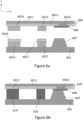
- Figure 6a illustrates an example of a microelectromechanical component before the cap wafer and the structure wafer are bonded together.
- a metalloid layer 6017 is formed on top of the third metal layer 6015 before the eutectic bonding step.
- an additional metalloid layer 6018 may be formed on top of the second additional metal layer 6016 before the eutectic bonding step.
- the second metal layer 6013 may be an Al layer
- the third metal layer 6015 may be a Ti layer
- the metalloid layer 6017 may be a Ge layer.
- Reference numbers, 600, 601, 606, 607, 6010, 6011, 6012 and 6014 in figure 6a correspond to reference numbers 500, 521, 506, 527, 5010, 5011, 5012 and 5114, respectively, in figure 5e .
- Figure 6b illustrates the electromechanical component shown in figure 6a after the eutectic bonding of the cap wafer 600 and the structure wafer 601 together at eutectic temperature.
- the cap wafer sealing region and the structure wafer sealing region are bonded together through the eutectic seal 619 formed by the chemical reaction between of the first additional metal layer 6014, the second additional metal layer 6016, and the additional metalloid layer 6018.
- the standoff 607 meets the first metal layer 606 and a eutectic anchor 618 is formed by the chemical reaction between the second metal layer 6013, the third metal layer 6015, and the metalloid layer 6017.
- Reference numbers 6010, 6011 and 6012 in figure 6b correspond to reference numbers 5010, 5011 and 5012, respectively, in figure 5a .
- the method for manufacturing a microelectromechanical component may further comprise the steps of forming a metalloid layer at the bottom of the second metal layer before placing the cap wafer on top of the structure wafer, then bonding the cap wafer and the structure wafer together so that the second metal layer, the third metal layer and the metalloid layer form a eutectic anchor.
- Figure 7a illustrates another example of a microelectromechanical component before the cap wafer and the structure wafer are bonded together.
- a metalloid layer 7017 is formed at the bottom of the second metal layer 7013 before the eutectic bonding step.
- an additional metalloid layer 7018 may be formed at the bottom of the first additional metal layer 7014 before the eutectic bonding step.
- Reference numbers 700, 701, 706, 707, 7010, 7011, 7012, 7015 and 7016 in figure 7a correspond to reference numbers 500, 521, 506, 527, 5010, 5011, 5012, 5315 and 5316, respectively, in figure 5e .
- Figure 7b illustrates the electromechanical component shown in figure 7a after the eutectic bonding of the cap wafer 700 and the structure wafer 701 together at eutectic temperature.
- the cap wafer sealing region and the structure wafer sealing region are bonded together through the eutectic seal 719 formed by the chemical reaction between of the first additional metal layer 7014, the second additional metal layer 7016, and the additional metalloid layer 7018.
- the standoff 707 meets the first metal layer 706 and a eutectic anchor 718 is formed by the chemical reaction between the second metal layer 7013, the third metal layer 7015, and the metalloid layer 7017.
- the second metal layer may be a Ti layer
- the third metal layer may be an Al layer
- the metalloid layer may be a Ge layer.
- Reference numbers 7010, 7011 and 7012 in figure 7b correspond to reference numbers 5010, 5011 and 5012, respectively, in figure 5a .
- the eutectic anchor may be made of a eutectic alloy comprising only one metal layer and one metalloid layer such as an Al-Ge eutectic alloy.
- the metalloid layer may be formed either on the top surface of the structure wafer or on the bottom surface of the cap wafer.
- the eutectic seal may be made of a eutectic alloy comprising only one metal layer and one metalloid layer.
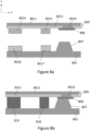
- Figure 8a illustrates a simplified example of a sectional view of a microelectromechanical component comprising a gap-control structure before and after bonding.
- the metalloid layer 8017 is formed on the top surface of the structure wafer 801 next to the standoff 807 in the structure wafer gap-control region.
- An additional metalloid layer 8018 may simultaneously be formed on the top surface of the structure wafer in the structure wafer sealing region.
- Reference numbers 800, 806, 8010, 8011, 8012, 8013 and 8014 in figure 8a correspond to reference 500, 506, 5010, 5011, 5012, 5113 and 5114, respectively, in figure 5b .
- Figure 8b illustrates the electromechanical component shown in figure 8a after the eutectic bonding of the cap wafer 800 and the structure wafer 801 together at eutectic temperature.
- the cap wafer sealing region and the structure wafer sealing region are bonded together through the eutectic seal 819 formed by the chemical reaction between of the first additional metal layer 8014 and the additional metalloid layer 8018.
- the standoff 807 comes into contact with the first metal layer 806 and a eutectic anchor 818 is formed by the chemical reaction between the second metal layer 8013 and the metalloid layer 8017.
- Reference numbers 8010, 8011 and 8012 in figure 8b correspond to reference numbers 5010, 5011 and 5012, respectively, in figure 5a .
Landscapes
- Engineering & Computer Science (AREA)
- Microelectronics & Electronic Packaging (AREA)
- Manufacturing & Machinery (AREA)
- Computer Hardware Design (AREA)
- Micromachines (AREA)
- Measuring Fluid Pressure (AREA)
- Pressure Sensors (AREA)
- Wire Bonding (AREA)
Priority Applications (4)
| Application Number | Priority Date | Filing Date | Title |
|---|---|---|---|
| EP23200481.2A EP4530249B1 (de) | 2023-09-28 | 2023-09-28 | Mikroelektromechanisches bauelement mit spaltsteuerungsstruktur und verfahren zu seiner herstellung |
| TW113133254A TWI915944B (zh) | 2023-09-28 | 2024-09-03 | 微機電構件及其製造方法 |
| US18/894,715 US20250109015A1 (en) | 2023-09-28 | 2024-09-24 | Microelectromechanical component with gap-control structure and a method for manufacturing it |
| CN202411349296.8A CN119706730A (zh) | 2023-09-28 | 2024-09-26 | 具有间隙控制结构的微机电部件及其制造方法 |
Applications Claiming Priority (1)
| Application Number | Priority Date | Filing Date | Title |
|---|---|---|---|
| EP23200481.2A EP4530249B1 (de) | 2023-09-28 | 2023-09-28 | Mikroelektromechanisches bauelement mit spaltsteuerungsstruktur und verfahren zu seiner herstellung |
Publications (2)
| Publication Number | Publication Date |
|---|---|
| EP4530249A1 true EP4530249A1 (de) | 2025-04-02 |
| EP4530249B1 EP4530249B1 (de) | 2025-12-24 |
Family
ID=88236555
Family Applications (1)
| Application Number | Title | Priority Date | Filing Date |
|---|---|---|---|
| EP23200481.2A Active EP4530249B1 (de) | 2023-09-28 | 2023-09-28 | Mikroelektromechanisches bauelement mit spaltsteuerungsstruktur und verfahren zu seiner herstellung |
Country Status (3)
| Country | Link |
|---|---|
| US (1) | US20250109015A1 (de) |
| EP (1) | EP4530249B1 (de) |
| CN (1) | CN119706730A (de) |
Citations (3)
| Publication number | Priority date | Publication date | Assignee | Title |
|---|---|---|---|---|
| US20120112335A1 (en) * | 2009-04-30 | 2012-05-10 | Silex Microsystems Ab | Novel bonding process and bonded structures |
| US20140042596A1 (en) * | 2011-05-09 | 2014-02-13 | Rodney L. Alley | Bonded wafer structures |
| US10927004B2 (en) * | 2016-06-07 | 2021-02-23 | Robert Bosch Gmbh | Method for bonding wafers eutectically, and a wafer composite |
-
2023
- 2023-09-28 EP EP23200481.2A patent/EP4530249B1/de active Active
-
2024
- 2024-09-24 US US18/894,715 patent/US20250109015A1/en active Pending
- 2024-09-26 CN CN202411349296.8A patent/CN119706730A/zh active Pending
Patent Citations (3)
| Publication number | Priority date | Publication date | Assignee | Title |
|---|---|---|---|---|
| US20120112335A1 (en) * | 2009-04-30 | 2012-05-10 | Silex Microsystems Ab | Novel bonding process and bonded structures |
| US20140042596A1 (en) * | 2011-05-09 | 2014-02-13 | Rodney L. Alley | Bonded wafer structures |
| US10927004B2 (en) * | 2016-06-07 | 2021-02-23 | Robert Bosch Gmbh | Method for bonding wafers eutectically, and a wafer composite |
Also Published As
| Publication number | Publication date |
|---|---|
| CN119706730A (zh) | 2025-03-28 |
| TW202513453A (zh) | 2025-04-01 |
| EP4530249B1 (de) | 2025-12-24 |
| US20250109015A1 (en) | 2025-04-03 |
Similar Documents
| Publication | Publication Date | Title |
|---|---|---|
| US8748998B2 (en) | Sensor module | |
| US8279615B2 (en) | Encapsulation module method for production and use thereof | |
| US8049326B2 (en) | Environment-resistant module, micropackage and methods of manufacturing same | |
| US7259436B2 (en) | Micromechanical component and corresponding production method | |
| US7923278B2 (en) | Integrated getter area for wafer level encapsulated microelectromechanical systems | |
| KR100370398B1 (ko) | 전자 및 mems 소자의 표면실장형 칩 규모 패키징 방법 | |
| US7642611B2 (en) | Sensor device, sensor system and methods for manufacturing them | |
| EP1886969B1 (de) | Verfahren zur Herstellung von vakuumverpackten Vorrichtungen auf Waferebene | |
| US20060211177A1 (en) | Structure and process for packaging RF MEMS and other devices | |
| EP3135632B1 (de) | Cmos-mems integration mit metallsilizidbildung | |
| US10266392B2 (en) | Environment-resistant module, micropackage and methods of manufacturing same | |
| EP2062293A1 (de) | Verpackung eines funktionsgliedes und herstellungsverfahren dafür | |
| US20120086116A1 (en) | Electronic component device, method of manufacturing the same and wiring substrate | |
| WO2016200346A1 (en) | Hermetic packaging method for soi-mems devices with embedded vertical feedthroughs | |
| EP4530249A1 (de) | Mikroelektromechanisches bauelement mit spaltsteuerungsstruktur und verfahren zu seiner herstellung | |
| DE10324421B4 (de) | Halbleiterbauelement mit Metallisierungsfläche und Verfahren zur Herstellung desselben | |
| EP4375232B1 (de) | Verfahren zum bonden einer mikroelektromechanischen vorrichtung | |
| TWI915944B (zh) | 微機電構件及其製造方法 | |
| EP4566986A1 (de) | Mikroelektromechanisches bauelement mit einem metallabstandhalter |
Legal Events
| Date | Code | Title | Description |
|---|---|---|---|
| PUAI | Public reference made under article 153(3) epc to a published international application that has entered the european phase |
Free format text: ORIGINAL CODE: 0009012 |
|
| STAA | Information on the status of an ep patent application or granted ep patent |
Free format text: STATUS: REQUEST FOR EXAMINATION WAS MADE |
|
| 17P | Request for examination filed |
Effective date: 20230928 |
|
| AK | Designated contracting states |
Kind code of ref document: A1 Designated state(s): AL AT BE BG CH CY CZ DE DK EE ES FI FR GB GR HR HU IE IS IT LI LT LU LV MC ME MK MT NL NO PL PT RO RS SE SI SK SM TR |
|
| GRAP | Despatch of communication of intention to grant a patent |
Free format text: ORIGINAL CODE: EPIDOSNIGR1 |
|
| STAA | Information on the status of an ep patent application or granted ep patent |
Free format text: STATUS: GRANT OF PATENT IS INTENDED |
|
| INTG | Intention to grant announced |
Effective date: 20250718 |
|
| GRAS | Grant fee paid |
Free format text: ORIGINAL CODE: EPIDOSNIGR3 |
|
| GRAA | (expected) grant |
Free format text: ORIGINAL CODE: 0009210 |
|
| STAA | Information on the status of an ep patent application or granted ep patent |
Free format text: STATUS: THE PATENT HAS BEEN GRANTED |
|
| AK | Designated contracting states |
Kind code of ref document: B1 Designated state(s): AL AT BE BG CH CY CZ DE DK EE ES FI FR GB GR HR HU IE IS IT LI LT LU LV MC ME MK MT NL NO PL PT RO RS SE SI SK SM TR |
|
| REG | Reference to a national code |
Ref country code: CH Ref legal event code: F10 Free format text: ST27 STATUS EVENT CODE: U-0-0-F10-F00 (AS PROVIDED BY THE NATIONAL OFFICE) Effective date: 20251224 Ref country code: GB Ref legal event code: FG4D |
|
| REG | Reference to a national code |
Ref country code: DE Ref legal event code: R096 Ref document number: 602023010042 Country of ref document: DE |