EP4528784A1 - Surface treatment method - Google Patents
Surface treatment method Download PDFInfo
- Publication number
- EP4528784A1 EP4528784A1 EP24199415.1A EP24199415A EP4528784A1 EP 4528784 A1 EP4528784 A1 EP 4528784A1 EP 24199415 A EP24199415 A EP 24199415A EP 4528784 A1 EP4528784 A1 EP 4528784A1
- Authority
- EP
- European Patent Office
- Prior art keywords
- atmospheric plasma
- treated
- treatment method
- surface treatment
- soldering
- Prior art date
- Legal status (The legal status is an assumption and is not a legal conclusion. Google has not performed a legal analysis and makes no representation as to the accuracy of the status listed.)
- Pending
Links
Images


Classifications
-
- H—ELECTRICITY
- H01—ELECTRIC ELEMENTS
- H01J—ELECTRIC DISCHARGE TUBES OR DISCHARGE LAMPS
- H01J37/00—Discharge tubes with provision for introducing objects or material to be exposed to the discharge, e.g. for the purpose of examination or processing thereof
- H01J37/32—Gas-filled discharge tubes
- H01J37/32431—Constructional details of the reactor
- H01J37/32798—Further details of plasma apparatus not provided for in groups H01J37/3244 - H01J37/32788; special provisions for cleaning or maintenance of the apparatus
- H01J37/32816—Pressure
- H01J37/32825—Working under atmospheric pressure or higher
-
- B—PERFORMING OPERATIONS; TRANSPORTING
- B23—MACHINE TOOLS; METAL-WORKING NOT OTHERWISE PROVIDED FOR
- B23K—SOLDERING OR UNSOLDERING; WELDING; CLADDING OR PLATING BY SOLDERING OR WELDING; CUTTING BY APPLYING HEAT LOCALLY, e.g. FLAME CUTTING; WORKING BY LASER BEAM
- B23K1/00—Soldering, e.g. brazing, or unsoldering
- B23K1/20—Preliminary treatment of work or areas to be soldered, e.g. in respect of a galvanic coating
- B23K1/206—Cleaning
-
- H—ELECTRICITY
- H10—SEMICONDUCTOR DEVICES; ELECTRIC SOLID-STATE DEVICES NOT OTHERWISE PROVIDED FOR
- H10W—GENERIC PACKAGES, INTERCONNECTIONS, CONNECTORS OR OTHER CONSTRUCTIONAL DETAILS OF DEVICES COVERED BY CLASS H10
- H10W70/00—Package substrates; Interposers; Redistribution layers [RDL]
- H10W70/01—Manufacture or treatment
- H10W70/04—Manufacture or treatment of leadframes
-
- B—PERFORMING OPERATIONS; TRANSPORTING
- B23—MACHINE TOOLS; METAL-WORKING NOT OTHERWISE PROVIDED FOR
- B23K—SOLDERING OR UNSOLDERING; WELDING; CLADDING OR PLATING BY SOLDERING OR WELDING; CUTTING BY APPLYING HEAT LOCALLY, e.g. FLAME CUTTING; WORKING BY LASER BEAM
- B23K1/00—Soldering, e.g. brazing, or unsoldering
- B23K1/0008—Soldering, e.g. brazing, or unsoldering specially adapted for particular articles or work
- B23K1/0016—Soldering of electronic components
-
- H—ELECTRICITY
- H10—SEMICONDUCTOR DEVICES; ELECTRIC SOLID-STATE DEVICES NOT OTHERWISE PROVIDED FOR
- H10W—GENERIC PACKAGES, INTERCONNECTIONS, CONNECTORS OR OTHER CONSTRUCTIONAL DETAILS OF DEVICES COVERED BY CLASS H10
- H10W40/00—Arrangements for thermal protection or thermal control
- H10W40/01—Manufacture or treatment
- H10W40/03—Manufacture or treatment of arrangements for cooling
- H10W40/037—Assembling together parts thereof
-
- H—ELECTRICITY
- H10—SEMICONDUCTOR DEVICES; ELECTRIC SOLID-STATE DEVICES NOT OTHERWISE PROVIDED FOR
- H10W—GENERIC PACKAGES, INTERCONNECTIONS, CONNECTORS OR OTHER CONSTRUCTIONAL DETAILS OF DEVICES COVERED BY CLASS H10
- H10W40/00—Arrangements for thermal protection or thermal control
- H10W40/20—Arrangements for cooling
- H10W40/25—Arrangements for cooling characterised by their materials
- H10W40/255—Arrangements for cooling characterised by their materials having a laminate or multilayered structure, e.g. direct bond copper [DBC] ceramic substrates
-
- H—ELECTRICITY
- H05—ELECTRIC TECHNIQUES NOT OTHERWISE PROVIDED FOR
- H05H—PLASMA TECHNIQUE; PRODUCTION OF ACCELERATED ELECTRICALLY-CHARGED PARTICLES OR OF NEUTRONS; PRODUCTION OR ACCELERATION OF NEUTRAL MOLECULAR OR ATOMIC BEAMS
- H05H1/00—Generating plasma; Handling plasma
- H05H1/24—Generating plasma
- H05H1/26—Plasma torches
- H05H1/32—Plasma torches using an arc
- H05H1/42—Plasma torches using an arc with provisions for introducing materials into the plasma, e.g. powder or liquid
-
- H—ELECTRICITY
- H05—ELECTRIC TECHNIQUES NOT OTHERWISE PROVIDED FOR
- H05K—PRINTED CIRCUITS; CASINGS OR CONSTRUCTIONAL DETAILS OF ELECTRIC APPARATUS; MANUFACTURE OF ASSEMBLAGES OF ELECTRICAL COMPONENTS
- H05K3/00—Apparatus or processes for manufacturing printed circuits
- H05K3/22—Secondary treatment of printed circuits
- H05K3/26—Cleaning or polishing of the conductive pattern
-
- H—ELECTRICITY
- H10—SEMICONDUCTOR DEVICES; ELECTRIC SOLID-STATE DEVICES NOT OTHERWISE PROVIDED FOR
- H10W—GENERIC PACKAGES, INTERCONNECTIONS, CONNECTORS OR OTHER CONSTRUCTIONAL DETAILS OF DEVICES COVERED BY CLASS H10
- H10W72/00—Interconnections or connectors in packages
- H10W72/071—Connecting or disconnecting
- H10W72/073—Connecting or disconnecting of die-attach connectors
-
- H—ELECTRICITY
- H10—SEMICONDUCTOR DEVICES; ELECTRIC SOLID-STATE DEVICES NOT OTHERWISE PROVIDED FOR
- H10W—GENERIC PACKAGES, INTERCONNECTIONS, CONNECTORS OR OTHER CONSTRUCTIONAL DETAILS OF DEVICES COVERED BY CLASS H10
- H10W90/00—Package configurations
- H10W90/701—Package configurations characterised by the relative positions of pads or connectors relative to package parts
Definitions
- the present application belongs to the field of semiconductor manufacturing.
- the present application relates to a surface treatment method, and specifically to a method of performing surface cleaning using plasma.
- the manufacturing process of semiconductor elements requires the use of soldering technology.
- Common objects to be treated are often certain metal materials, and these metal materials are easily oxidized in the presence of oxygen.
- the oxide film formed after oxidation can lead to bonding defects, such as poor wet spreadability, poor bonding performance, and increased voids.
- the oxide film will further become thicker. The thickened oxide film is mixed between bonded objects after bonding, which will cause poor conduction.
- flux soldering a commonly used soldering process.
- flux soldering can reduce the surface tension of the object to be treated and remove the oxide film on the surface of the object to be treated, different types of flux still have inevitable disadvantages.
- One disadvantage of flux soldering is the formation of corrosive flux residue around solder spots, which can lead to long-term reliability issues and is disadvantageous in terms of heat exchange.
- Another disadvantage of flux soldering is the problem of internal voids. Due to the evaporation and vaporization of flux, internal voids are almost inevitable. In order to reduce internal voids and flux residue, a vacuum reflow oven is used to suck away the flux residue.
- the vacuum process has the following disadvantages: First, some components will degas excessively in the vacuum, and thus a target vacuum pressure needs to be reached very slowly. Second, heat cannot be transferred in the vacuum through convection, but can only be transferred through infra-red radiation or thermal conduction. Third, the price of vacuum equipment is very expensive. For example, according to the quotation of "Torch Technology Co., Ltd", the price of vacuum equipment is 6 to 7 times that of non-vacuum equipment.
- IGBT insulated gate bipolar transistor
- 101 represents a primary soldering layer
- 102 represents DBC
- 103 represents a secondary soldering layer
- 104 represents an insulating layer
- 105 represents bond copper
- 106 represents a heat dissipation substrate.
- the main function of the heat dissipation substrate is to quickly transfer the heat generated during the IGBT switching process.
- the heat dissipation substrate is usually made of copper.
- the thickness of the heat dissipation substrate is usually 3 to 8 mm.
- the main function of direct bond copper (DBC) is to ensure the electrical insulation, thermal conductivity and current transmission capabilities between a chip and the heat dissipation substrate.
- the soldering between the chip and the DBC is referred to as primary soldering.
- the DBC will be directly soldered on the heat dissipation substrate, which is referred to as secondary soldering.
- the secondary soldering has a larger soldering area than the primary soldering, and more voids may thus be produced.
- the individual void ratio of IGBT should be less than 1%, and the overall void ratio should be less than 1.5%. It can be seen that ensuring a stable and low void ratio is an urgent requirement for IGBT module packaging.
- the present application relates to a surface treatment method.
- the present application relates to an improved method for cleaning a metal surface without using flux and organic solderability preservatives (OSP), so that the object to be treated meets reliability requirements after soldering.
- This improved method of the present application comprises using atmospheric plasma to treat the metal surface.
- a surface treatment method comprising steps of: providing atmospheric plasma, and placing an object to be treated in an atmospheric plasma atmosphere, wherein a residual oxygen level in the atmospheric plasma atmosphere is lower than a pre-set value.
- the atmospheric plasma is generated by supplying argon, helium, hydrogen, nitrogen, or a combination thereof.
- the hydrogen accounts for 1% to 10% of the volume of the atmospheric plasma, and preferably, the hydrogen accounts for 1% to 4% of the volume of the atmospheric plasma.
- the pre-set value is 200 ppm, preferably 100 ppm, more preferably 50 ppm, and most preferably 10 ppm.
- a surface of the object to be treated is not coated with an organic solderability preservative.
- the surface treatment method further comprises a step of: after atmospheric plasma treatment, the object to be treated entering a soldering system, wherein no flux is used in the soldering system.
- the atmospheric plasma sweeps the object to be treated at a speed of 10 mm/s to 300 mm/s, preferably 25 mm/s to 150 mm/s, and more preferably 25 mm/s to 100 mm/s.
- the treatment method causes a void ratio of a surface of the object to be treated to be less than 1%.
- the atmospheric plasma is generated by an atmospheric plasma generator
- the atmospheric plasma generator comprises a plasma spray torch having a series of nozzles arranged in such a manner that the object to be treated can be covered by the atmospheric plasma atmosphere.
- the atmospheric plasma is emitted vertically or obliquely to a surface of the object to be treated.
- the technical solution provided by the present application is especially applicable to large-area metal surface soldering in high-demand fields, such as IGBT, and has the following advantages:
- orientational or positional relationships indicated by terms such as “length,” “width,” “up,” “down,” “front,” “rear,” “left,” “right,” “vertical,” “horizontal,” “top”, “bottom,” “inner” and “outer” are based on the orientational or positional relationships shown in the drawings, and are merely intended to facilitate and simplify the description of the present application, without indicating or implying that the device or element referred to must have a specific orientation or be constructed and operated in a specific orientation, and therefore should not be understood as limiting the present application.
- first and second are only used for descriptive purposes rather than limiting chronological order, quantity, or importance, should not be construed as indicating or implying relative importance or implicitly specifying the number of technical features indicated, and are only intended to differentiate one technical feature from another technical feature of the present technical solution.
- the features defined with “first” and “second” may explicitly or implicitly include one or more features.
- “multiple” means two or more, unless otherwise expressly and specifically specified.
- a qualifier like "a” appearing herein does not indicate the definition of quantity, but describe a technical feature that has not appeared in the preceding text.
- At least one (item) means one or more, and "a plurality of” means two or more.
- the expression “and/or” is used to describe the associative relationship between associated objects, and indicates that three types of relationship may exist; for example, “A and/or B” can mean three situations, namely that A alone is present, B alone is present, and A and B are both present, wherein A and B may be singular or plural.
- the symbol “/” generally means that the preceding and following associated objects have an “or” relationship.
- the expression “at least one of the following (items)” or similar means any combination of these items, including a single (item) or any combination of multiple (items).
- At least one (item) of a, b or c can mean: a, b, c, "a and b,” “a and c,” “b and c,” or "a and b and c", wherein a, b and c may be singular or plural.
- unit means used to process at least one function and operation, and can be implemented by means of hardware components or software components and combinations thereof.
- each aspect or embodiment defined herein may be combined with any other aspect(s) or embodiment(s).
- any preferred or advantageous feature indicated can be combined with any other preferred or advantageous feature indicated.
- plasma also referred to as electric plasma
- plasma is an ionized gas-like substance composed of positive and negative ions produced by ionization of atoms and atomic groups after some electrons have been stripped away.
- the motion of plasma is mainly dominated by electromagnetic forces and exhibits significant behaviour en masse.
- Atmospheric plasma refers to electric plasma generated at or near one atmosphere. Both atmospheric plasma and vacuum plasma have high-energy particles, but the atmospheric plasma does not require the provision of a closed reaction chamber and vacuum pumping system like vacuum plasma. Therefore, atmospheric plasma saves a huge vacuum chamber and vacuum pump compared with vacuum plasma, and has an absolute advantage in equipment cost.
- the surface treatment temperature in the present application may be in the range of about 25°C to about 150°C.
- the plasma may optionally include at least one gas selected from argon, helium, nitrogen, hydrogen or a combination thereof.
- the hydrogen may account for 1% to 10% of the volume of the atmospheric plasma, preferably about 2% to 8%, and more preferably more than 4% to 7%.
- the contact of the atmospheric plasma with a surface to be treated may be accomplished by any suitable means, such as using a plasma jet to sweep the surface.
- the sweep speed may be varied as needed to target the efficiency required for a specific process.
- the sweep speed may be in the range of about 1 to about 500 mm/s, such as about 10 to about 300 mm/s, 25 to 300 mm/s, 25 to 250 mm/s, 25 to 150 mm/s, 50 to 150 mm/s , and 50 to 100 mm/s, including all ranges and sub-ranges therebetween.
- the length of time that the atmospheric plasma is in contact with the surface to be treated may vary with the sweep speed and the desired surface properties.
- the residence time may be in the range of 1 second to several minutes, such as about 1 second to about 20 minutes, about 10 seconds to about 10 minutes, about 30 seconds to about 9 minutes, about 1 minute to about 8 minutes, about 2 minutes to about 7 minutes, about 3 minutes to about 6 minutes, or about 4 minutes to about 5 minutes, including all ranges and sub-ranges therebetween.
- the device used to generate plasma in the present application may use an OpenAir TM plasma spray torch or an Atomflo TM plasma machine. Specifically, reconstructed treatment parameters can be accurately evaluated according to the sweep speed and the distance from the plasma torch to the surface to be treated.
- natural oxidation refers to exposing the object to be treated to air for two weeks at room temperature to simulate the effect of natural oxidation of the object to be treated during the transfer process.
- DO deep oxidation
- the atmospheric plasma is generated by supplying argon, helium, hydrogen, nitrogen, or a combination thereof, such as argon and hydrogen, nitrogen and hydrogen, helium and hydrogen, etc.
- cleaning surface As used herein, “clean surface”, “surface cleaning”, “cleaning” and the like refer to cleaning of organic and inorganic contaminants on the surface to be treated so that more effective and stronger mechanical and electrical connections are produced between metal materials.
- solder spot analysis may be performed using X-ray inspection techniques known in the art. X-rays can penetrate inside the package and directly inspect the quality of solder spots.
- the following embodiments take the treatment of contaminants and oxide films on a DBC surface during the IGBT packaging process as an example.
- this embodiment uses atmospheric plasma to treat the DBC surface instead of other chemical methods.
- a solder used in flux soldering is Sn305, and its melting point is 217°C.
- the surface of DBC is usually copper, that is easily oxidised.
- An organic solderability preservative is a common protection means in the prior art.
- the OSP is a layer of organic copper complex film grown on the surface of copper by using a chemical method.
- the OSP is cheap and has good solderability initially, after being used for a period of time, its solderability deteriorates significantly, its shelf life is insufficient, and it is prone to surface dis-colouration, uneven film thickness, excessive film thickness (too thick or too thin), and other issues.
- the copper surface will start to oxidise from the hole, resulting in poor assembly.
- the thicker the OSP the better it protects the copper foil.
- atmospheric plasma is used to perform surface treatment of the obj ect to be treated, and the requirements for wet spreadability and void ratio are reached.
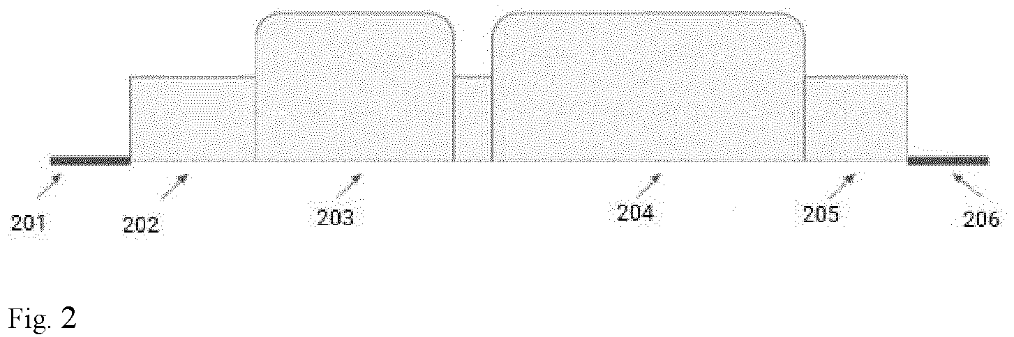
- FIG. 2 the process of surface treatment using atmospheric plasma is shown in FIG. 2 .
- An object to be treated moves towards a reflow soldering device by means of a conveyor device.
- An atmospheric plasma treatment chamber is placed before the reflow soldering device and can provide an atmospheric plasma atmosphere.
- any known plasma generator may be used to provide the atmospheric plasma atmosphere, such as a plasma spray torch or the like.
- a typical plasma spray torch includes a series of nozzles arranged in such a manner that a region to be treated can be ensured to be covered by the plasma atmosphere. The arrangement of the nozzles is freely chosen by those skilled in the art.
- the entire atmospheric plasma treatment system includes transition chambers 202 and 205, an atmospheric plasma treatment chamber 203 and a reflow soldering chamber 204.
- the transition chambers 202 and 205 and the atmospheric plasma treatment chamber 203 need to use an inert gas (such as nitrogen) to replace the air to maintain a required residual oxygen level.
- the atmospheric plasma treatment chamber 203 is equipped with an atmospheric plasma generator, wherein the atmospheric plasma generator is connected to a gas source through a pipeline.
- a reflow soldering process is completed in the reflow soldering chamber 204.
- a specific reflow soldering process may be performed according to a method well known to those skilled in the art, and is not limited in the present application.
- the residual oxygen level (ROL) in the entire working environment of the above-mentioned atmospheric plasma treatment system must be lower than a pre-set value.
- the extent to which residual oxygen levels need to be reduced had not been fully realized. It is expected that the lower the residual oxygen level, the more ideal it is, that is, the closer it is to 0 ppm, the more ideal it is. Therefore, the residual oxygen level needs to be lower than 300 ppm, preferably lower than 200 ppm, more preferably lower than 100 ppm, optimally lower than 50 ppm, even lower than 10 ppm, or even 5 ppm.
- An oxygen analyser is configured in the atmospheric plasma treatment chamber to monitor the residual oxygen level. As an example, a fuel cell oxygen analyser may be used.
- the soldering temperature in the reflow soldering chamber is set to 250°C.
- the sweep speed range of the plasma spray torch may be estimated.
- a sweep speed that is too fast cannot provide sufficient plasma intensity, while a sweep speed that is too slow may result in too high temperatures and too few units per hour (UPH).
- the sweep speed of the plasma spray torch may be between 10 and 250 mm/second.
- the plasma treatment time per unit area should be optimized. Long-term treatment will cause the surface temperature of the DBC to rise sharply and cause re-oxidation. However, short-term treatment cannot remove the oxide film on the DBC surface. Even a thin oxide film may cause soldering failure, which is undesirable.
- solder wettability is an indicator of whether the soldering is good. If there are any firmly attached contaminants (such as oxide films) on the surface to be treated, they will act as a barrier to metal connections and thus hinder surface wettability. Solder spots may not be standard circles, so it is difficult to directly measure the contact angles of the solder spots on the metal surface. The area of solder spots will be used below to evaluate surface wettability. The larger the area of the solder spots and the fuller and more uniform the solder spots are, the better the surface wettability will be.
- the DBC was treated at different sweep speeds and different ROLs, and the solder spot images of FIGS. 3a, 3b and 3c were obtained.
- the ROL in the atmospheric plasma treatment chamber was maintained to be lower than 5 ppm, and the sweep speed of the plasma spray torch was 25 mm/s.
- the ROL in the atmospheric plasma treatment chamber was in the range of approximately 130 to 180 ppm, and the sweep speed of the plasma spray torch was 25 mm/s.
- the ROL in the atmospheric plasma treatment chamber was maintained to be lower than 5 ppm, and the sweep speeds of the plasma spray torch were, from left to right, 150 mm/s, 100 mm/s and 50 mm/s, respectively.
- a lower sweep speed means a longer treatment time and a greater likelihood of achieving good surface wettability.
- the solder spots in FIG. 3b show severe shrinkage. The possible explanation is that due to the higher ROL, the reoxidation process occurred on the treated surface in FIG. 3b .
- the solder spots obtained at a faster sweep speed were uniform and full. It is generally believed that an excessively fast sweep speed will result in insufficient treatment time for the DBC surface.
- the results of the present application show that when the ROL is low enough, since the oxygen is always very thin, the effect of the sweep speed is not obvious.
- the first one is a void ratio, which represents the area of all voids in a target region divided by the area of all solder spots.
- the second indicator is a ratio of solder spots with voids, which represents the number of solder spots with voids divided by the number of all solder spots.
- the inventors compared the void ratios of solder spots after flux soldering and atmospheric plasma treatment.
- the results are shown in Table 1 below.
- the flux model number is SAC305 (purchased from Shanghai Huaqing Welding Materials Technology Co., Ltd.)
- the flux proportion is 0.2% to 5%
- the activity level is ROL0.
- Atmospheric plasma treatment is performed in an atmosphere with a ROL lower than 50 ppm.
- Each group is set with 75 solder spots.
- the solder spots with voids the solder spots with the fewest voids and the solder spots with the most voids are selected as examples, as shown in FIGS. 4a to 4d .
Landscapes
- Engineering & Computer Science (AREA)
- Mechanical Engineering (AREA)
- Physics & Mathematics (AREA)
- Plasma & Fusion (AREA)
- Chemical & Material Sciences (AREA)
- Analytical Chemistry (AREA)
- Electric Connection Of Electric Components To Printed Circuits (AREA)
- Plasma Technology (AREA)
- Treatments Of Macromolecular Shaped Articles (AREA)
Abstract
Disclosed in the present application is a surface treatment method. Atmospheric plasma is provided, and an object to be treated is placed in an atmospheric plasma atmosphere, wherein a residual oxygen level in the atmospheric plasma atmosphere is lower than a pre-set value. A soldering process is integrated into an atmospheric plasma treatment system without any flux protection, and it is ensured that the oxygen level in the atmosphere is reduced to an extremely low level, which can meet the high requirements for surface soldering performance.

Description
- The present application belongs to the field of semiconductor manufacturing. The present application relates to a surface treatment method, and specifically to a method of performing surface cleaning using plasma.
- The manufacturing process of semiconductor elements requires the use of soldering technology. Common objects to be treated are often certain metal materials, and these metal materials are easily oxidized in the presence of oxygen. The oxide film formed after oxidation can lead to bonding defects, such as poor wet spreadability, poor bonding performance, and increased voids. Moreover, once the metal materials melt under high temperature conditions, the oxide film will further become thicker. The thickened oxide film is mixed between bonded objects after bonding, which will cause poor conduction.
- Currently, a commonly used soldering process is flux soldering. Although flux can reduce the surface tension of the object to be treated and remove the oxide film on the surface of the object to be treated, different types of flux still have inevitable disadvantages. One disadvantage of flux soldering is the formation of corrosive flux residue around solder spots, which can lead to long-term reliability issues and is disadvantageous in terms of heat exchange. Another disadvantage of flux soldering is the problem of internal voids. Due to the evaporation and vaporization of flux, internal voids are almost inevitable. In order to reduce internal voids and flux residue, a vacuum reflow oven is used to suck away the flux residue. However, the vacuum process has the following disadvantages: First, some components will degas excessively in the vacuum, and thus a target vacuum pressure needs to be reached very slowly. Second, heat cannot be transferred in the vacuum through convection, but can only be transferred through infra-red radiation or thermal conduction. Third, the price of vacuum equipment is very expensive. For example, according to the quotation of "Torch Technology Co., Ltd", the price of vacuum equipment is 6 to 7 times that of non-vacuum equipment.
- Since soldering requires high soldering activity on the metal surface, the treatment of the metal surface is particularly important. Taking an insulated gate bipolar transistor (IGBT) as an example, it is widely used in many high-power scenarios, such as wind power generation, highspeed rail, electric vehicles, ships, etc. The trend in IGBT applications is towards greater power density, higher switching frequency and smaller volume. Therefore, the reliability of IGBT is crucial. Moreover, the voids that inevitably appear during the soldering process will seriously affect the reliability of the IGBT during operation. A typical IGBT package module is shown in
FIG. 1 . In the figure, 101 represents a primary soldering layer, 102 represents DBC, 103 represents a secondary soldering layer, 104 represents an insulating layer, 105 represents bond copper, and 106 represents a heat dissipation substrate. The main function of the heat dissipation substrate is to quickly transfer the heat generated during the IGBT switching process. The heat dissipation substrate is usually made of copper. The thickness of the heat dissipation substrate is usually 3 to 8 mm. The main function of direct bond copper (DBC) is to ensure the electrical insulation, thermal conductivity and current transmission capabilities between a chip and the heat dissipation substrate. The soldering between the chip and the DBC is referred to as primary soldering. Due to further requirements for heat dissipation, the DBC will be directly soldered on the heat dissipation substrate, which is referred to as secondary soldering. The secondary soldering has a larger soldering area than the primary soldering, and more voids may thus be produced. For some extremely demanding industries such as the new energy field, the individual void ratio of IGBT should be less than 1%, and the overall void ratio should be less than 1.5%. It can be seen that ensuring a stable and low void ratio is an urgent requirement for IGBT module packaging. - In view of this, how to design a new surface treatment method to eliminate the above-mentioned defects and deficiencies in the prior art and realize the high requirements for soldering quality in certain technical fields is an urgent issue for a person skilled in the art to solve.
- The present application relates to a surface treatment method. In particular, the present application relates to an improved method for cleaning a metal surface without using flux and organic solderability preservatives (OSP), so that the object to be treated meets reliability requirements after soldering. This improved method of the present application comprises using atmospheric plasma to treat the metal surface.
- In order to achieve the above-mentioned purpose of the invention, a surface treatment method is disclosed in the present application, comprising steps of: providing atmospheric plasma, and placing an object to be treated in an atmospheric plasma atmosphere, wherein a residual oxygen level in the atmospheric plasma atmosphere is lower than a pre-set value.
- According to another aspect of the present application, the atmospheric plasma is generated by supplying argon, helium, hydrogen, nitrogen, or a combination thereof.
- According to another aspect of the present application, the atmospheric plasma is generated by supplying argon and hydrogen, or nitrogen and hydrogen.
- According to another aspect of the present application, the hydrogen accounts for 1% to 10% of the volume of the atmospheric plasma, and preferably, the hydrogen accounts for 1% to 4% of the volume of the atmospheric plasma.
- According to another aspect of the present application, the pre-set value is 200 ppm, preferably 100 ppm, more preferably 50 ppm, and most preferably 10 ppm.
- According to another aspect of the present application, a surface of the object to be treated is not coated with an organic solderability preservative.
- According to another aspect of the present application, the surface treatment method further comprises a step of: after atmospheric plasma treatment, the object to be treated entering a soldering system, wherein no flux is used in the soldering system.
- According to another aspect of the present application, the atmospheric plasma sweeps the object to be treated at a speed of 10 mm/s to 300 mm/s, preferably 25 mm/s to 150 mm/s, and more preferably 25 mm/s to 100 mm/s.
- According to another aspect of the present application, the treatment method causes a void ratio of a surface of the object to be treated to be less than 1%.
- According to another aspect of the present application, the atmospheric plasma is generated by an atmospheric plasma generator, and the atmospheric plasma generator comprises a plasma spray torch having a series of nozzles arranged in such a manner that the object to be treated can be covered by the atmospheric plasma atmosphere.
- According to another aspect of the present application, the atmospheric plasma is emitted vertically or obliquely to a surface of the object to be treated.
- The technical solution provided by the present application is especially applicable to large-area metal surface soldering in high-demand fields, such as IGBT, and has the following advantages:
- (1) This is an environmentally friendly solution that does not require the use of environmentally unfriendly and health-damaging compounds such as flux and formic acid.
- (2) Plasma treatment leaves no residue, avoiding reliability hazards caused by flux or formic acid residues.
- (3) Plasma treatment of the surface can greatly reduce the void ratio and significantly reduce the internal voids on the metal surface.
- (4) Compared with the vacuum plasma method, the method of the present application allows the process flow to be integrated into the same assembly line without causing interruption of the assembly line. Moreover, the vacuum plasma method requires the DBC and heat dissipation substrate to be placed into the vacuum chamber in batches. This process will inevitably expose the cleaned DBC surface to the oxygen atmosphere, aggravating surface oxidation and causing interruption of the assembly line.
- The advantages and spirit of the present application can be further understood from the following detailed description of the invention and the accompanying drawings.
-
FIG. 1 shows a typical IGBT package module. -
FIG. 2 shows a flow chart of treating a surface with atmospheric plasma in an embodiment of the present application. -
FIGS. 3a, 3b and 3c show schematic diagrams of solder spots on DBC of a plasma spray torch in an embodiment of the present application at different sweep speeds and different ROLs, respectively. -
FIGS. 4a, 4b, 4c and 4d show schematic diagrams of solder spots with voids obtained after flux soldering and atmospheric plasma treatment, respectively. - Specific embodiments of the present application are described in detail below with reference to the accompanying drawings. However, it should be understood that the present application is not limited to the implementations described below, and the technical concept of the present application may be implemented in combination with other well-known techniques or other technologies having the same functions as those well-known techniques.
- In the description of the specific embodiments below, in order to clearly show the structure and manner of operation of the present application, many directional terms will be used for description, but terms such as "front," "rear," "left," "right," "outer," "inner," "outward," "inward," "axial," "radial," etc. should be understood to be terms of convenience rather than restrictive terms.
- In the explanation of particular embodiments below, it must be understood that orientational or positional relationships indicated by terms such as "length," "width," "up," "down," "front," "rear," "left," "right," "vertical," "horizontal," "top", "bottom," "inner" and "outer" are based on the orientational or positional relationships shown in the drawings, and are merely intended to facilitate and simplify the description of the present application, without indicating or implying that the device or element referred to must have a specific orientation or be constructed and operated in a specific orientation, and therefore should not be understood as limiting the present application.
- In addition, the terms "first" and "second" are only used for descriptive purposes rather than limiting chronological order, quantity, or importance, should not be construed as indicating or implying relative importance or implicitly specifying the number of technical features indicated, and are only intended to differentiate one technical feature from another technical feature of the present technical solution. Thus, the features defined with "first" and "second" may explicitly or implicitly include one or more features. In the description of the present application, "multiple" means two or more, unless otherwise expressly and specifically specified. Similarly, a qualifier like "a" appearing herein does not indicate the definition of quantity, but describe a technical feature that has not appeared in the preceding text. Similarly, unless modified by a specific quantity measure word, nouns herein should be regarded as including both singular and plural forms, i.e. the technical solution may include a single one of the technical feature concerned, but may also include a plurality of the technical feature. Similarly, modifiers similar to "approximately" and "about" appearing before numerals herein usually include the numeral, and the specific meaning should be understood in light of the context.
- It should be understood that in the present application, "at least one (item)" means one or more, and "a plurality of" means two or more. The expression "and/or" is used to describe the associative relationship between associated objects, and indicates that three types of relationship may exist; for example, "A and/or B" can mean three situations, namely that A alone is present, B alone is present, and A and B are both present, wherein A and B may be singular or plural. The symbol "/" generally means that the preceding and following associated objects have an "or" relationship. The expression "at least one of the following (items)" or similar means any combination of these items, including a single (item) or any combination of multiple (items). For example, at least one (item) of a, b or c can mean: a, b, c, "a and b," "a and c," "b and c," or "a and b and c", wherein a, b and c may be singular or plural.
- The terms "unit," "member," "object" and "module" described herein indicate units used to process at least one function and operation, and can be implemented by means of hardware components or software components and combinations thereof.
- Unless clearly indicated otherwise, each aspect or embodiment defined herein may be combined with any other aspect(s) or embodiment(s). In particular, any preferred or advantageous feature indicated can be combined with any other preferred or advantageous feature indicated.
- As used herein, plasma, also referred to as electric plasma, is an ionized gas-like substance composed of positive and negative ions produced by ionization of atoms and atomic groups after some electrons have been stripped away. The motion of plasma is mainly dominated by electromagnetic forces and exhibits significant behaviour en masse. Atmospheric plasma refers to electric plasma generated at or near one atmosphere. Both atmospheric plasma and vacuum plasma have high-energy particles, but the atmospheric plasma does not require the provision of a closed reaction chamber and vacuum pumping system like vacuum plasma. Therefore, atmospheric plasma saves a huge vacuum chamber and vacuum pump compared with vacuum plasma, and has an absolute advantage in equipment cost. The surface treatment temperature in the present application may be in the range of about 25°C to about 150°C. The plasma may optionally include at least one gas selected from argon, helium, nitrogen, hydrogen or a combination thereof. In some non-limiting implementations, the hydrogen may account for 1% to 10% of the volume of the atmospheric plasma, preferably about 2% to 8%, and more preferably more than 4% to 7%.
- As used herein, the contact of the atmospheric plasma with a surface to be treated may be accomplished by any suitable means, such as using a plasma jet to sweep the surface. The sweep speed may be varied as needed to target the efficiency required for a specific process. For example, the sweep speed may be in the range of about 1 to about 500 mm/s, such as about 10 to about 300 mm/s, 25 to 300 mm/s, 25 to 250 mm/s, 25 to 150 mm/s, 50 to 150 mm/s , and 50 to 100 mm/s, including all ranges and sub-ranges therebetween.
- Likewise, the length of time that the atmospheric plasma is in contact with the surface to be treated, which may be referred to as residence time, may vary with the sweep speed and the desired surface properties. As a non-limiting example, the residence time may be in the range of 1 second to several minutes, such as about 1 second to about 20 minutes, about 10 seconds to about 10 minutes, about 30 seconds to about 9 minutes, about 1 minute to about 8 minutes, about 2 minutes to about 7 minutes, about 3 minutes to about 6 minutes, or about 4 minutes to about 5 minutes, including all ranges and sub-ranges therebetween.
- As used herein, the device used to generate plasma in the present application may use an OpenAir™ plasma spray torch or an Atomflo™ plasma machine. Specifically, reconstructed treatment parameters can be accurately evaluated according to the sweep speed and the distance from the plasma torch to the surface to be treated.
- As used herein, natural oxidation (NO) refers to exposing the object to be treated to air for two weeks at room temperature to simulate the effect of natural oxidation of the object to be treated during the transfer process.
- As used herein, deep oxidation (DO) refers to placing the DBC cleaned with citric acid in a nitrogen atmosphere of 250°C and 50 ppm for 10 minutes to simulate the surface condition of the DBC after the first soldering during IGBT packaging.
- In an implementation, the atmospheric plasma is generated by supplying argon, helium, hydrogen, nitrogen, or a combination thereof, such as argon and hydrogen, nitrogen and hydrogen, helium and hydrogen, etc.
- As used herein, "clean surface", "surface cleaning", "cleaning" and the like refer to cleaning of organic and inorganic contaminants on the surface to be treated so that more effective and stronger mechanical and electrical connections are produced between metal materials.
- As used herein, solder spot analysis may be performed using X-ray inspection techniques known in the art. X-rays can penetrate inside the package and directly inspect the quality of solder spots.
- The following embodiments take the treatment of contaminants and oxide films on a DBC surface during the IGBT packaging process as an example. In a nitrogen atmosphere, this embodiment uses atmospheric plasma to treat the DBC surface instead of other chemical methods.
- A solder used in flux soldering is Sn305, and its melting point is 217°C.
- Because the surface of DBC is usually copper, that is easily oxidised. An organic solderability preservative is a common protection means in the prior art. The OSP is a layer of organic copper complex film grown on the surface of copper by using a chemical method. Although the OSP is cheap and has good solderability initially, after being used for a period of time, its solderability deteriorates significantly, its shelf life is insufficient, and it is prone to surface dis-colouration, uneven film thickness, excessive film thickness (too thick or too thin), and other issues. If there is a hole in the OSP just on the copper surface, the copper surface will start to oxidise from the hole, resulting in poor assembly. Moreover, the thicker the OSP, the better it protects the copper foil. However, correspondingly, it also requires a more active flux to remove the OSP.
- In this embodiment, on the premise that the surface of the DBC is not coated with any organic solderability preservative while no flux is used, atmospheric plasma is used to perform surface treatment of the obj ect to be treated, and the requirements for wet spreadability and void ratio are reached.
- In this embodiment, the process of surface treatment using atmospheric plasma is shown in
FIG. 2 . An object to be treated moves towards a reflow soldering device by means of a conveyor device. An atmospheric plasma treatment chamber is placed before the reflow soldering device and can provide an atmospheric plasma atmosphere. Here, any known plasma generator may be used to provide the atmospheric plasma atmosphere, such as a plasma spray torch or the like. A typical plasma spray torch includes a series of nozzles arranged in such a manner that a region to be treated can be ensured to be covered by the plasma atmosphere. The arrangement of the nozzles is freely chosen by those skilled in the art. - As shown in
FIG. 2 , 201 and 206 represent carrying platforms for placing and fixing the object to be treated. The entire atmospheric plasma treatment system includestransition chambers plasma treatment chamber 203 and areflow soldering chamber 204. Among them, thetransition chambers plasma treatment chamber 203 need to use an inert gas (such as nitrogen) to replace the air to maintain a required residual oxygen level. The atmosphericplasma treatment chamber 203 is equipped with an atmospheric plasma generator, wherein the atmospheric plasma generator is connected to a gas source through a pipeline. A reflow soldering process is completed in thereflow soldering chamber 204. A specific reflow soldering process may be performed according to a method well known to those skilled in the art, and is not limited in the present application. - The atmospheric plasma generator in the atmospheric
plasma treatment chamber 203 can generate any gas suitable for surface treatment, such as nitrogen, argon, helium or their mixtures with hydrogen. - It was unexpectedly discovered that the residual oxygen level (ROL) in the entire working environment of the above-mentioned atmospheric plasma treatment system must be lower than a pre-set value. In previous studies, the extent to which residual oxygen levels need to be reduced had not been fully realized. It is expected that the lower the residual oxygen level, the more ideal it is, that is, the closer it is to 0 ppm, the more ideal it is. Therefore, the residual oxygen level needs to be lower than 300 ppm, preferably lower than 200 ppm, more preferably lower than 100 ppm, optimally lower than 50 ppm, even lower than 10 ppm, or even 5 ppm. An oxygen analyser is configured in the atmospheric plasma treatment chamber to monitor the residual oxygen level. As an example, a fuel cell oxygen analyser may be used.
- As an example, a nitrogen atmosphere may be utilized to protect the entire work environment. Initially, the atmosphere of the working environment is replaced with nitrogen. After the ROL is reduced to about 200 ppm, the ROL may be quickly reduced to, for example, 10 ppm or less by continuing to use nitrogen for replacement or using the combustion of the hydrogen-containing plasma to consume the remaining oxygen.
- In this embodiment, the soldering temperature in the reflow soldering chamber is set to 250°C.
- The sweep speed range of the plasma spray torch may be estimated. A sweep speed that is too fast cannot provide sufficient plasma intensity, while a sweep speed that is too slow may result in too high temperatures and too few units per hour (UPH). As an example, the sweep speed of the plasma spray torch may be between 10 and 250 mm/second. In other words, the plasma treatment time per unit area (inversely proportional to the sweep speed) should be optimized. Long-term treatment will cause the surface temperature of the DBC to rise sharply and cause re-oxidation. However, short-term treatment cannot remove the oxide film on the DBC surface. Even a thin oxide film may cause soldering failure, which is undesirable.
- Surface wettability is an indicator of whether the soldering is good. If there are any firmly attached contaminants (such as oxide films) on the surface to be treated, they will act as a barrier to metal connections and thus hinder surface wettability. Solder spots may not be standard circles, so it is difficult to directly measure the contact angles of the solder spots on the metal surface. The area of solder spots will be used below to evaluate surface wettability. The larger the area of the solder spots and the fuller and more uniform the solder spots are, the better the surface wettability will be.
- According to the process shown in
FIG. 2 , the DBC was treated at different sweep speeds and different ROLs, and the solder spot images ofFIGS. 3a, 3b and 3c were obtained. As shown inFIG. 3a , the ROL in the atmospheric plasma treatment chamber was maintained to be lower than 5 ppm, and the sweep speed of the plasma spray torch was 25 mm/s. InFIG. 3b , the ROL in the atmospheric plasma treatment chamber was in the range of approximately 130 to 180 ppm, and the sweep speed of the plasma spray torch was 25 mm/s. InFIG. 3c , the ROL in the atmospheric plasma treatment chamber was maintained to be lower than 5 ppm, and the sweep speeds of the plasma spray torch were, from left to right, 150 mm/s, 100 mm/s and 50 mm/s, respectively. - A lower sweep speed means a longer treatment time and a greater likelihood of achieving good surface wettability. However, the solder spots in
FIG. 3b show severe shrinkage. The possible explanation is that due to the higher ROL, the reoxidation process occurred on the treated surface inFIG. 3b . Unexpectedly, as shown inFIG. 3c , the solder spots obtained at a faster sweep speed were uniform and full. It is generally believed that an excessively fast sweep speed will result in insufficient treatment time for the DBC surface. However, the results of the present application show that when the ROL is low enough, since the oxygen is always very thin, the effect of the sweep speed is not obvious. - Internal voids are another important evaluation criterion for whether the soldering is good. The following two indicators will be considered. The first one is a void ratio, which represents the area of all voids in a target region divided by the area of all solder spots. The second indicator is a ratio of solder spots with voids, which represents the number of solder spots with voids divided by the number of all solder spots.
- To this end, using deeply oxidised DBC as a soldering base material, the inventors compared the void ratios of solder spots after flux soldering and atmospheric plasma treatment. The results are shown in Table 1 below. In flux soldering, the flux model number is SAC305 (purchased from Shanghai Huaqing Welding Materials Technology Co., Ltd.), the flux proportion is 0.2% to 5%, and the activity level is ROL0. Atmospheric plasma treatment is performed in an atmosphere with a ROL lower than 50 ppm. Each group is set with 75 solder spots. Among the solder spots with voids, the solder spots with the fewest voids and the solder spots with the most voids are selected as examples, as shown in
FIGS. 4a to 4d .Table 1 Solder spots with the fewest voids Solder spots with the most voids Ratio of solder spots with voids Void ratio Flux soldering FIG. 4b FIG. 4a 100% 2.7% OpenAir FIG. 4d FIG. 4c 14.76% 0.95% - Table 1 shows that compared with flux soldering, atmospheric plasma treatment can significantly reduce the void ratio and ratio of solder spots with voids. After flux soldering, 100% of the solder spots had voids, and the average void ratio was 2.7%. However, the DBC treated with atmospheric plasma had a greatly reduced void ratio, and the quality of solder spots was higher.
- Therefore, plasma treatment showed better performance not only in terms of the void ratio but also in terms of the number of voided solder spots. This means that flux soldering can lead to a rapid increase of voids if the soldering area is increased, which is not the case with atmospheric plasma treatment. The present application provides a new surface treatment method. The soldering process is integrated into the atmospheric plasma treatment system without any flux protection, and it is ensured that the oxygen level in the atmosphere is reduced to an extremely low level, which can meet the high requirements for surface soldering performance.
- Described in the description are merely preferred specific embodiments of the present application, and the above embodiments are merely used to explain the technical solution of the present application without limiting the present application. All technical solutions obtainable by those skilled in the art by logical analysis, reasoning or limited experiment according to the concept of the present application should be within the scope of the present application.
Claims (10)
- A surface treatment method, characterised by comprising steps of: providing atmospheric plasma, and placing an object to be treated in an atmospheric plasma atmosphere, wherein a residual oxygen level in the atmospheric plasma atmosphere is lower than a pre-set value.
- The surface treatment method according to claim 1, characterised in that the atmospheric plasma is generated by supplying argon, helium, hydrogen, nitrogen, or a combination thereof.
- The surface treatment method according to claim 2, characterised in that the atmospheric plasma is generated by supplying argon and hydrogen, or nitrogen and hydrogen.
- The surface treatment method according to claim 3, characterised in that the hydrogen accounts for 1% to 10% of the volume of the atmospheric plasma, and preferably, the hydrogen accounts for 1% to 4% of the volume of the atmospheric plasma.
- The surface treatment method according to any one of claims 1-4, characterised in that the pre-set value is 200 ppm, preferably 100 ppm, more preferably 50 ppm, and most preferably 10 ppm.
- The surface treatment method according to any one of claims 1-4, characterised in that a surface of the object to be treated is not coated with an organic solderability preservative.
- The surface treatment method according to any one of claims 1-4, characterised by further comprising a step of: after atmospheric plasma treatment, the object to be treated entering a soldering system, wherein no flux is used in the soldering system.
- The surface treatment method according to any one of claims 1-4, characterised in that the atmospheric plasma sweeps the object to be treated at a speed of 10 mm/s to 300 mm/s, preferably 25 mm/s to 150 mm/s, and more preferably 25 mm/s to 100 mm/s.
- The surface treatment method according to any one of claims 1-4, characterised in that a void ratio of a surface of the object to be treated is less than 1%.
- The surface treatment method according to any one of claims 1-4, characterised in that the atmospheric plasma is emitted vertically or obliquely to a surface of the object to be treated.
Applications Claiming Priority (1)
| Application Number | Priority Date | Filing Date | Title |
|---|---|---|---|
| CN202311221379.4A CN117276086A (en) | 2023-09-20 | 2023-09-20 | a surface treatment method |
Publications (1)
| Publication Number | Publication Date |
|---|---|
| EP4528784A1 true EP4528784A1 (en) | 2025-03-26 |
Family
ID=89200264
Family Applications (1)
| Application Number | Title | Priority Date | Filing Date |
|---|---|---|---|
| EP24199415.1A Pending EP4528784A1 (en) | 2023-09-20 | 2024-09-10 | Surface treatment method |
Country Status (5)
| Country | Link |
|---|---|
| US (1) | US12678879B2 (en) |
| EP (1) | EP4528784A1 (en) |
| JP (1) | JP7843321B2 (en) |
| CN (1) | CN117276086A (en) |
| TW (1) | TWI925238B (en) |
Families Citing this family (1)
| Publication number | Priority date | Publication date | Assignee | Title |
|---|---|---|---|---|
| CN117276086A (en) * | 2023-09-20 | 2023-12-22 | 液化空气(中国)投资有限公司 | a surface treatment method |
Citations (4)
| Publication number | Priority date | Publication date | Assignee | Title |
|---|---|---|---|---|
| WO2002103770A1 (en) * | 2001-06-15 | 2002-12-27 | Sem Technology Co., Ltd. | Apparatus and method for cleaning the surface of a substrate |
| CN103065987A (en) * | 2011-10-24 | 2013-04-24 | 株式会社日立高新技术仪器 | Chip engagement device and chip engagement method |
| JP2014075406A (en) * | 2012-10-03 | 2014-04-24 | Hitachi High-Tech Instruments Co Ltd | Die bonder device and die bonding method |
| US20150072473A1 (en) * | 2013-09-11 | 2015-03-12 | Kui Kam Lam | Die attachment apparatus and method utilizing activated forming gas |
Family Cites Families (25)
| Publication number | Priority date | Publication date | Assignee | Title |
|---|---|---|---|---|
| US4921157A (en) * | 1989-03-15 | 1990-05-01 | Microelectronics Center Of North Carolina | Fluxless soldering process |
| DE4032328A1 (en) * | 1989-11-06 | 1991-09-19 | Wls Karl Heinz Grasmann Weichl | METHOD AND DEVICE FOR PROCESSING JOINT PARTNERS TO BE SOLDERED |
| DE4041270A1 (en) * | 1990-12-21 | 1992-06-25 | Grasmann Karl Heinz Wls | METHOD AND DEVICE FOR THE PROCESSING OF ELECTRONIC FLAT ASSEMBLIES, ESPECIALLY WITH CIRCUIT BOARDS |
| US6021940A (en) * | 1993-12-15 | 2000-02-08 | L'air Liquide, Societe Anonyme Pour L'etude Et L'exploitation Des Procedes Georges Claude | Method and apparatus for reflow soldering metallic surfaces |
| US5609290A (en) * | 1995-04-20 | 1997-03-11 | The University Of North Carolina At Charlotte | Fluxless soldering method |
| WO1997019204A1 (en) * | 1995-11-07 | 1997-05-29 | Seiko Epson Corporation | Method and apparatus for surface treatment |
| JP3116792B2 (en) * | 1995-11-24 | 2000-12-11 | 松下電器産業株式会社 | Plasma cleaning device and plasma cleaning method |
| KR100473432B1 (en) * | 1998-09-17 | 2005-03-08 | 가부시키가이샤 다무라 세이사쿠쇼 | Bump forming method, soldering preprocessing method, soldering method, soldering preprocessing apparatus and soldering apparatus |
| US6742701B2 (en) * | 1998-09-17 | 2004-06-01 | Kabushiki Kaisha Tamura Seisakusho | Bump forming method, presoldering treatment method, soldering method, bump forming apparatus, presoldering treatment device and soldering apparatus |
| WO2001041963A2 (en) * | 1999-12-01 | 2001-06-14 | L'Air Liquide Societe Anonyme à Directoire et Conseil de Surveillance pour l'Etude et l'Exploitation des Procedes Georges Claude | Systems and methods for application of atmospheric plasma surface treatment to various electronic component packaging and assembly methods |
| US6468833B2 (en) * | 2000-03-31 | 2002-10-22 | American Air Liquide, Inc. | Systems and methods for application of substantially dry atmospheric plasma surface treatment to various electronic component packaging and assembly methods |
| JP2002001253A (en) * | 2000-06-27 | 2002-01-08 | Matsushita Electric Works Ltd | Plasma cleaning apparatus, plasma cleaning method, soldering system and soldering method |
| JP2002050860A (en) * | 2000-08-04 | 2002-02-15 | Toray Eng Co Ltd | Mounting method and mounting device |
| JP4688423B2 (en) * | 2004-02-27 | 2011-05-25 | 独立行政法人物質・材料研究機構 | Laser welding method |
| DE102007013326A1 (en) * | 2007-03-20 | 2008-09-25 | Linde Ag | Apparatus and method for pre-treatment of electronic components before soldering |
| JP2011023509A (en) * | 2009-07-15 | 2011-02-03 | Renesas Electronics Corp | Method for manufacturing semiconductor device, and semiconductor manufacturing apparatus used in the same |
| JP5666246B2 (en) * | 2010-10-29 | 2015-02-12 | 株式会社日立ハイテクインスツルメンツ | Die bonder apparatus and die bonder method |
| US8844793B2 (en) * | 2010-11-05 | 2014-09-30 | Raytheon Company | Reducing formation of oxide on solder |
| JP2014165347A (en) * | 2013-02-25 | 2014-09-08 | Sumitomo Electric Printed Circuit Inc | Printed wiring board, electric component, and manufacturing method of printed wiring board |
| US10032609B1 (en) * | 2013-12-18 | 2018-07-24 | Surfx Technologies Llc | Low temperature atmospheric pressure plasma applications |
| US11170980B2 (en) * | 2017-10-27 | 2021-11-09 | Corning Incorporated | Methods of treating a surface of a polymer material by atmospheric pressure plasma |
| TW202030768A (en) * | 2018-09-04 | 2020-08-16 | 美商瑟菲克斯科技股份有限公司 | Device and method for plasma treatment of electronic materials |
| CN114951148B (en) * | 2022-05-11 | 2023-10-17 | 珠海方正科技多层电路板有限公司 | Method for cleaning printed circuit board |
| CN116160101A (en) * | 2023-03-10 | 2023-05-26 | 西安交通大学 | Plasma welding method for metal sheet and metal sheet |
| CN117276086A (en) * | 2023-09-20 | 2023-12-22 | 液化空气(中国)投资有限公司 | a surface treatment method |
-
2023
- 2023-09-20 CN CN202311221379.4A patent/CN117276086A/en active Pending
-
2024
- 2024-08-31 JP JP2024150396A patent/JP7843321B2/en active Active
- 2024-09-02 TW TW113133054A patent/TWI925238B/en active
- 2024-09-10 EP EP24199415.1A patent/EP4528784A1/en active Pending
- 2024-09-20 US US18/890,961 patent/US12678879B2/en active Active
Patent Citations (4)
| Publication number | Priority date | Publication date | Assignee | Title |
|---|---|---|---|---|
| WO2002103770A1 (en) * | 2001-06-15 | 2002-12-27 | Sem Technology Co., Ltd. | Apparatus and method for cleaning the surface of a substrate |
| CN103065987A (en) * | 2011-10-24 | 2013-04-24 | 株式会社日立高新技术仪器 | Chip engagement device and chip engagement method |
| JP2014075406A (en) * | 2012-10-03 | 2014-04-24 | Hitachi High-Tech Instruments Co Ltd | Die bonder device and die bonding method |
| US20150072473A1 (en) * | 2013-09-11 | 2015-03-12 | Kui Kam Lam | Die attachment apparatus and method utilizing activated forming gas |
Also Published As
| Publication number | Publication date |
|---|---|
| CN117276086A (en) | 2023-12-22 |
| US20250091148A1 (en) | 2025-03-20 |
| JP7843321B2 (en) | 2026-04-09 |
| US12678879B2 (en) | 2026-07-14 |
| JP2025048763A (en) | 2025-04-03 |
| TWI925238B (en) | 2026-05-11 |
| TW202513201A (en) | 2025-04-01 |
Similar Documents
| Publication | Publication Date | Title |
|---|---|---|
| US8283783B2 (en) | Solder material, method for manufacturing the same, joined body, method for manufacturing the same, power semiconductor module, and method for manufacturing the same | |
| US6905063B2 (en) | Method of manufacturing semiconductor device | |
| US11396059B2 (en) | Copper/ceramic bonded body, insulating circuit substrate, copper/ceramic bonded body production method, and insulating circuit substrate production method | |
| US12037294B2 (en) | Copper/ceramic bonded body, insulating circuit substrate, copper/ceramic bonded body production method, and insulating circuit substrate production method | |
| CN108511407B (en) | Thermal interface material and preparation method and application method thereof | |
| US12002732B2 (en) | Copper/ceramic assembly, insulated circuit board, method for producing copper/ceramic assembly, and method for producing insulated circuit board | |
| US20250091148A1 (en) | Surface treatment method | |
| US11460254B2 (en) | Heat pipe and method for manufacturing heat pipe | |
| US20220415846A1 (en) | Interconnect structure for semiconductor with ultra-fine pitch and forming method thereof | |
| US8944310B2 (en) | Method of manufacturing a semiconductor device | |
| JP2002001253A (en) | Plasma cleaning apparatus, plasma cleaning method, soldering system and soldering method | |
| US20210238103A1 (en) | Copper/ceramic bonded body, insulating circuit substrate, copper/ceramic bonded body production method, and insulating circuit substrate production method | |
| US20230328898A1 (en) | Board | |
| CN221125886U (en) | Electron beam window structure and electron beam sterilization apparatus including the same | |
| JP2001184956A (en) | Superconducting wire manufacturing method | |
| CN114561623A (en) | Surface treatment method for bismuth telluride material | |
| CN109877411A (en) | Microcircuit Soldering Assembly Method Without Flux | |
| KR100243374B1 (en) | Manufacturing method of semiconductor lead frame | |
| JP2024104424A (en) | Fixed anode X-ray tube | |
| CN117340490A (en) | A microwave plasma-assisted eutectic reflow soldering method | |
| CN118016517A (en) | A method for removing oxides and seeping soldering flux around a chip | |
| CN117080049A (en) | Electron beam window structure and electron beam sterilization device including the same | |
| KR920001675B1 (en) | Superconducting Goods | |
| TW202415205A (en) | Electronic device and method of manufacturing the same | |
| CN119824405A (en) | Silicon wafer cutting surface passivation process and device |
Legal Events
| Date | Code | Title | Description |
|---|---|---|---|
| PUAI | Public reference made under article 153(3) epc to a published international application that has entered the european phase |
Free format text: ORIGINAL CODE: 0009012 |
|
| STAA | Information on the status of an ep patent application or granted ep patent |
Free format text: STATUS: THE APPLICATION HAS BEEN PUBLISHED |
|
| AK | Designated contracting states |
Kind code of ref document: A1 Designated state(s): AL AT BE BG CH CY CZ DE DK EE ES FI FR GB GR HR HU IE IS IT LI LT LU LV MC ME MK MT NL NO PL PT RO RS SE SI SK SM TR |
|
| STAA | Information on the status of an ep patent application or granted ep patent |
Free format text: STATUS: REQUEST FOR EXAMINATION WAS MADE |
|
| 17P | Request for examination filed |
Effective date: 20250926 |