EP4525561A1 - Bridging a selv barrier of an isolated driver - Google Patents
Bridging a selv barrier of an isolated driver Download PDFInfo
- Publication number
- EP4525561A1 EP4525561A1 EP23197828.9A EP23197828A EP4525561A1 EP 4525561 A1 EP4525561 A1 EP 4525561A1 EP 23197828 A EP23197828 A EP 23197828A EP 4525561 A1 EP4525561 A1 EP 4525561A1
- Authority
- EP
- European Patent Office
- Prior art keywords
- printed circuit
- circuit board
- capacitor
- layer
- isolated
- Prior art date
- Legal status (The legal status is an assumption and is not a legal conclusion. Google has not performed a legal analysis and makes no representation as to the accuracy of the status listed.)
- Pending
Links
Images


Classifications
-
- H—ELECTRICITY
- H05—ELECTRIC TECHNIQUES NOT OTHERWISE PROVIDED FOR
- H05K—PRINTED CIRCUITS; CASINGS OR CONSTRUCTIONAL DETAILS OF ELECTRIC APPARATUS; MANUFACTURE OF ASSEMBLAGES OF ELECTRICAL COMPONENTS
- H05K1/00—Printed circuits
- H05K1/16—Printed circuits incorporating printed electric components, e.g. printed resistors, capacitors or inductors
- H05K1/162—Printed circuits incorporating printed electric components, e.g. printed resistors, capacitors or inductors incorporating printed capacitors
-
- H—ELECTRICITY
- H05—ELECTRIC TECHNIQUES NOT OTHERWISE PROVIDED FOR
- H05K—PRINTED CIRCUITS; CASINGS OR CONSTRUCTIONAL DETAILS OF ELECTRIC APPARATUS; MANUFACTURE OF ASSEMBLAGES OF ELECTRICAL COMPONENTS
- H05K1/00—Printed circuits
- H05K1/02—Details
- H05K1/0213—Electrical arrangements not otherwise provided for
- H05K1/0254—High voltage adaptations; Electrical insulation details; Overvoltage or electrostatic discharge protection ; Arrangements for regulating voltages or for using plural voltages
- H05K1/0256—Electrical insulation details, e.g. around high voltage areas
-
- H—ELECTRICITY
- H05—ELECTRIC TECHNIQUES NOT OTHERWISE PROVIDED FOR
- H05K—PRINTED CIRCUITS; CASINGS OR CONSTRUCTIONAL DETAILS OF ELECTRIC APPARATUS; MANUFACTURE OF ASSEMBLAGES OF ELECTRICAL COMPONENTS
- H05K1/00—Printed circuits
- H05K1/02—Details
- H05K1/14—Structural association of two or more printed circuits
- H05K1/144—Stacked arrangements of planar printed circuit boards
-
- H—ELECTRICITY
- H05—ELECTRIC TECHNIQUES NOT OTHERWISE PROVIDED FOR
- H05K—PRINTED CIRCUITS; CASINGS OR CONSTRUCTIONAL DETAILS OF ELECTRIC APPARATUS; MANUFACTURE OF ASSEMBLAGES OF ELECTRICAL COMPONENTS
- H05K2201/00—Indexing scheme relating to printed circuits covered by H05K1/00
- H05K2201/01—Dielectrics
- H05K2201/0137—Materials
- H05K2201/0179—Thin film deposited insulating layer, e.g. inorganic layer for printed capacitor
-
- H—ELECTRICITY
- H05—ELECTRIC TECHNIQUES NOT OTHERWISE PROVIDED FOR
- H05K—PRINTED CIRCUITS; CASINGS OR CONSTRUCTIONAL DETAILS OF ELECTRIC APPARATUS; MANUFACTURE OF ASSEMBLAGES OF ELECTRICAL COMPONENTS
- H05K2201/00—Indexing scheme relating to printed circuits covered by H05K1/00
- H05K2201/01—Dielectrics
- H05K2201/0183—Dielectric layers
- H05K2201/0187—Dielectric layers with regions of different dielectrics in the same layer, e.g. in a printed capacitor for locally changing the dielectric properties
-
- H—ELECTRICITY
- H05—ELECTRIC TECHNIQUES NOT OTHERWISE PROVIDED FOR
- H05K—PRINTED CIRCUITS; CASINGS OR CONSTRUCTIONAL DETAILS OF ELECTRIC APPARATUS; MANUFACTURE OF ASSEMBLAGES OF ELECTRICAL COMPONENTS
- H05K2201/00—Indexing scheme relating to printed circuits covered by H05K1/00
- H05K2201/04—Assemblies of printed circuits
- H05K2201/041—Stacked PCBs, i.e. having neither an empty space nor mounted components in between
-
- H—ELECTRICITY
- H05—ELECTRIC TECHNIQUES NOT OTHERWISE PROVIDED FOR
- H05K—PRINTED CIRCUITS; CASINGS OR CONSTRUCTIONAL DETAILS OF ELECTRIC APPARATUS; MANUFACTURE OF ASSEMBLAGES OF ELECTRICAL COMPONENTS
- H05K2201/00—Indexing scheme relating to printed circuits covered by H05K1/00
- H05K2201/07—Electric details
- H05K2201/0753—Insulation
- H05K2201/0761—Insulation resistance, e.g. of the surface of the PCB between the conductors
-
- H—ELECTRICITY
- H05—ELECTRIC TECHNIQUES NOT OTHERWISE PROVIDED FOR
- H05K—PRINTED CIRCUITS; CASINGS OR CONSTRUCTIONAL DETAILS OF ELECTRIC APPARATUS; MANUFACTURE OF ASSEMBLAGES OF ELECTRICAL COMPONENTS
- H05K2201/00—Indexing scheme relating to printed circuits covered by H05K1/00
- H05K2201/09—Shape and layout
- H05K2201/09818—Shape or layout details not covered by a single group of H05K2201/09009 - H05K2201/09809
- H05K2201/09972—Partitioned, e.g. portions of a PCB dedicated to different functions; Boundary lines therefore; Portions of a PCB being processed separately or differently
-
- H—ELECTRICITY
- H05—ELECTRIC TECHNIQUES NOT OTHERWISE PROVIDED FOR
- H05K—PRINTED CIRCUITS; CASINGS OR CONSTRUCTIONAL DETAILS OF ELECTRIC APPARATUS; MANUFACTURE OF ASSEMBLAGES OF ELECTRICAL COMPONENTS
- H05K2201/00—Indexing scheme relating to printed circuits covered by H05K1/00
- H05K2201/10—Details of components or other objects attached to or integrated in a printed circuit board
- H05K2201/10007—Types of components
- H05K2201/10106—Light emitting diode [LED]
-
- H—ELECTRICITY
- H05—ELECTRIC TECHNIQUES NOT OTHERWISE PROVIDED FOR
- H05K—PRINTED CIRCUITS; CASINGS OR CONSTRUCTIONAL DETAILS OF ELECTRIC APPARATUS; MANUFACTURE OF ASSEMBLAGES OF ELECTRICAL COMPONENTS
- H05K3/00—Apparatus or processes for manufacturing printed circuits
- H05K3/36—Assembling printed circuits with other printed circuits
- H05K3/368—Assembling printed circuits with other printed circuits parallel to each other
Definitions
- the present invention relates to bridging a SELV (safety extra-low voltage) barrier of an isolated driver especially in the sense of communicating a signal across the SELV barrier.
- the present invention relates to a SELV barrier for an isolated driver, especially an isolated LED driver, an isolated driver, especially an isolated LED driver, comprising such a SELV barrier, and a use of a metallized or metallic surface in an electronic component-carrying printed circuit board of an isolated driver, especially an isolated LED driver.
- a SELV barrier for an isolated driver, especially an isolated LED driver, an isolated driver, especially an isolated LED driver, comprising such a SELV barrier, and a use of a metallized or metallic surface in an electronic component-carrying printed circuit board of an isolated driver, especially an isolated LED driver in order to allow for communicating a signal across such a SELV barrier in a particularly efficient and reliable manner.
- a SELV barrier for an isolated driver especially an isolated LED driver, an isolated driver, especially an isolated LED driver, comprising such a SELV barrier, and a use of a metallized or metallic surface in an electronic component-carrying printed circuit board of an isolated driver, especially an isolated LED driver, thereby allowing for communicating a signal across such a SELV barrier in a particularly efficient and reliable manner.
- a SELV barrier for an isolated driver especially an isolated LED driver
- Said SELV barrier comprises at least one capacitor for communicating a signal across the SELV barrier.
- the corresponding electrodes of the at least one capacitor are implemented as metallized or metallic surfaces in one printed circuit board or a plurality of superimposed printed circuit boards.
- a signal can be communicated across the SELV barrier in a particularly efficient and reliable manner.
- the at least one capacitor comprises or is at least one Y-class capacitor.
- efficiency can further be increased.
- the corresponding electrodes of the at least one capacitor are isolated against each other preferably with the aid of the respective isolating material, especially the respective resin material, of the printed circuit board or of the plurality of superimposed printed circuit boards.
- the isolating material or the resin material can be the respective printed circuit board base material, thereby reducing complexity, which leads to reduced costs.
- the printed circuit board comprises or is a multi-layer printed circuit board.
- flexibility can be increased, thereby reducing inefficiencies.
- the at least one capacitor can efficiently be implemented.
- the primary printed circuit board comprises or is a single-layer primary printed circuit board or a multi-layer primary printed circuit board.
- the secondary printed circuit board comprises or is a single-layer secondary printed circuit board or a multi-layer secondary printed circuit board.
- the primary printed circuit board comprises a first one of the corresponding electrodes of the at least one capacitor. Additionally or alternatively, the secondary printed circuit board comprises at least a second one of the corresponding electrodes of the at least one capacitor.
- the secondary printed circuit board is directly arranged on the primary printed circuit board.
- the secondary printed circuit board is arranged on the primary printed circuit board such that the secondary printed circuit board is separated from the primary printed circuit board by air, especially an air gap, and/or a foil, especially an isolating foil, and/or solder resist.
- At least a part or each of the metallized or metallic surfaces comprises or is made of copper.
- efficiency can further be increased.
- a distance between the metallized or metallic surfaces is between 0.3 millimeters and 1.7 millimeters, preferably between 0.5 millimeters and 1.5 millimeters, more preferably between 0.8 millimeters and 1.2 millimeters, most preferably between 0.9 millimeters and 1.1 millimeters.
- reliability can further be increased.
- an isolated driver especially an isolated LED driver, comprising a SELV barrier according to the first aspect of the present invention or any of its implementation forms, respectively, is provided.
- a signal can be communicated across the SELV barrier in a particularly efficient and reliable manner. Further advantageously, not only space can be saved but also a longer life of the corresponding circuit can be achieved because fewer components can have a defect.
- a use of a metallized or metallic surface in an electronic component-carrying printed circuit board of an isolated driver, especially an isolated LED driver, as one electrode of at least one capacitor, preferably at least one Y-class capacitor, of the isolated driver, especially the isolated LED driver, is provided.
- the at least one capacitor preferably the at least one Y-class capacitor, is adapted for communicating a signal across a SELV barrier of the isolated driver, especially the isolated LED driver.
- the signal can be communicated across the SELV barrier in a particularly efficient and reliable manner.
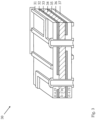
- a first exemplary embodiment of a SELV barrier 10 for an isolated driver comprises at least one capacitor, exemplarily an integrated capacitor 11, for communicating a signal across the SELV barrier 10.
- the corresponding electrodes 11a, 11b of the at least one capacitor or the integrated capacitor 11, respectively are implemented as metallized or metallic surfaces in one printed circuit board or a plurality of superimposed printed circuit boards, exemplarily in the printed circuit board 12.
- the printed circuit board 12 exemplarily comprises two layers, namely a first layer 12a and a second layer 12b.
- the first layer 12a of the multi-layer, especially the two-layer, printed circuit board 12 comprises the first one 11a of the corresponding electrodes 11a, 11b of the at least one capacitor or the integrated capacitor 11, respectively.
- the second layer 12b of the multi-layer, especially the two-layer, printed circuit board 12 comprises the second one 11b of the corresponding electrodes 11a, 11b of the at least one capacitor or the integrated capacitor 11, respectively.
- the at least one capacitor or the integrated capacitor 11, respectively comprises or is at least one Y-class capacitor or a Y-class capacitor, respectively.
- the corresponding electrodes 11a, 11b of the at least one capacitor or the integrated capacitor 11 are isolated against each other preferably with the aid of the respective isolating material, especially the respective resin material, of the printed circuit board or of the plurality of superimposed printed circuit boards, exemplarily of the printed circuit board 12
- the isolating material or said resin material can especially be understood to be the respective printed circuit board base material.
- the isolating material, especially the resin material, or said printed circuit board base material comprises or is FR4 material.
- the at least one capacitor or the integrated capacitor 11 is implemented as a plate capacitor or any kind thereof.
- corresponding electrodes 11a, 11b or the metallized or metallic surfaces respectively, it is noted that it might be particularly advantageous if at least a part or each of the corresponding electrodes 11a, 11b or the metallized or metallic surfaces, respectively, comprises or is made of copper.
- a distance, exemplarily equipped with reference sign 13 in Fig. 1 , between the corresponding electrodes 11a, 11b or the metallized or metallic surfaces, respectively, may especially be between 0.3 millimeters and 1.7 millimeters, preferably between 0.5 millimeters and 1.5 millimeters, more preferably between 0.8 millimeters and 1.2 millimeters, most preferably between 0.9 millimeters and 1.1 millimeters.
- the at least one capacitor is a single capacitor such as the integrated capacitor 11 according to Fig. 1 , it might be particularly advantageous if said distance 13 is 1 millimeter or between 0.95 millimeters and 1.05 millimeters, preferably between 0.98 millimeters and 1.02 millimeters.
- said distance 13 may preferably be between 0.1 millimeters and 0.7 millimeters or between 0.1 millimeters and 0.3 millimeters.
- a second exemplary embodiment of a SELV barrier 20 is shown in combination with an isolated driver, especially an isolated LED driver.
- the isolated driver or the isolated LED driver exemplarily comprises a transformer 25, a mains terminal 26, a multitude of components 27, especially electronic components, and LED connectors 28.
- a plurality of superimposed printed circuit boards exemplarily the two superimposed printed circuit boards 22a, 22b, is used.
- Said two superimposed printed circuit boards 22a, 22b exemplarily comprise a primary printed circuit board or the main printed circuit board 22a, respectively, and a secondary printed circuit board or the sub-print 22b, respectively.
- connections 24 especially electrical connections, between the primary printed circuit board or the main printed circuit board 22a, respectively, and the secondary printed circuit board or the sub-print 22b, respectively.
- the SELV barrier 20 of Fig. 2 for an isolated driver comprises at least one capacitor, exemplarily the capacitor 21, for communicating a signal across the SELV barrier 20.
- the corresponding electrodes 21a, 21b of the at least one capacitor or the capacitor 21, respectively are implemented as metallized or metallic surfaces in the plurality of superimposed printed circuit boards, exemplarily in the two superimposed printed circuit boards 22a, 22b.
- the primary printed circuit board or the main printed circuit board 22a can comprise or be a single-layer printed circuit board or a multi-layer printed circuit board.
- the primary printed circuit board or the main printed circuit board 22a comprises the first one 21a of the corresponding electrodes 21a, 21b of the at least one capacitor or the capacitor 21, respectively.
- the primary printed circuit board or the main printed circuit board 22a comprises or is a multi-layer printed circuit board
- an inner layer of the multi-layer printed circuit board comprises the first one 21a of the corresponding electrodes 21a, 21b especially for a multi-layer printed circuit board with at least three layers or a most distant layer of the multi-layer printed circuit board with respect to the secondary printed circuit board or the sub-print 22b, respectively, comprises the first one 21a of the corresponding electrodes 21a, 21b especially for a multi-layer printed circuit board with two or at least two layers.
- the secondary printed circuit board or the sub-print 22b can comprise or be a single-layer printed circuit board or a multi-layer printed circuit board.
- the secondary printed circuit board or the sub-print 22b comprises the second one 21b of the corresponding electrodes 21a, 21b of the at least one capacitor or the capacitor 21, respectively.
- the secondary printed circuit board or the sub-print 22b comprises or is a multi-layer printed circuit board
- an inner layer of the multi-layer printed circuit board comprises the second one 21b of the corresponding electrodes 21a, 21b especially for a multi-layer printed circuit board with at least three layers or a most distant layer of the multi-layer printed circuit board with respect to the primary printed circuit board or the main printed circuit board 22a, respectively, comprises the second one 21b of the corresponding electrodes 21a, 21b especially for a multi-layer printed circuit board with two or at least two layers.
- the secondary printed circuit board or the sub-print 22b is exemplarily arranged at a defined distance from the primary printed circuit board or the main printed circuit board, respectively, especially from the first one 21a of the corresponding electrodes 21a, 21b of the at least one capacitor, exemplarily the capacitor 21, or the respective one of the corresponding metallized or metallic surfaces located on the primary printed circuit board or the main printed circuit board 22a, respectively.
- the secondary printed circuit board or the sub-print 22b is arranged on the primary printed circuit board or the main printed circuit board 22a, respectively, such that the secondary printed circuit board or the sub-print 22b, respectively, is separated from the primary printed circuit board or the main printed circuit board 22a, respectively, by solder resist and air especially in addition to respective printed circuit board base material, preferably FR4 material.
- the secondary printed circuit board or the sub-print 22b can directly be arranged on the primary printed circuit board or the main printed circuit board 22a, respectively.
- Fig. 3 illustrates an exemplary layer structure of a multi-layer printed circuit board 30 as mentioned in the context of Fig. 1 or Fig. 2 , respectively.
- said multi-layer printed circuit board 30 comprises four layers 31, 33, 35, 37.
- the first layer 31 and the fourth layer 37 are the outer layers
- the second layer 33 and the third layer 35 are the inner layers.
- At least one or each of the four layers 31, 33, 35, 37 comprises a thickness between 30 micrometers and 40 micrometers, especially 35 micrometers.
- At least one or each of the four layers 31, 33, 35, 37 comprises or is made of copper.
- first layer 31 and the second layer 33 are separated by a first prepreg layer 32 with a thickness between 0.8 millimeters and 0.14 millimeters, preferably a thickness of 0.11 millimeters.
- the third layer 35 and the fourth layer 37 are separated by a second prepreg layer 36 with a thickness between 0.8 millimeters and 0.14 millimeters, preferably a thickness of 0.11 millimeters.
- each pair of the inner layers 33, 35 and the corresponding outer layers 31, 37 are separated by a respective prepreg layer 32, 36 with a thickness between 0.8 millimeters and 0.14 millimeters, preferably a thickness of 0.11 millimeters.
- the second layer 33 and the third layer 35 or the inner layers, respectively, are separated by a core layer 34 with a thickness between 1.07 millimeters and 1.19 millimeters, preferably a thickness of 1.13 millimeters.
- the corresponding relative permittivity of the first prepreg layer 32 or the second prepreg layer 36, respectively is between 4 and 4.5, preferably between 4.1 and 4.4, more preferably between 4.2 and 4.3, most preferably 4.29.
- the corresponding relative permittivity of the core layer 34 is between 3.6 and 4.2, preferably between 3.8 and 4.1, more preferably between 3.9 and 4, most preferably 3.96.
- the corresponding relative permittivity of the first prepreg layer 32 and/or the corresponding relative permittivity of the second prepreg layer 36 is between 1.03 times and 1.13 times, preferably between 1.05 times and 1.11 times, more preferably between 1.07 times and 1.09 times, most preferably 1.08 times, the corresponding relative permittivity of the core layer 34.
- the printed circuit board 30 comprises a thickness between 1.395 millimeters and 1.705 millimeters, preferably between 1.45 millimeters and 1.65 millimeters, more preferably between 1.5 millimeters and 1.6 millimeters, most preferably of 1.55 millimeters.
Landscapes
- Engineering & Computer Science (AREA)
- Microelectronics & Electronic Packaging (AREA)
- Structure Of Printed Boards (AREA)
- Parts Printed On Printed Circuit Boards (AREA)
Abstract
A SELV barrier (10) for an isolated driver, especially an isolated LED driver, is provided. Said SELV barrier (10) comprises at least one capacitor (11) for communicating a signal across the SELV barrier (10). In this context, the corresponding electrodes (11a, 11b) of the at least one capacitor (11) are implemented as metallized or metallic surfaces in one printed circuit board (12) or a plurality of superimposed printed circuit boards.
Description
- The present invention relates to bridging a SELV (safety extra-low voltage) barrier of an isolated driver especially in the sense of communicating a signal across the SELV barrier. In particular, the present invention relates to a SELV barrier for an isolated driver, especially an isolated LED driver, an isolated driver, especially an isolated LED driver, comprising such a SELV barrier, and a use of a metallized or metallic surface in an electronic component-carrying printed circuit board of an isolated driver, especially an isolated LED driver.
- Generally, in times of an increasing number of applications employing isolated drivers with a SELV barrier, such as LED lighting applications, there is a growing need of a SELV barrier for an isolated driver, especially an isolated LED driver, an isolated driver, especially an isolated LED driver, comprising such a SELV barrier, and a use of a metallized or metallic surface in an electronic component-carrying printed circuit board of an isolated driver, especially an isolated LED driver in order to allow for communicating a signal across such a SELV barrier in a particularly efficient and reliable manner.
- Accordingly, there is the object to provide a SELV barrier for an isolated driver, especially an isolated LED driver, an isolated driver, especially an isolated LED driver, comprising such a SELV barrier, and a use of a metallized or metallic surface in an electronic component-carrying printed circuit board of an isolated driver, especially an isolated LED driver, thereby allowing for communicating a signal across such a SELV barrier in a particularly efficient and reliable manner.
- This object is solved by the features of the first independent claim for a SELV barrier for an isolated driver, especially an isolated LED driver, the features of the second independent claim for an isolated driver, especially an isolated LED driver, comprising such a SELV barrier, and the features of the third independent claim for a use of a metallized or metallic surface in an electronic component-carrying printed circuit board of an isolated driver, especially an isolated LED driver. The dependent claims contain further developments.
- According to a first aspect of the present invention, a SELV barrier for an isolated driver, especially an isolated LED driver, is provided. Said SELV barrier comprises at least one capacitor for communicating a signal across the SELV barrier. In this context, the corresponding electrodes of the at least one capacitor are implemented as metallized or metallic surfaces in one printed circuit board or a plurality of superimposed printed circuit boards.
- Advantageously, a signal can be communicated across the SELV barrier in a particularly efficient and reliable manner.
- Further advantageously, not only space can be saved but also a longer life of the corresponding circuit can be achieved because fewer components can have a defect.
- As a further advantage, especially in the context of the isolated driver or the isolated LED driver, respectively, not only feedback signals can be transferred from a secondary side to a primary side but also gate actuations can be performed on the secondary side starting from the primary side.
- According to an implementation form of the first aspect of the present invention, the at least one capacitor comprises or is at least one Y-class capacitor.
- Advantageously, for instance, efficiency can further be increased.
- According to a further implementation form of the first aspect of the present invention, the corresponding electrodes of the at least one capacitor are isolated against each other preferably with the aid of the respective isolating material, especially the respective resin material, of the printed circuit board or of the plurality of superimposed printed circuit boards.
- Advantageously, for example, the isolating material or the resin material can be the respective printed circuit board base material, thereby reducing complexity, which leads to reduced costs.
- According to a further implementation form of the first aspect of the present invention, the printed circuit board comprises or is a multi-layer printed circuit board.
- Advantageously, for instance, flexibility can be increased, thereby reducing inefficiencies.
- According to a further implementation form of the first aspect of the present invention, a first layer of the multi-layer printed circuit board comprises a first one of the corresponding electrodes of the at least one capacitor. Additionally or alternatively, at least a second layer of the multi-layer printed circuit board comprises at least a second one of the corresponding electrodes of the at least one capacitor.
- Advantageously, for example, the at least one capacitor can efficiently be implemented.
- According to a further implementation form of the first aspect of the present invention, the plurality of superimposed printed circuit boards comprises or is at least or exactly a primary printed circuit board and a secondary printed circuit board.
- Advantageously, for instance, the corresponding dielectric strength of the at least one capacitor can efficiently be increased.
- According to a further implementation form of the first aspect of the present invention, the primary printed circuit board comprises or is a single-layer primary printed circuit board or a multi-layer primary printed circuit board. Additionally or alternatively, the secondary printed circuit board comprises or is a single-layer secondary printed circuit board or a multi-layer secondary printed circuit board.
- Advantageously, for example, complexity can further be reduced, thereby increasing cost-efficiency.
- According to a further implementation form of the first aspect of the present invention, the primary printed circuit board comprises a first one of the corresponding electrodes of the at least one capacitor. Additionally or alternatively, the secondary printed circuit board comprises at least a second one of the corresponding electrodes of the at least one capacitor.
- Advantageously, for instance, a desired dielectric strength of the at least one capacitor can efficiently be adjusted.
- According to a further implementation form of the first aspect of the present invention, the secondary printed circuit board is arranged at a defined distance from the primary printed circuit board, especially from the respective one of the corresponding electrodes of the at least one capacitor or the respective one of the corresponding metallized or metallic surfaces located on the primary printed circuit board.
- Advantageously, for example, a desired capacitance of the at least one capacitor can efficiently be adjusted.
- According to a further implementation form of the first aspect of the present invention, the secondary printed circuit board is directly arranged on the primary printed circuit board. Alternatively, the secondary printed circuit board is arranged on the primary printed circuit board such that the secondary printed circuit board is separated from the primary printed circuit board by air, especially an air gap, and/or a foil, especially an isolating foil, and/or solder resist.
- Advantageously, for instance, the corresponding dielectric strength of the at least one capacitor can be increased in an efficient manner.
- According to a further implementation form of the first aspect of the present invention, at least a part or each of the metallized or metallic surfaces comprises or is made of copper.
- Advantageously, for example, efficiency can further be increased.
- According to a further implementation form of the first aspect of the present invention, a distance between the metallized or metallic surfaces is between 0.3 millimeters and 1.7 millimeters, preferably between 0.5 millimeters and 1.5 millimeters, more preferably between 0.8 millimeters and 1.2 millimeters, most preferably between 0.9 millimeters and 1.1 millimeters.
- Advantageously, for instance, reliability can further be increased.
- According to a second aspect of the present invention, an isolated driver, especially an isolated LED driver, comprising a SELV barrier according to the first aspect of the present invention or any of its implementation forms, respectively, is provided.
- Advantageously, a signal can be communicated across the SELV barrier in a particularly efficient and reliable manner. Further advantageously, not only space can be saved but also a longer life of the corresponding circuit can be achieved because fewer components can have a defect.
- As a further advantage, not only feedback signals can be transferred from a secondary side to a primary side but also gate actuations can be performed on the secondary side starting from the primary side.
- According to a third aspect of the present invention, a use of a metallized or metallic surface in an electronic component-carrying printed circuit board of an isolated driver, especially an isolated LED driver, as one electrode of at least one capacitor, preferably at least one Y-class capacitor, of the isolated driver, especially the isolated LED driver, is provided.
- Advantageously, not only space can be saved but also a longer life of the corresponding circuit can be achieved because fewer components can have a defect.
- According to an implementation form of the third aspect of the present invention, the at least one capacitor, preferably the at least one Y-class capacitor, is adapted for communicating a signal across a SELV barrier of the isolated driver, especially the isolated LED driver.
- Advantageously, the signal can be communicated across the SELV barrier in a particularly efficient and reliable manner.
- Further advantageously, not only feedback signals can be transferred from a secondary side to a primary side but also gate actuations can be performed on the secondary side starting from the primary side.
- Exemplary embodiments of the invention are now further explained with respect to the drawings by way of example only, and not for limitation. In the drawings:
- Fig. 1
- shows a first exemplary embodiment of a SELV barrier;
- Fig. 2
- shows a second exemplary embodiment of a SELV barrier in combination with an isolated driver, especially an isolated LED driver; and
- Fig. 3
- shows an exemplary layer structure of a printed circuit board for a SELV barrier.
- In accordance with
Fig. 1 , especially illustrating a view of a cross-section of a printedcircuit board 12, a first exemplary embodiment of aSELV barrier 10 for an isolated driver, especially an isolated LED driver, comprises at least one capacitor, exemplarily an integratedcapacitor 11, for communicating a signal across theSELV barrier 10. - In this context, the
corresponding electrodes capacitor 11, respectively, are implemented as metallized or metallic surfaces in one printed circuit board or a plurality of superimposed printed circuit boards, exemplarily in the printedcircuit board 12. - As it can further be seen from
Fig. 1 , the printedcircuit board 12 exemplarily comprises two layers, namely afirst layer 12a and asecond layer 12b. - Further exemplarily, the
first layer 12a of the multi-layer, especially the two-layer, printedcircuit board 12 comprises the first one 11a of thecorresponding electrodes capacitor 11, respectively. Furthermore, thesecond layer 12b of the multi-layer, especially the two-layer, printedcircuit board 12 comprises the second one 11b of thecorresponding electrodes capacitor 11, respectively. - It is noted that it might be particularly advantageous if the at least one capacitor or the integrated
capacitor 11, respectively, comprises or is at least one Y-class capacitor or a Y-class capacitor, respectively. - It is further noted that the
corresponding electrodes capacitor 11 are isolated against each other preferably with the aid of the respective isolating material, especially the respective resin material, of the printed circuit board or of the plurality of superimposed printed circuit boards, exemplarily of the printedcircuit board 12 - With respect to said isolating material or said resin material, respectively, it is noted that the isolating material or the resin material, respectively, can especially be understood to be the respective printed circuit board base material.
- It might be particularly advantageous if the isolating material, especially the resin material, or said printed circuit board base material comprises or is FR4 material.
- With respect to the at least one capacitor or the integrated
capacitor 11, respectively, it is noted that it might be particularly advantageous if the at least one capacitor or the integratedcapacitor 11, respectively, is implemented as a plate capacitor or any kind thereof. - Moreover, with respect to the corresponding
electrodes corresponding electrodes - Furthermore, a distance, exemplarily equipped with
reference sign 13 inFig. 1 , between thecorresponding electrodes - In this context, especially for the case that the at least one capacitor is a single capacitor such as the
integrated capacitor 11 according toFig. 1 , it might be particularly advantageous if saiddistance 13 is 1 millimeter or between 0.95 millimeters and 1.05 millimeters, preferably between 0.98 millimeters and 1.02 millimeters. - Otherwise, especially for the case that the at least one capacitor is a parallel connection and/or a series connection of multiple capacitors, said
distance 13 may preferably be between 0.1 millimeters and 0.7 millimeters or between 0.1 millimeters and 0.3 millimeters. - Now, with respect to
Fig. 2 , especially depicting a correspondingtop view 201 and a corresponding view of across-section 202, a second exemplary embodiment of aSELV barrier 20 is shown in combination with an isolated driver, especially an isolated LED driver. - As it can be seen from said
Fig. 2 , the isolated driver or the isolated LED driver, respectively, exemplarily comprises atransformer 25, a mains terminal 26, a multitude ofcomponents 27, especially electronic components, andLED connectors 28. - As mentioned in the context of
Fig. 1 , especially as an alternative to the single printedcircuit board 12 ofFig. 1 , in this exemplary case according toFig. 2 , a plurality of superimposed printed circuit boards, exemplarily the two superimposed printedcircuit boards - Said two superimposed printed
circuit boards circuit board 22a, respectively, and a secondary printed circuit board or the sub-print 22b, respectively. - As it can further be seen from
Fig. 2 , there areconnections 24, especially electrical connections, between the primary printed circuit board or the main printedcircuit board 22a, respectively, and the secondary printed circuit board or the sub-print 22b, respectively. - For the sake of completeness, it is noted that further secondary printed circuit boards or at least one further sub-print, respectively, can be used.
- By analogy with the
SELV barrier 10 according toFig. 1 , theSELV barrier 20 ofFig. 2 for an isolated driver, especially an isolated LED driver, comprises at least one capacitor, exemplarily thecapacitor 21, for communicating a signal across theSELV barrier 20. - In this context, the corresponding
electrodes capacitor 21, respectively, are implemented as metallized or metallic surfaces in the plurality of superimposed printed circuit boards, exemplarily in the two superimposed printedcircuit boards - It is noted that all the explanations above regarding the
capacitor 11 ofFig. 1 can analogously apply for thecapacitor 21 ofFig. 2 , and vice versa. - With respect to the primary printed circuit board or the main printed
circuit board 22a, respectively, it is noted that the primary printed circuit board or the main printedcircuit board 22a, respectively, can comprise or be a single-layer printed circuit board or a multi-layer printed circuit board. - Exemplarily, the primary printed circuit board or the main printed
circuit board 22a, respectively, comprises the first one 21a of thecorresponding electrodes capacitor 21, respectively. - Especially in the case that the primary printed circuit board or the main printed
circuit board 22a, respectively, comprises or is a multi-layer printed circuit board, it might be particularly advantageous if an inner layer of the multi-layer printed circuit board comprises the first one 21a of thecorresponding electrodes corresponding electrodes - With respect the secondary printed circuit board or the sub-print 22b, respectively, it is noted that the secondary printed circuit board or the sub-print 22b, respectively, can comprise or be a single-layer printed circuit board or a multi-layer printed circuit board.
- Exemplarily, the secondary printed circuit board or the sub-print 22b, respectively, comprises the second one 21b of the
corresponding electrodes capacitor 21, respectively. - Especially in the case that the secondary printed circuit board or the sub-print 22b, respectively, comprises or is a multi-layer printed circuit board, it might be particularly advantageous if an inner layer of the multi-layer printed circuit board comprises the second one 21b of the
corresponding electrodes circuit board 22a, respectively, comprises the second one 21b of thecorresponding electrodes - It is further noted that the secondary printed circuit board or the sub-print 22b, respectively, is exemplarily arranged at a defined distance from the primary printed circuit board or the main printed circuit board, respectively, especially from the first one 21a of the
corresponding electrodes capacitor 21, or the respective one of the corresponding metallized or metallic surfaces located on the primary printed circuit board or the main printedcircuit board 22a, respectively. - Moreover, in this exemplary case of
Fig. 2 , the secondary printed circuit board or the sub-print 22b, respectively, is arranged on the primary printed circuit board or the main printedcircuit board 22a, respectively, such that the secondary printed circuit board or the sub-print 22b, respectively, is separated from the primary printed circuit board or the main printedcircuit board 22a, respectively, by solder resist and air especially in addition to respective printed circuit board base material, preferably FR4 material. - Especially as an alternative thereto, it is noted that the secondary printed circuit board or the sub-print 22b, respectively, can directly be arranged on the primary printed circuit board or the main printed
circuit board 22a, respectively. - It is further noted that all the explanations above regarding the metallized or metallic surfaces of
Fig. 1 can analogously apply for the metallized or metallic surfaces ofFig. 2 , and vice versa. - Finally,
Fig. 3 illustrates an exemplary layer structure of a multi-layer printedcircuit board 30 as mentioned in the context ofFig. 1 orFig. 2 , respectively. - Exemplarily, as it can be seen from
Fig. 3 , said multi-layer printedcircuit board 30 comprises fourlayers first layer 31 and the fourth layer 37 are the outer layers, whereas thesecond layer 33 and thethird layer 35 are the inner layers. - In this context, at least one or each of the four
layers - Preferably, at least one or each of the four
layers - Furthermore, the
first layer 31 and thesecond layer 33 are separated by afirst prepreg layer 32 with a thickness between 0.8 millimeters and 0.14 millimeters, preferably a thickness of 0.11 millimeters. Thethird layer 35 and the fourth layer 37 are separated by a second prepreg layer 36 with a thickness between 0.8 millimeters and 0.14 millimeters, preferably a thickness of 0.11 millimeters. Accordingly, each pair of theinner layers outer layers 31, 37 are separated by arespective prepreg layer 32, 36 with a thickness between 0.8 millimeters and 0.14 millimeters, preferably a thickness of 0.11 millimeters. - Moreover, the
second layer 33 and thethird layer 35 or the inner layers, respectively, are separated by acore layer 34 with a thickness between 1.07 millimeters and 1.19 millimeters, preferably a thickness of 1.13 millimeters. - With respect to at least one or each of the prepreg layers 32 and 36, it is noted that it might be particularly advantageous if the corresponding relative permittivity of the
first prepreg layer 32 or the second prepreg layer 36, respectively, is between 4 and 4.5, preferably between 4.1 and 4.4, more preferably between 4.2 and 4.3, most preferably 4.29. - With respect to the
core layer 34, it is noted that it might be particularly advantageous if the corresponding relative permittivity of thecore layer 34 is between 3.6 and 4.2, preferably between 3.8 and 4.1, more preferably between 3.9 and 4, most preferably 3.96. - It is further noted that it might be particularly advantageous if the corresponding relative permittivity of the
first prepreg layer 32 and/or the corresponding relative permittivity of the second prepreg layer 36 is between 1.03 times and 1.13 times, preferably between 1.05 times and 1.11 times, more preferably between 1.07 times and 1.09 times, most preferably 1.08 times, the corresponding relative permittivity of thecore layer 34. - With respect to the printed
circuit board 30, it is noted that it might be particularly advantageous if the printedcircuit board 30 comprises a thickness between 1.395 millimeters and 1.705 millimeters, preferably between 1.45 millimeters and 1.65 millimeters, more preferably between 1.5 millimeters and 1.6 millimeters, most preferably of 1.55 millimeters. - While various embodiments of the present invention have been described above, it should be understood that they have been presented by way of example only, and not limitation. Numerous changes to the disclosed embodiments can be made in accordance with the disclosure herein without departing from the spirit or scope of the invention. Thus, the breadth and scope of the present invention should not be limited by any of the above described embodiments. Rather, the scope of the invention should be defined in accordance with the following claims and their equivalents.
- Although the invention has been illustrated and described with respect to one or more implementations, equivalent alterations and modifications will occur to others skilled in the art upon the reading and understanding of this specification and the annexed drawings. In addition, while a particular feature of the invention may have been disclosed with respect to only one of several implementations, such feature may be combined with one or more other features of the other implementations as may be desired and advantageous for any given or particular application.
Claims (15)
- A SELV barrier (10, 20) for an isolated driver, especially an isolated LED driver, comprising:
at least one capacitor (11, 21) for communicating a signal across the SELV barrier (10, 20),
wherein the corresponding electrodes (11a, 11b, 21a, 21b) of the at least one capacitor (11, 21) are implemented as metallized or metallic surfaces in one printed circuit board (12) or a plurality of superimposed printed circuit boards (22a, 22b). - The SELV barrier (10, 20) according to claim 1,
wherein the at least one capacitor (11, 21) comprises or is at least one Y-class capacitor. - The SELV barrier (10, 20) according to claim 1 or 2,
wherein the corresponding electrodes (11a, 11b, 21a, 21b) of the at least one capacitor (11, 21) are isolated against each other preferably with the aid of the respective isolating material, especially the respective resin material, of the printed circuit board (12) or of the plurality of superimposed printed circuit boards (22a, 22b) . - The SELV barrier (10, 20) according to any of the claims 1 to 3,
wherein the printed circuit board (12) comprises or is a multi-layer printed circuit board (12, 30). - The SELV (10, 20) barrier according to claim 4,
wherein a first layer (12a) of the multi-layer printed circuit board (12) comprises a first one (11a) of the corresponding electrodes (11a, 11b) of the at least one capacitor (11), and/or
wherein at least a second layer (12b) of the multi-layer printed circuit board (12) comprises at least a second one (11b) of the corresponding electrodes (11a, 11b) of the at least one capacitor (11). - The SELV barrier (10, 20) according to any of the claims 1 to 5,
wherein the plurality of superimposed printed circuit boards (22a, 22b) comprises or is at least or exactly a primary printed circuit board (22a) and a secondary printed circuit board (22b). - The SELV barrier (10, 20) according to claim 6,wherein the primary printed circuit board (22a) comprises or is a single-layer primary printed circuit board or a multi-layer primary printed circuit board, and/orwherein the secondary printed circuit board (22b) comprises or is a single-layer secondary printed circuit board or a multi-layer secondary printed circuit board.
- The SELV barrier (10, 20) according to claim 6 or 7,wherein the primary printed circuit board (22a) comprises a first one (21a) of the corresponding electrodes (21a, 21b) of the at least one capacitor (21), and/orwherein the secondary printed circuit board (22b) comprises at least a second one (21b) of the corresponding electrodes (21a, 21b) of the at least one capacitor (21).
- The SELV barrier (10, 20) according to any of the claims 6 to 8,
wherein the secondary printed circuit board (22b) is arranged at a defined distance from the primary printed circuit board (22a), especially from the respective one of the corresponding electrodes (21a, 21b) of the at least one capacitor (21) or the respective one of the corresponding metallized or metallic surfaces located on the primary printed circuit board (22a). - The SELV barrier (10, 20) according to any of the claims 6 to 9,wherein the secondary printed circuit board (22b) is directly arranged on the primary printed circuit board (22a), orwherein the secondary printed circuit board (22b) is arranged on the primary printed circuit board (22a) such that the secondary printed circuit board (22b) is separated from the primary printed circuit board (22a) by air, especially an air gap, and/or a foil, especially an isolating foil, and/or solder resist (23).
- The SELV barrier (10, 20) according to any of the claims 1 to 10,
wherein at least a part or each of the metallized or metallic surfaces comprises or is made of copper. - The SELV barrier (10, 20) according to any of the claims 1 to 11,
wherein a distance (13) between the metallized or metallic surfaces is between 0.3 millimeters and 1.7 millimeters, preferably between 0.5 millimeters and 1.5 millimeters, more preferably between 0.8 millimeters and 1.2 millimeters, most preferably between 0.9 millimeters and 1.1 millimeters. - An isolated driver, especially an isolated LED driver, comprising a SELV barrier (10, 20) according to any of the claims 1 to 12.
- A use of a metallized or metallic surface in an electronic component-carrying printed circuit board (12, 22a, 22b) of an isolated driver, especially an isolated LED driver, as one electrode (11a, 11b, 21a, 21b) of at least one capacitor (11, 21), preferably at least one Y-class capacitor, of the isolated driver, especially the isolated LED driver.
- The use according to claim 14,
wherein the at least one capacitor (11, 21), preferably the at least one Y-class capacitor, is adapted for communicating a signal across a SELV barrier (10, 20) of the isolated driver, especially the isolated LED driver.
Priority Applications (2)
| Application Number | Priority Date | Filing Date | Title |
|---|---|---|---|
| EP23197828.9A EP4525561A1 (en) | 2023-09-18 | 2023-09-18 | Bridging a selv barrier of an isolated driver |
| PCT/EP2024/075121 WO2025061507A1 (en) | 2023-09-18 | 2024-09-09 | Bridging a selv barrier of an isolated driver |
Applications Claiming Priority (1)
| Application Number | Priority Date | Filing Date | Title |
|---|---|---|---|
| EP23197828.9A EP4525561A1 (en) | 2023-09-18 | 2023-09-18 | Bridging a selv barrier of an isolated driver |
Publications (1)
| Publication Number | Publication Date |
|---|---|
| EP4525561A1 true EP4525561A1 (en) | 2025-03-19 |
Family
ID=88093706
Family Applications (1)
| Application Number | Title | Priority Date | Filing Date |
|---|---|---|---|
| EP23197828.9A Pending EP4525561A1 (en) | 2023-09-18 | 2023-09-18 | Bridging a selv barrier of an isolated driver |
Country Status (2)
| Country | Link |
|---|---|
| EP (1) | EP4525561A1 (en) |
| WO (1) | WO2025061507A1 (en) |
Citations (4)
| Publication number | Priority date | Publication date | Assignee | Title |
|---|---|---|---|---|
| US20060044733A1 (en) * | 2004-09-01 | 2006-03-02 | Wkk Distribution, Ltd. | Buried capacitors for multi-layer printed circuit boards |
| GB2474476A (en) * | 2009-10-15 | 2011-04-20 | Gigle Semiconductor Ltd | An isolating capacitor using a PCB layer as a dielectric |
| US20120230074A1 (en) * | 2009-09-24 | 2012-09-13 | Iain Barnett | Electrical isolators |
| WO2022243169A1 (en) * | 2021-05-21 | 2022-11-24 | Signify Holding B.V. | Esd protection of chip scale package leds |
-
2023
- 2023-09-18 EP EP23197828.9A patent/EP4525561A1/en active Pending
-
2024
- 2024-09-09 WO PCT/EP2024/075121 patent/WO2025061507A1/en not_active Ceased
Patent Citations (4)
| Publication number | Priority date | Publication date | Assignee | Title |
|---|---|---|---|---|
| US20060044733A1 (en) * | 2004-09-01 | 2006-03-02 | Wkk Distribution, Ltd. | Buried capacitors for multi-layer printed circuit boards |
| US20120230074A1 (en) * | 2009-09-24 | 2012-09-13 | Iain Barnett | Electrical isolators |
| GB2474476A (en) * | 2009-10-15 | 2011-04-20 | Gigle Semiconductor Ltd | An isolating capacitor using a PCB layer as a dielectric |
| WO2022243169A1 (en) * | 2021-05-21 | 2022-11-24 | Signify Holding B.V. | Esd protection of chip scale package leds |
Also Published As
| Publication number | Publication date |
|---|---|
| WO2025061507A1 (en) | 2025-03-27 |
Similar Documents
| Publication | Publication Date | Title |
|---|---|---|
| US20080223603A1 (en) | Capacitor embedded printed circuit board | |
| US10217558B2 (en) | Embedded magnetic component transformer device | |
| US7843303B2 (en) | Multilayer inductor | |
| US20140225702A1 (en) | Multilayer inductor and power supply circuit module | |
| US20070001796A1 (en) | Printed circuit board with integrated inductor | |
| JP2009503777A (en) | LIGHTING DEVICE HAVING SEALING UNIT WITH INTEGRATED DRIVE CIRCUIT | |
| US10264676B2 (en) | Passive element array and printed wiring board | |
| US8035309B2 (en) | Light emitting device | |
| US20100117777A1 (en) | Transformer | |
| CN1392756A (en) | Flexible conductive foil with electronic circuit | |
| US9204545B2 (en) | Multilayer substrate | |
| CN114513892B (en) | Power conversion module | |
| WO2025061507A1 (en) | Bridging a selv barrier of an isolated driver | |
| US7035082B2 (en) | Structure of multi-electrode capacitor and method for manufacturing process of the same | |
| US6922129B2 (en) | High-work-efficiency multilayered circuit board | |
| KR100798287B1 (en) | Multilayer capacitor | |
| CN204425772U (en) | Multilager base plate | |
| US20100238605A1 (en) | Multilayer chip capacitor and method of fabricating the same | |
| EP2670212B1 (en) | A half bridge induction heating generator and a capacitor assembly for a half bridge induction heating generator | |
| US7871892B2 (en) | Method for fabricating buried capacitor structure | |
| WO2021009865A1 (en) | High-density multilayer substrate and method for manufacturing same | |
| CN110418492B (en) | Substrate | |
| KR20200028622A (en) | Device for reducing noise | |
| WO2011132476A1 (en) | Electronic component with laminated substrate | |
| KR100528013B1 (en) | Printed Circuit Boards with Capacitors |
Legal Events
| Date | Code | Title | Description |
|---|---|---|---|
| PUAI | Public reference made under article 153(3) epc to a published international application that has entered the european phase |
Free format text: ORIGINAL CODE: 0009012 |
|
| STAA | Information on the status of an ep patent application or granted ep patent |
Free format text: STATUS: THE APPLICATION HAS BEEN PUBLISHED |
|
| AK | Designated contracting states |
Kind code of ref document: A1 Designated state(s): AL AT BE BG CH CY CZ DE DK EE ES FI FR GB GR HR HU IE IS IT LI LT LU LV MC ME MK MT NL NO PL PT RO RS SE SI SK SM TR |
|
| STAA | Information on the status of an ep patent application or granted ep patent |
Free format text: STATUS: REQUEST FOR EXAMINATION WAS MADE |
|
| 17P | Request for examination filed |
Effective date: 20250519 |