EP4525304A1 - Polyphase filter circuitry - Google Patents
Polyphase filter circuitry Download PDFInfo
- Publication number
- EP4525304A1 EP4525304A1 EP23197554.1A EP23197554A EP4525304A1 EP 4525304 A1 EP4525304 A1 EP 4525304A1 EP 23197554 A EP23197554 A EP 23197554A EP 4525304 A1 EP4525304 A1 EP 4525304A1
- Authority
- EP
- European Patent Office
- Prior art keywords
- source
- ppf
- circuitry
- capacitor
- circuit
- Prior art date
- Legal status (The legal status is an assumption and is not a legal conclusion. Google has not performed a legal analysis and makes no representation as to the accuracy of the status listed.)
- Pending
Links
Images






Classifications
-
- H—ELECTRICITY
- H03—ELECTRONIC CIRCUITRY
- H03H—IMPEDANCE NETWORKS, e.g. RESONANT CIRCUITS; RESONATORS
- H03H11/00—Networks using active elements
- H03H11/02—Multiple-port networks
- H03H11/16—Networks for phase shifting
- H03H11/18—Two-port phase shifters providing a predetermined phase shift, e.g. "all-pass" filters
-
- H—ELECTRICITY
- H03—ELECTRONIC CIRCUITRY
- H03H—IMPEDANCE NETWORKS, e.g. RESONANT CIRCUITS; RESONATORS
- H03H17/00—Networks using digital techniques
- H03H17/02—Frequency selective networks
- H03H17/0248—Filters characterised by a particular frequency response or filtering method
- H03H17/0264—Filter sets with mutual related characteristics
- H03H17/0273—Polyphase filters
- H03H17/0275—Polyphase filters comprising non-recursive filters
-
- H—ELECTRICITY
- H03—ELECTRONIC CIRCUITRY
- H03F—AMPLIFIERS
- H03F3/00—Amplifiers with only discharge tubes or only semiconductor devices as amplifying elements
- H03F3/189—High-frequency amplifiers, e.g. radio frequency amplifiers
- H03F3/19—High-frequency amplifiers, e.g. radio frequency amplifiers with semiconductor devices only
- H03F3/193—High-frequency amplifiers, e.g. radio frequency amplifiers with semiconductor devices only with field-effect devices
- H03F3/1935—High-frequency amplifiers, e.g. radio frequency amplifiers with semiconductor devices only with field-effect devices with junction-FET devices
-
- H—ELECTRICITY
- H03—ELECTRONIC CIRCUITRY
- H03F—AMPLIFIERS
- H03F3/00—Amplifiers with only discharge tubes or only semiconductor devices as amplifying elements
- H03F3/26—Push-pull amplifiers; Phase-splitters therefor
- H03F3/265—Push-pull amplifiers; Phase-splitters therefor with field-effect transistors only
-
- H—ELECTRICITY
- H03—ELECTRONIC CIRCUITRY
- H03F—AMPLIFIERS
- H03F3/00—Amplifiers with only discharge tubes or only semiconductor devices as amplifying elements
- H03F3/50—Amplifiers in which input is applied to, or output is derived from, an impedance common to input and output circuits of the amplifying element, e.g. cathode follower
- H03F3/505—Amplifiers in which input is applied to, or output is derived from, an impedance common to input and output circuits of the amplifying element, e.g. cathode follower with field-effect devices
-
- H—ELECTRICITY
- H03—ELECTRONIC CIRCUITRY
- H03H—IMPEDANCE NETWORKS, e.g. RESONANT CIRCUITS; RESONATORS
- H03H11/00—Networks using active elements
- H03H11/02—Multiple-port networks
- H03H11/16—Networks for phase shifting
- H03H11/22—Networks for phase shifting providing two or more phase shifted output signals, e.g. n-phase output
-
- H—ELECTRICITY
- H03—ELECTRONIC CIRCUITRY
- H03F—AMPLIFIERS
- H03F2200/00—Indexing scheme relating to amplifiers
- H03F2200/171—A filter circuit coupled to the output of an amplifier
-
- H—ELECTRICITY
- H03—ELECTRONIC CIRCUITRY
- H03F—AMPLIFIERS
- H03F2200/00—Indexing scheme relating to amplifiers
- H03F2200/378—A variable capacitor being added in the output circuit, e.g. collector, drain, of an amplifier stage
-
- H—ELECTRICITY
- H03—ELECTRONIC CIRCUITRY
- H03F—AMPLIFIERS
- H03F2203/00—Indexing scheme relating to amplifiers with only discharge tubes or only semiconductor devices as amplifying elements covered by H03F3/00
- H03F2203/45—Indexing scheme relating to differential amplifiers
- H03F2203/45084—Indexing scheme relating to differential amplifiers the common mode signal circuit comprising one or more inductive or capacitive elements, e.g. filter circuitry
-
- H—ELECTRICITY
- H03—ELECTRONIC CIRCUITRY
- H03F—AMPLIFIERS
- H03F2203/00—Indexing scheme relating to amplifiers with only discharge tubes or only semiconductor devices as amplifying elements covered by H03F3/00
- H03F2203/50—Indexing scheme relating to amplifiers in which input being applied to, or output being derived from, an impedance common to input and output circuits of the amplifying element, e.g. cathode follower
- H03F2203/5031—Indexing scheme relating to amplifiers in which input being applied to, or output being derived from, an impedance common to input and output circuits of the amplifying element, e.g. cathode follower the source circuit of the follower being a current source
-
- H—ELECTRICITY
- H03—ELECTRONIC CIRCUITRY
- H03F—AMPLIFIERS
- H03F2203/00—Indexing scheme relating to amplifiers with only discharge tubes or only semiconductor devices as amplifying elements covered by H03F3/00
- H03F2203/50—Indexing scheme relating to amplifiers in which input being applied to, or output being derived from, an impedance common to input and output circuits of the amplifying element, e.g. cathode follower
- H03F2203/5039—Indexing scheme relating to amplifiers in which input being applied to, or output being derived from, an impedance common to input and output circuits of the amplifying element, e.g. cathode follower the source circuit of the follower has one or more capacitors between source and supply
Definitions
- the present invention relates to filter circuitry, including circuitry thereof, and circuitry comprising the same.
- filter circuitry may comprise source-follower and/or common-source amplifier circuitry.
- PPF circuitry may be used to generate multiple output signals which have different relative phases based on one or more input signals. Such signals may be clock signals.
- PPF circuitry may be used to generate a pair of clock signals (V LEAD , V LAG ) which are 90° out of phase with one another (e.g. I and Q clock signals) based on an input clock signal V IN .
- PPF circuitry may be used to generate quadrature clock signals (V LEAD , V LAG , /V LEAD , /V LAG ) which have relative phases 0°, 90°, 180° and 270°, respectively, and which may be referred to as I+, Q+, I- and Q- phases, respectively.
- PPF circuitry may be used in clocked circuitry in general, for example in quadrature oscillator circuitry, phase lock loop circuitry (PLL), an analogue-to-digital converter (ADC), a digital-to-analogue converter (DAC), Serializer/Deserializer circuits (SERDES), Clock Data Recovery circuits (CDRs), Wireless Transceivers, Processors, IQ phase generation circuitry or clocking circuitry.
- PLL phase lock loop circuitry
- ADC analogue-to-digital converter
- DAC digital-to-analogue converter
- SERDES Serializer/Deserializer circuits
- CDRs Clock Data Recovery circuits
- Wireless Transceivers Wireless Transceivers
- Processors IQ phase generation circuitry or clocking circuitry.
- polyphase filter circuitry comprising: an input node configured to receive an input signal V IN having a dominant frequency f PPF ; and a common-source amplifier circuit, wherein: the common-source amplifier circuit comprises a field-effect transistor M1 with its gate terminal connected to the input node and with a capacitor C PFF connected to its source terminal; and for the common-source amplifier circuit, the output resistance R M1 seen at the source terminal of the field-effect transistor M1 and the capacitance of the capacitor C PFF are configured to define the frequency response of the common-source amplifier circuit so that, based on the input signal V IN , a signal V LEAD is generated at the drain terminal of the transistor M1 which leads the input signal V IN in phase by a given phase shift ⁇ LEAD and a signal V LAG is generated at the source terminal of the transistor M1 which lags the input signal V IN in phase by a given phase shift ⁇ LAG .
- the signals V LEAD and V LAG of the common-source amplifier circuit may be output signals of the polyphase filter circuitry.
- the polyphase filter circuitry may comprise first and second said common-source amplifier circuits, wherein the signal V LEAD of the first common-source amplifier circuit and the signal V LAG of the second common-source amplifier circuit are output signals of the polyphase filter circuitry.
- the polyphase filter circuitry may further comprise a source-follower circuit, wherein: the source-follower circuit comprises a field-effect transistor M1 with its gate terminal connected to the input node and with a capacitor C PPF connected to its source terminal; and for the source-follower circuit, the output resistance R M1 seen at the source terminal of the field-effect transistor M1 and the capacitance of the capacitor C PPF are configured to define the frequency response of the source-follower circuit so that, based on the input signal V IN , a signal V LAG is generated at the source terminal of the transistor M1 which lags the input signal V IN in phase by a given phase shift ⁇ LAG .
- polyphase filter circuitry comprising: an input node configured to receive an input signal V IN having a dominant frequency f PPF ; and first and second source-follower circuits, wherein: each source-follower circuit comprises a field-effect transistor M1 with its gate terminal connected to the input node and with a capacitor C PPF connected to its source terminal; for each source-follower circuit, the output resistance R M1 seen at the source terminal of the field-effect transistor M1 and the capacitance of the capacitor C PPF are configured to define the frequency response of the source-follower circuit so that, based on the input signal V IN , a signal V LAG is generated at the source terminal of the transistor M1 which lags the input signal V IN in phase by a given phase shift ⁇ LAG ; the given phase shifts ⁇ LAG for the first and second source-follower circuits are different from one another; and the signals V LAG of the first and second source-follower circuits are output signals of the
- multi-phase clock generation circuitry comprising: the polyphase filter circuitry of the aforementioned first or second aspect; and a source clock generation circuit configured to generate and provide to the polyphase filter circuitry the input signal V IN as a source clock signal (or input signals V IN and /V IN as source clock signals - see the arrangements disclosed later herein), the output signals of the polyphase filter circuitry being output clock signals of the multi-phase clock generation circuitry having different relative phases from one another.
- clocked circuitry comprising: the multi-phase clock generation circuitry of the aforementioned third aspect; and one or more clocked circuits connected to receive the output clock signals and operate based thereon.
- a source-follower circuit comprising: an input node configured to receive an input signal V IN having a dominant frequency f PPF ; a field-effect transistor M1 with its gate terminal connected to the input node; and a capacitor C PPF connected to the source terminal of the field-effect transistor M1, wherein: the output resistance R M1 seen at the source terminal of the field-effect transistor M1 and the capacitance of the capacitor C PPF are configured to define the frequency response of the source-follower circuit so that, based on the input signal V IN , a signal V LAG is generated at the source terminal of the transistor M1 which lags the input signal V IN in phase by a given phase shift ⁇ LAG ; the capacitor C PFF is substantially directly connected between the source terminal of the field-effect transistor and a supply voltage node and is implemented as a MOS capacitor.
- a common-source amplifier circuit comprising: the source-follower circuit of the aforementioned fifth aspect; and a resistor R DRAIN connected between the drain terminal of the transistor and a supply voltage node, optionally wherein a signal V LEAD is generated at the drain terminal of the transistor M1 which leads the input signal V IN in phase by a given phase shift ⁇ LEAD .
- a source-follower circuit comprising: an input node configured to receive an input signal V IN ; a field-effect transistor M1 with its gate terminal connected to the input node; and a capacitor C PPF connected to the source terminal of the field-effect transistor M1, wherein: the capacitor C PFF is substantially directly connected between the source terminal of the field-effect transistor and a supply voltage node and is implemented as a MOS capacitor.
- a common-source amplifier circuit comprising: the source-follower circuit of the aforementioned seventh aspect; and a resistor R DRAIN connected between the drain terminal of the transistor and a supply voltage node.
- integrated circuitry such as an IC chip, comprising the polyphase filter circuitry of the aforementioned first or second aspect, or the multi-phase clock generation circuitry of the aforementioned third aspect, or the clocked circuitry of the aforementioned fourth aspect, or the source-follower circuit or common-source amplifier circuit of any of the aforementioned fifth to eighth aspects.
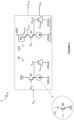
- FIG. 1 is a schematic diagram of previously-considered PPF circuitry 1.
- PPF circuitry 1 comprises a pair of RC filter circuits and an input node configured to receive an input (voltage) signal V IN having a dominant frequency (or peak frequency or tone frequency) f PPF .
- the input signal V IN may for example be a sinusoidal signal.
- Both of the RC filter circuits are source-follower (SF) circuits as indicated.
- the left-hand SF circuit is configured as a low-pass filter and the right-hand SF circuit is configured as a high-pass filter circuit.
- the left-hand SF circuit comprises a field-effect transistor M1 with its gate terminal connected to the input node, with its drain terminal connected to a first supply voltage node (here, VDD or AVD) and with its source terminal connected to a second supply voltage node (here, VSS or AVS, effectively GND or ground) via a current source.
- the voltages at the first and second supply voltage nodes may be considered high and low voltages, or first and second different voltages, respectively.
- the transistor M1 is an N-channel MOSFET (Metal-Oxide-Semiconductor Field-Effect Transistor).
- the source terminal of the field-effect transistor M1 is also connected to the second supply voltage node via a resistor R PPF and a capacitor C PPF connected in series in that order.
- the right-hand SF circuit is configured in the same way as the left-hand SF circuit except that its resistor R PPF and capacitor C PPF are connected in series in the opposite order so as to enable a high-pass function rather than a low-pass function.
- the SF arrangement supplies isolation between the PPF circuitry 1 and a driver circuit (not shown - providing the input signal V IN ), for example a tuned LC-buffer, to avoid resistive/capacitive loading by the PPF circuitry 1 on the driver circuit. That is, the SF arrangement acts as a buffer to minimize or reduce loading on preceding stages.
- the left-hand SF circuit is configured as an RC low-pass filter circuit with pole cut-off frequency equal to the frequency of operation f PPF to create a 45° lagging (voltage) signal V LAG at a node between the resistor R PPF and capacitor C PPF as indicated, with 0.707 ( ⁇ 2) attenuation.
- the right-hand SF circuit is configured as an RC high-pass filter circuit with a zero at the origin and a pole at the frequency of operation f PPF to create a 45° leading (voltage) signal V LEAD at a node between the capacitor C PPF and resistor R PPF as indicated, also with 0.707 ( ⁇ 2) attenuation.
- the nodes at which the signals V LAG and V LEAD are generated may be considered output nodes of the PPF circuitry 1, and those signals may similarly be referred to as output signals of the PPF circuitry 1.
- Figure 2 is a schematic diagram of an equivalent circuit 2 of the PPF circuitry 1.
- Equivalent circuit 2 comprise a pair of equivalent circuits or sub-circuits, one for each of the SF circuits of Figure 1 as indicated.
- the left-hand equivalent circuit represents the low-pass filter and the right-hand equivalent circuit represents the high-pass filter.
- the SF has an equivalent output resistance of 1/g m,M1 , where g m,M1 is the transconductance of the transistor M1, which appears as a series resistance at the input node where the input signal V IN is received.
- This equivalent output resistance 1/g m,M1 may be referred to as the output resistance R M1 seen at the source terminal of the transistor M 1.
- This resistance R M1 is therefore shown in series with the resistor R PPF and capacitor C PPF in line with the left-hand SF circuit of Figure 1 .
- the resistance R M1 has the effect of shifting the filter pole.
- 1/g m,M1 typically needs to be at least ten times smaller than the resistance of R PPF , or the presence of the resistance R M1 needs to be designed into the value of R PPF .
- the transconductance g m,M1 cannot be increased arbitrarily without loading the driver stage, which places a lower-limit on the resistance of R PPF . Consequently, the capacitance of the capacitor C PPF has an upper limit to keep the same pole location.
- the PPF circuitry 1 has been found to suffer from large amplitude and/or phase variation across process corners. This variation may in part be due to non-linearities and PVT variations.
- a process corner here may be taken as an example of a "design-of-experiments" technique, known in semiconductor manufacturing, that refers to a variation of fabrication parameters used in applying an integrated circuit design to a semiconductor wafer.
- Process corners represent the extremes of these parameter variations within which a circuit that has been etched onto the wafer must function correctly.
- a circuit employing devices fabricated at these process corners may run slower or faster than specified and at lower or higher temperatures and voltages, or may not function at all (and be considered to have inadequate design margin).
- NMOS N-channel MOSFET
- PMOS P channel
- Fast and slow corners exhibit carrier mobilities that are higher and lower than normal, respectively.
- a corner designated as fs denotes fast N-channel MOSFETs and slow P-channel MOSFETs.
- Corners may also be defined in terms of temperature: low (l) and high (h).
- the main reason for the large spread in amplitude and/or phase across process corners is the pole frequency location which depends heavily on the resistor R PPF and capacitor C PPF process corners, which are normally uncorrelated.
- the low value of the capacitance of the capacitor C PPF in the PPF circuit 1 as mentioned earlier also makes the PPF circuit 1 sensitive to loading capacitance of the succeeding stage, resulting in more spread across corners.
- the arrangements disclosed herein seek to address such problems by configuring the PPF circuitry, and its constituent filter circuits, to reduce the number of different types of device (transistors, capacitors, resistors) required, as will become apparent.
- both the capacitors and resistors are implemented using the same device type, which results in tracking across process deviation and much lower process deviation spread in comparison with the PPF circuitry 1.
- the arrangements disclosed herein significantly reduce the effect of process corner variation on PPF performance.
- FIG. 3 is a schematic diagram of PPF circuitry 10 embodying the present invention.
- PPF circuitry 10 comprises a pair of RC filter circuits (or circuits which may have RC filter circuits as equivalent circuits), shown in separate dashed boxes, and an input node configured to receive an input signal V IN having a dominant frequency (or peak frequency or tone frequency) f PPF .
- RC filter will be used herein for ease of explanation, understanding that the disclosed circuits function as RC filter circuits (in the sense of an RC circuit configured with discrete R and C components being an equivalent circuit), even when the R component of the RC filter function is not implemented by a discrete/passive resistor as such. The present disclosure will be understood accordingly.
- One of the RC filter circuits is a source-follower (SF) circuit, as indicated, and the other of the RC filter circuits is a source-degenerated common-source amplifier (CSA) circuit, also as indicated.
- the left-hand SF circuit is configured as (or to act as) a low-pass filter and the right-hand CSA circuit is configured as (or to act as) a low-pass filter and/or a high-pass filter depending on where the output signal is taken from.
- the source-degenerated common-source amplifier circuit will be referred to herein as a common-source amplifier (CSA) circuit for simplicity.
- the left-hand SF circuit is similar to the left-hand SF circuit in Figure 1 , except that the resistor R PPF has been omitted (the resistance of the RC filter function coming from the output resistance as seen at the source terminal of the transistor M1).
- the left-hand SF circuit in Figure 3 comprises a field-effect transistor M1 with its gate terminal connected to the input node, with its drain terminal connected to a first supply voltage node (here, VDD or AVD as before) and with its source terminal connected to a second supply voltage node (here, VSS or AVS as before) via a current source.
- the current source may be replaced with a resistor.
- the source terminal of the field-effect transistor M1 is also connected (directly, i.e.
- a (small) resistor may be connected in series with the capacitor C PPF as long as its effect on pole location is negligible for a given application.
- the right-hand CSA circuit is configured in the same way as the left-hand SF circuit except that the drain terminal of the transistor M1 is connected to the first supply voltage node via a resistor R DRAIN , thus forming the CSA arrangement.
- the drain terminal of the transistor M1 is connected to the first supply voltage node substantially directly via the resistor R DRAIN .
- the SF and CSA arrangements supply isolation between the PPF circuitry 10 and a driver circuit (not shown), i.e. minimizing or reducing loading on preceding stages.
- the left-hand SF circuit is configured as an RC low-pass filter with pole cut-off frequency equal to the frequency of operation f PPF to create a 45° lagging signal V LAG at the source terminal of the transistor M1 as indicated, with 0.707 ( ⁇ 2) attenuation.
- the right-hand CSA circuit is configured to provide an RC high-pass filter function with a zero at the origin and a pole at the frequency of operation f PPF to create a 45° leading signal V LEAD at the drain terminal of the transistor M1 also as indicated, also with 0.707 ( ⁇ 2) attenuation.
- the left-hand SF circuit employs the source-follower output resistance R M1 to create the low-pass filter function along with the capacitor C PPF .
- C PPF represents the capacitance of the capacitor C PPF
- R DRAIN will be used to represent the resistance of the resistor R DRAIN .
- the right-hand CSA circuit employs source degeneration to create a zero at DC (or very low frequency) and a pole at g m,M1 /(2* ⁇ *C PPF ).
- the C PPF value can be much higher.
- the V LAG signal is also available at the source terminal of the transistor M1 of the right-hand CSA circuit, based on a low-pass filter function to that node.
- the V LEAD and V LAG signals may both be taken from the right-hand CSA circuit, and the left-hand SF circuit may then be omitted. If there is significant capacitive loading at the drain terminal of the transistor M1, it may be that only the V LEAD signal is used and the V LAG signal is unused (and hence it is shown in parentheses).
- the V LAG and V LEAD signals from the left-hand SF circuit and right-hand CSA circuit of the PPF circuit 10, respectively, may form output signals of the PFF circuit 10 at corresponding output nodes.
- the V LAG and V LEAD signals from the right-hand CSA circuit of the PPF circuit 10 may form output signals of the PFF circuit 10 (and the left-hand SF circuit may be omitted).
- FIG. 4 is a schematic diagram of PPF circuitry 20 embodying the present invention, which may be considered a development of the PPF circuitry 10.
- PPF circuitry 20 like the PPF circuitry 10, comprises a pair of RC filter circuits (here not shown in separate dashed boxes), one of which is a source-follower (SF) circuit as indicated and the other of which is a source-degenerated common-source amplifier (CSA) circuit as indicated, and an input node configured to receive the input signal V IN having a dominant frequency (or peak frequency or tone frequency) f PPF .
- RC filter circuits in terms of their function, as here the R element of the RC filter is not implemented by a discrete/passive resistance.
- the circuits could be referred to simply as filter circuits, for example.
- the left-hand SF circuit and the right-hand CSA circuit of Figure 4 are the same as the left-hand SF circuit and the right-hand CSA circuit of Figure 3 , respectively, except that the capacitors C PPF are implemented as MOS capacitors, in this example as field-effect transistors configured as MOS capacitors.
- the PPF circuitry 20 exploits the fact that the poles for the left-hand SF circuit and the right-hand CSA circuit are defined by the output resistance 1/g m,M1 , or R M1 , as mentioned earlier.
- each capacitor C PPF is implemented as an NMOS field-effect transistor configured as MOS capacitor.
- the transconductance of M1, i.e. g m,M1 is higher, resulting into lower output resistance R M1 and higher C PPF active capacitance, and vice versa for slow process corners. Consequently, the pole frequency spread across process corners is reduced.
- the resistor R DRAIN is also implemented as a field-effect transistor, in this case as a diode-connected NMOS field-effect transistor M2.
- the diode-connected transistor M2 is connected in series (i.e. with its channel in series) between the drain terminal of the transistor M1 of the right-hand CSA circuit and the first supply voltage node (here, VDD), substantially directly.
- the current sources may also be implemented as a field-effect transistor, in this case as an NMOS field-effect transistor M3 whose gate voltage is controlled by a reference voltage V REF to control the drain current I D .
- V REF a reference voltage
- the variation 20X is one example implementation of a current source using a field-effect transistor; other example implementations (not shown) may be employed such as a field-effect transistor in series with a resistor (which resistor could be implemented as a field-effect transistor, such as a diode-connected field-effect transistor).
- the current sources may be replaced with resistors, which again could each be implemented as a field-effect transistor, such as a diode-connected field-effect transistor. The present disclosure will be understood accordingly.
- the gain of the signal V LEAD in the right-hand CSA circuit is g m,M1 /g m,M2 , where g m,M2 is the transconductance of the transistor M2, which has low spread across corners if the M1 and M2 devices are of the same or similar type and/or of the same semiconductor fabrication process and/or have the same or similar fabrication parameters.
- g m,M2 is the transconductance of the transistor M2
- devices M1 and M2 are of the same fabrication process, their fabrication parameters and masks may be the same as in mass production of a product.
- all fabrication processes have uncontrollable variations, which lead to circuit variation on different chips but much less variation of transistors/devices in close proximity.
- FIG. 5 is a schematic diagram of PPF circuitry 30 embodying the present invention, which may be considered a development of the PPF circuitry 20.
- PPF circuitry 30 like the PPF circuitry 10 and 20, comprises a pair of "RC filter” circuits (again, not shown in separate dashed boxes), one of which is a source-follower (SF) circuit as indicated and the other of which is a source-degenerated common-source amplifier (CSA) circuit as indicated, and an input node configured to receive the input signal V IN having a dominant frequency f PPF .
- RC filter a source-follower
- CSA common-source amplifier
- the left-hand SF circuit and the right-hand CSA circuit of Figure 5 are the same as the left-hand SF circuit and the right-hand CSA circuit of Figure 4 , respectively, except that the capacitors C PPF are each implemented as a pair of MOS capacitors, C PPF1 and C PPF2 .
- the capacitors C PPF1 and C PPF2 are implemented as field-effect transistors, here NMOS transistors, configured as MOS capacitors.
- C PPF1 is connected between the source terminal of the transistor M1 and the first supply voltage node (here, VDD), substantially directly
- C PPF2 is connected between the source terminal of the transistor M1 and the second supply voltage node (here, VSS), again substantially directly.
- the capacitors C PPF1 and C PPF2 may have substantially the same capacitance as one another, effectively dividing the capacitor C PPF into two halves. By dividing the capacitor C PPF into two halves, one connected to the first supply voltage node and the other connected to the second supply voltage node, performance is further improved. Using this technique, the C PPF MOS capacitor variation in capacitor versus the voltage swing which would be experienced in Figure 4 is reduced in Figure 5 .
- V LAG increases, the C PPF1 capacitance decreases, whereas the C PPF2 capacitance increases, and vice versa for V LAG decrease.
- PPFs may output a plurality of output signals having different relative phases (e.g. V LAG , V LEAD ) based on an input signal (e.g. V IN ).
- Figures 6 and 7 present schematic views of PPF circuitry 40A, 40B, 40C, and 40D to give examples of such different arrangements of PPF circuitry.
- PPF circuitry 40A may be understood to generate output signals V LAG and V LEAD based on the input signal V IN , and to comprise a SF circuit and a CSA circuit. PPF circuitry 40A may therefore be the same as any of PFF circuitry 10, 20 and 30, where the output signal V LAG is, or is derived from, the signal V LAG of the left-hand SF circuit, and where the output signal V LEAD is, or is derived from, the signal V LEAD of the right-hand CSA circuit.
- PPF circuitry 40B may be understood to generate output signals V LAG and V LEAD based on the input signal V IN , and to comprise two CSA circuits. Each CSA circuit of the PPF circuitry 40B may therefore be the same as the CSA circuit of any of PFF circuitry 10, 20 and 30. That is, the CSA circuits of the PPF circuitry 40B may both be the same as the CSA circuit of the same PPF circuitry of PFF circuitry 10, 20 and 30, or may be the same as the CSA circuits from respective different PPF circuitry of PFF circuitry 10, 20 and 30.
- the output signal V LAG is, or is derived from, the signal V LAG of the left-hand CSA circuit
- the output signal V LEAD is, or is derived from, the signal V LEAD of the right-hand CSA circuit.
- PPF circuitry 40C may be understood to generate output signals V LAG and V LEAD based on the input signal V IN , and to comprise (only) one CSA circuit.
- the CSA circuit of the PPF circuitry 40C may be the same as the CSA circuit of any of PFF circuitry 10, 20 and 30.
- the output signals V LAG and V LEAD are, or are derived from, the signals V LAG and V LEAD of the same CSA circuit. As mentioned earlier, this arrangement may be suitable where there is negligible capacitive loading.
- PPF circuitry 40D may be understood to generate output signals V LAG1 and V LAG2 (which may be compared to output signals V LAG and V LEAD in that they have different relative phases) based on the input signal V IN , and to comprise two SF circuits.
- Each SF circuit of the PPF circuitry 40D may therefore be the same as the SF circuit of any of PFF circuitry 10, 20 and 30. That is, the SF circuits of the PPF circuitry 40D may both be the same as the SF circuit of the same PPF circuitry of PFF circuitry 10, 20 and 30, or may be the same as the SF circuits from respective different PPF circuitry of PFF circuitry 10, 20 and 30.
- the output signal V LAG1 is, or is derived from, the signal V LAG of the left-hand SF circuit
- the output signal V LAG2 is, or is derived from, the signal V LAG of the right-hand SF circuit.
- the resistance R M1 and/or capacitance C PPF may be configured differently between the two SF circuits as would be understood by the skilled person. References to circuits generating output signals V LAG and V LEAD may therefore be considered to also apply to circuits generating output signals V LAG1 and V LAG2 , where PPF circuitry 40D is involved, and the present disclosure will be understood accordingly.
- the PFF circuitry considered above focuses on outputting a plurality of output signals having different relative phases (e.g. V LAG , V LEAD ) based on a single input signal (e.g. V IN ).
- V LAG , V LEAD may have relative phases 0° and 90° and be referred to as I and Q phases, respectively.
- Multiple sets of such PPF circuitry could however be provided to operate based on different such input signals.
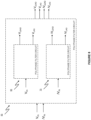
- FIG 8 is a schematic diagram of PPF circuitry 50 embodying the present invention.
- PPF circuitry 50 comprises two sets of PPF circuitry 60 and 70.
- the PPF circuitry 60 may be taken to be the same as any of the PPF circuitry 10, 20, 30, 40A, 40B, 40C, 40D described above, and thus comprises an input node configured to receive the input signal V IN and to output output signals V LAG and V LEAD .
- the PPF circuitry 70 may also be taken to be the same as any of the PPF circuitry 10, 20, 30, 40A, 40B, 40C, 40D described above, except that it is connected to receive an input signal /V IN rather than the input signal V IN , wherein V IN and /V IN are complementary signals.
- the PPF circuitry 70 therefore outputs signals /V LAG and /V LEAD instead of signals V LAG and V LEAD , respectively, where signals /V LAG and /V LEAD may be considered complementary signals of signals V LAG and V LEAD , respectively.
- the PPF circuitry 50 may be considered to have first and second input nodes for receiving input signals V IN and /V IN , respectively, and to output output signals V LAG , V LEAD , /V LAG and /V LEAD .
- V IN and /V IN are complementary signals (i.e.
- the output signals V LAG , V LEAD , /V LAG and /V LEAD may constitute a set of quadrature output signals, which may have relative phases 0°, 90°, 180° and 270°, respectively, and which may be referred to as I+, Q+, I- and Q- phases, respectively.
- the PPF circuitry 50 may be, or be part of, quadrature oscillator circuitry.
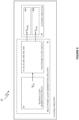
- FIG. 9 is a schematic diagram of clocked circuitry 80 embodying the present invention, comprising multi-phase clock generation circuitry 82 also embodying the present invention.
- Clock signals herein may be considered oscillator signals.
- the multi-phase clock generation circuitry 82 may be considered to comprise any of the PPF circuitry 10, 20, 30, 40A, 40B, 40C, 40D described above, and a source clock generation circuit 84 configured to generate and provide to the polyphase filter circuitry the input signal V IN as a source clock signal.
- the output signals of the polyphase filter circuitry are then the output clock signals of the multi-phase clock generation circuitry 82 and have different relative phases from one another.
- the clocked circuitry 80 comprises the multi-phase clock generation circuitry 82 and one or more clocked circuits 86 connected to receive the output clock signals of the polyphase filter circuitry and to operate based thereon.
- clocked circuits 86A and 86B operating based on the output signals V LAG and V LEAD , respectively, are shown.
- one or more clocked circuits 86 may be connected to receive the output clock signals.
- Figure 10 is a schematic diagram of clocked circuitry 90 embodying the present invention, comprising multi-phase clock generation circuitry 92 also embodying the present invention.
- the multi-phase clock generation circuitry 92 may be considered to comprise the PPF circuitry 50 described above, and a source clock generation circuit 94 configured to generate and provide to the polyphase filter circuitry the input signals V IN and /V IN as source clock signals.
- the output signals of the polyphase filter circuitry 50 are then the output clock signals of the multi-phase clock generation circuitry 92 and have different relative phases from one another.
- the clocked circuitry 90 comprises the multi-phase clock generation circuitry 92 and one or more clocked circuits 96 connected to receive the output clock signals of the polyphase filter circuitry 50 and to operate based thereon.
- the clocked circuitry 80 or 90, or the multi-phase clock generation circuitry 82 or 92 may be or be part of quadrature oscillator circuitry, phase lock loop circuitry (PLL), an analogue-to-digital converter (ADC), a digital-to-analogue converter (DAC), Serializer/Deserializer circuits (SERDES), Clock Data Recovery circuits (CDRs), Wireless Transceivers, Processors, IQ phase generation circuitry or clocking circuitry.
- PLL phase lock loop circuitry
- ADC analogue-to-digital converter
- DAC digital-to-analogue converter
- SERDES Serializer/Deserializer circuits
- CDRs Clock Data Recovery circuits
- Wireless Transceivers Wireless Transceivers, Processors, IQ phase generation circuitry or clocking circuitry.
- Figure 11 presents a graphical output of simulation results based on a simulation of the multi-phase clock generation circuitry 92 (see Figure 10 ), where the PPF circuitry 60 and the PPF circuitry 70 of the PPF circuitry 50 (see Figure 8 ) are each the same as the PPF circuitry 30 (see Figure 5 ). Also, for each instance of the PPF circuitry 30, the output signal V LEAD (or /V LEAD ) is generated by the CSA circuit and the output signal V LAG (or /V LAG ) is generated by the SF circuit.
- the graph shows the simulation of the output signals V LAG , V LEAD , /V LAG and /V LEAD across process corners (see the lefthand panel), in this case (for the transistors) typical-typical (tt), slow-slow (ss), and fast-fast (ff), as mentioned earlier.
- Temperature corners are also taken into account, giving traces for V LEAD in the order as in the left-hand panel for tt room temperature (tt*t), ss high temperature (ss*h), ss low temperature (ss*l), ff high temperature (ff*h) and ff low temperature (ff*l), where tt*t corresponds to trace ttttttt whose label starts with tt and ends with t (the intermediate letters being ignored for these purposes).
- These traces for V LEAD are labelled a to e, respectively, and are those whose peaks align with the label V LEAD above the graph.
- Corresponding traces are also provided for V LAG , /V LEAD and /V LAG but are not listed specifically in the lefthand panel.
- the labels M1, M2, M3 and M4 in Figure 11 are markers marking four readings to indicate the spread, and do not correspond to the reference signs M1 and M2 for transistors in the earlier Figures.
- the spread across process and temperature is relatively low, and is lower for V LAG and /V LAG than for V LEAD and /V LEAD .
- the resistance R DRAIN (see Figure 5 ) affects the gain of V LEAD and /V LEAD and the signals V LAG and /V LAG do not have this additional factor.
- the reason for the spread is the extra parasitic capacitance at the V LEAD node which creates an extra parasitic pole that can slightly shift the V LEAD signal. The extra pole is not present for the V LAG signal.
- the multi-phase clock generation circuitry 92 exhibits minimal spread across process and temperature.
- the circuitry disclosed herein enables implementation of PPF with reduced phase/amplitude spread across process corners to improve overall system performance. It will also be appreciated that the component RC filter circuits of the PPF circuitry disclosed herein contribute to the PPF performance. Accordingly, the present invention extends to the SF or CSA circuits individually (or combinations thereof) of PPF circuitry 10, 20 and 30.
- a source-follower circuit comprising: an input node configured to receive the input signal V IN having a dominant frequency f PPF ; a field-effect transistor M1 with its gate terminal connected to the input node; and a capacitor C PPF connected to the source terminal of the field-effect transistor M1, wherein: the output resistance R M1 seen at the source terminal of the field-effect transistor M1 and the capacitance of the capacitor C PPF are configured to define the frequency response of the source-follower circuit so that, based on the input signal V IN , a signal V LAG is generated at the source terminal of the transistor M1 which lags the input signal VIN in phase by a given phase shift ⁇ LAG .
- the capacitor C PFF may be substantially directly connected between the source terminal of the field-effect transistor and a supply voltage node and be implemented as a MOS capacitor (e.g. as a field-effect transistor configured as the MOS capacitor).
- the capacitor C PFF may be implemented as a capacitor C PPF1 and a capacitor C PPF2 as described earlier.
- a common-source amplifier circuit comprising: the source-follower circuit, and a resistor R DRAIN (which may be a diode-connected field-effect transistor) connected between the drain terminal of the transistor and a supply voltage node.
- a signal V LEAD may be generated at the drain terminal of the transistor M1 which leads the input signal V IN in phase by a given phase shift ⁇ LEAD .
- the field-effect transistors may be of the same or similar type and/or of the same semiconductor fabrication process.
- FIG. 12 is a schematic diagram of integrated circuitry 100 embodying the present invention.
- the integrated circuitry 100 may comprise any of the PPF circuitry (such as PPF circuitry 10, 20, 30, 40A, 40B, 40C, 40D, 50), indicated as PPF circuitry 30 in Figure 12 for simplicity, the SF or CSA circuits thereof (indicated as 30(SF), 30(CSA) in Figure 12 for simplicity, or the multi-phase clock generation circuitry 82 or 92, or the clocked circuitry 80 or 90.
- PPF circuitry such as PPF circuitry 10, 20, 30, 40A, 40B, 40C, 40D, 50
- the SF or CSA circuits thereof indicated as 30(SF), 30(CSA) in Figure 12 for simplicity
- the multi-phase clock generation circuitry 82 or 92 or the clocked circuitry 80 or 90.
- Integrated circuitry 100 may be representative of some or all of an IC chip.
- the present invention extends to integrated circuitry and IC chips as mentioned above, circuit boards comprising such IC chips, and communication networks (for example, internet fiber-optic networks and wireless networks) and network equipment of such networks, comprising such circuit boards.
- communication networks for example, internet fiber-optic networks and wireless networks
Landscapes
- Engineering & Computer Science (AREA)
- Power Engineering (AREA)
- Physics & Mathematics (AREA)
- Computer Hardware Design (AREA)
- Mathematical Physics (AREA)
- Networks Using Active Elements (AREA)
Abstract
Polyphase filter circuitry, comprising: an input node configured to receive an input signal VIN having a dominant frequency fPPF; and a common-source amplifier circuit, wherein: the common-source amplifier circuit comprises a field-effect transistor M1 with its gate terminal connected to the input node and with a capacitor CPFF connected to its source terminal; and for the common-source amplifier circuit, the output resistance RM1 seen at the source terminal of the field-effect transistor M1 and the capacitance of the capacitor CPFF are configured to define the frequency response of the common-source amplifier circuit so that, based on the input signal VIN, a signal VLEAD is generated at the drain terminal of the transistor M1 which leads the input signal VIN in phase by a given phase shift ΔφLEAD and a signal VLAG is generated at the source terminal of the transistor M1 which lags the input signal VIN in phase by a given phase shift ΔφLAG.
Description
- The present invention relates to filter circuitry, including circuitry thereof, and circuitry comprising the same. Such filter circuitry may comprise source-follower and/or common-source amplifier circuitry.
- More specifically, the present disclosure relates to polyphase filter (Poly-Phase Filter, or PPF) circuitry, as an example filter type. PPF circuitry may be used to generate multiple output signals which have different relative phases based on one or more input signals. Such signals may be clock signals.
- For example, as a running example, PPF circuitry may be used to generate a pair of clock signals (VLEAD, VLAG) which are 90° out of phase with one another (e.g. I and Q clock signals) based on an input clock signal VIN. As another running example, PPF circuitry may be used to generate quadrature clock signals (VLEAD, VLAG, /VLEAD, /VLAG) which have relative phases 0°, 90°, 180° and 270°, respectively, and which may be referred to as I+, Q+, I- and Q- phases, respectively.
- PPF circuitry may be used in clocked circuitry in general, for example in quadrature oscillator circuitry, phase lock loop circuitry (PLL), an analogue-to-digital converter (ADC), a digital-to-analogue converter (DAC), Serializer/Deserializer circuits (SERDES), Clock Data Recovery circuits (CDRs), Wireless Transceivers, Processors, IQ phase generation circuitry or clocking circuitry.
- It has been found that the performance of previously-considered such circuitry is subject to considerable distortion, which is particularly exacerbated at high frequencies.
- It is desirable to address such problems.
- According to an embodiment of a first aspect of the present invention, there is provided polyphase filter circuitry, comprising: an input node configured to receive an input signal VIN having a dominant frequency fPPF; and a common-source amplifier circuit, wherein: the common-source amplifier circuit comprises a field-effect transistor M1 with its gate terminal connected to the input node and with a capacitor CPFF connected to its source terminal; and for the common-source amplifier circuit, the output resistance RM1 seen at the source terminal of the field-effect transistor M1 and the capacitance of the capacitor CPFF are configured to define the frequency response of the common-source amplifier circuit so that, based on the input signal VIN, a signal VLEAD is generated at the drain terminal of the transistor M1 which leads the input signal VIN in phase by a given phase shift ΔφLEAD and a signal VLAG is generated at the source terminal of the transistor M1 which lags the input signal VIN in phase by a given phase shift ΔφLAG.
- The signals VLEAD and VLAG of the common-source amplifier circuit may be output signals of the polyphase filter circuitry.
- The polyphase filter circuitry may comprise first and second said common-source amplifier circuits, wherein the signal VLEAD of the first common-source amplifier circuit and the signal VLAG of the second common-source amplifier circuit are output signals of the polyphase filter circuitry.
- The polyphase filter circuitry may further comprise a source-follower circuit, wherein: the source-follower circuit comprises a field-effect transistor M1 with its gate terminal connected to the input node and with a capacitor CPPF connected to its source terminal; and for the source-follower circuit, the output resistance RM1 seen at the source terminal of the field-effect transistor M1 and the capacitance of the capacitor CPPF are configured to define the frequency response of the source-follower circuit so that, based on the input signal VIN, a signal VLAG is generated at the source terminal of the transistor M1 which lags the input signal VIN in phase by a given phase shift ΔφLAG.
- According to an embodiment of a second aspect of the present invention, there is provided polyphase filter circuitry, comprising: an input node configured to receive an input signal VIN having a dominant frequency fPPF; and first and second source-follower circuits, wherein: each source-follower circuit comprises a field-effect transistor M1 with its gate terminal connected to the input node and with a capacitor CPPF connected to its source terminal; for each source-follower circuit, the output resistance RM1 seen at the source terminal of the field-effect transistor M1 and the capacitance of the capacitor CPPF are configured to define the frequency response of the source-follower circuit so that, based on the input signal VIN, a signal VLAG is generated at the source terminal of the transistor M1 which lags the input signal VIN in phase by a given phase shift ΔφLAG; the given phase shifts ΔφLAG for the first and second source-follower circuits are different from one another; and the signals VLAG of the first and second source-follower circuits are output signals of the polyphase filter circuitry.
- According to an embodiment of a third aspect of the present invention, there is provided multi-phase clock generation circuitry comprising: the polyphase filter circuitry of the aforementioned first or second aspect; and a source clock generation circuit configured to generate and provide to the polyphase filter circuitry the input signal VIN as a source clock signal (or input signals VIN and /VIN as source clock signals - see the arrangements disclosed later herein), the output signals of the polyphase filter circuitry being output clock signals of the multi-phase clock generation circuitry having different relative phases from one another.
- According to an embodiment of a fourth aspect of the present invention, there is provided clocked circuitry, comprising: the multi-phase clock generation circuitry of the aforementioned third aspect; and one or more clocked circuits connected to receive the output clock signals and operate based thereon.
- According to an embodiment of a fifth aspect of the present invention, there is provided a source-follower circuit, comprising: an input node configured to receive an input signal VIN having a dominant frequency fPPF; a field-effect transistor M1 with its gate terminal connected to the input node; and a capacitor CPPF connected to the source terminal of the field-effect transistor M1, wherein: the output resistance RM1 seen at the source terminal of the field-effect transistor M1 and the capacitance of the capacitor CPPF are configured to define the frequency response of the source-follower circuit so that, based on the input signal VIN, a signal VLAG is generated at the source terminal of the transistor M1 which lags the input signal VIN in phase by a given phase shift ΔφLAG; the capacitor CPFF is substantially directly connected between the source terminal of the field-effect transistor and a supply voltage node and is implemented as a MOS capacitor.
- According to an embodiment of a sixth aspect of the present invention, there is provided a common-source amplifier circuit, comprising: the source-follower circuit of the aforementioned fifth aspect; and a resistor RDRAIN connected between the drain terminal of the transistor and a supply voltage node, optionally wherein a signal VLEAD is generated at the drain terminal of the transistor M1 which leads the input signal VIN in phase by a given phase shift ΔφLEAD.
- According to an embodiment of a seventh aspect of the present invention, there is provided a source-follower circuit, comprising: an input node configured to receive an input signal VIN; a field-effect transistor M1 with its gate terminal connected to the input node; and a capacitor CPPF connected to the source terminal of the field-effect transistor M1, wherein: the capacitor CPFF is substantially directly connected between the source terminal of the field-effect transistor and a supply voltage node and is implemented as a MOS capacitor.
- According to an embodiment of an eighth aspect of the present invention, there is provided a common-source amplifier circuit, comprising: the source-follower circuit of the aforementioned seventh aspect; and a resistor RDRAIN connected between the drain terminal of the transistor and a supply voltage node.
- According to an embodiment of a ninth aspect of the present invention, there is provided integrated circuitry, such as an IC chip, comprising the polyphase filter circuitry of the aforementioned first or second aspect, or the multi-phase clock generation circuitry of the aforementioned third aspect, or the clocked circuitry of the aforementioned fourth aspect, or the source-follower circuit or common-source amplifier circuit of any of the aforementioned fifth to eighth aspects.
- Also envisaged are corresponding method aspects. Preferred features of one aspect may be applied to another aspect, and vice versa.
- Reference will now be made, by way of example, to the accompanying drawings, of which:
-
Figure 1 is a schematic diagram of previously-considered PPF circuitry; -
Figure 2 is a schematic diagram of an equivalent circuit of the PPF circuitry ofFigure 1 ; -
Figures 3 to 8 present schematic diagrams of PPF circuitry embodying the present invention; -
Figures 9 and10 are each schematic diagrams of clocked circuitry and multi-phase clock generation circuitry embodying the present invention; -
Figure 11 presents a graphical output of simulation results based on a simulation of multi-phase clock generation circuitry; and -
Figure 12 is a schematic diagram of integrated circuitry embodying the present invention. - In order to better appreciate problems with previously-considered filter circuitry, reference will be made to
Figures 1 and2 . -
Figure 1 is a schematic diagram of previously-consideredPPF circuitry 1.PPF circuitry 1 comprises a pair of RC filter circuits and an input node configured to receive an input (voltage) signal VIN having a dominant frequency (or peak frequency or tone frequency) fPPF. The input signal VIN may for example be a sinusoidal signal. - Both of the RC filter circuits are source-follower (SF) circuits as indicated. The left-hand SF circuit is configured as a low-pass filter and the right-hand SF circuit is configured as a high-pass filter circuit.
- In detail, the left-hand SF circuit comprises a field-effect transistor M1 with its gate terminal connected to the input node, with its drain terminal connected to a first supply voltage node (here, VDD or AVD) and with its source terminal connected to a second supply voltage node (here, VSS or AVS, effectively GND or ground) via a current source. The voltages at the first and second supply voltage nodes may be considered high and low voltages, or first and second different voltages, respectively. The transistor M1 is an N-channel MOSFET (Metal-Oxide-Semiconductor Field-Effect Transistor). The source terminal of the field-effect transistor M1 is also connected to the second supply voltage node via a resistor RPPF and a capacitor CPPF connected in series in that order.
- The right-hand SF circuit is configured in the same way as the left-hand SF circuit except that its resistor RPPF and capacitor CPPF are connected in series in the opposite order so as to enable a high-pass function rather than a low-pass function.
- The SF arrangement supplies isolation between the
PPF circuitry 1 and a driver circuit (not shown - providing the input signal VIN), for example a tuned LC-buffer, to avoid resistive/capacitive loading by thePPF circuitry 1 on the driver circuit. That is, the SF arrangement acts as a buffer to minimize or reduce loading on preceding stages. - As a running example, it will be assumed that the left-hand SF circuit is configured as an RC low-pass filter circuit with pole cut-off frequency equal to the frequency of operation fPPF to create a 45° lagging (voltage) signal VLAG at a node between the resistor RPPF and capacitor CPPF as indicated, with 0.707 (√2) attenuation. Similarly, it will be assumed that the right-hand SF circuit is configured as an RC high-pass filter circuit with a zero at the origin and a pole at the frequency of operation fPPF to create a 45° leading (voltage) signal VLEAD at a node between the capacitor CPPF and resistor RPPF as indicated, also with 0.707 (√2) attenuation.
- The nodes at which the signals VLAG and VLEAD are generated may be considered output nodes of the
PPF circuitry 1, and those signals may similarly be referred to as output signals of thePPF circuitry 1. -
Figure 2 is a schematic diagram of anequivalent circuit 2 of thePPF circuitry 1. -
Equivalent circuit 2 comprise a pair of equivalent circuits or sub-circuits, one for each of the SF circuits ofFigure 1 as indicated. The left-hand equivalent circuit represents the low-pass filter and the right-hand equivalent circuit represents the high-pass filter. - In detail, looking at the left-hand equivalent circuit (corresponding to the left-hand SF circuit of
Figure 1 ), the SF has an equivalent output resistance of 1/gm,M1, where gm,M1 is the transconductance of the transistor M1, which appears as a series resistance at the input node where the input signal VIN is received. Thisequivalent output resistance 1/gm,M1 may be referred to as the output resistance RM1 seen at the source terminal of thetransistor M 1. This resistance RM1 is therefore shown in series with the resistor RPPF and capacitor CPPF in line with the left-hand SF circuit ofFigure 1 . - The resistance RM1 has the effect of shifting the filter pole. For the resistance RM1 to have a negligible effect on pole location, 1/gm,M1 typically needs to be at least ten times smaller than the resistance of RPPF, or the presence of the resistance RM1 needs to be designed into the value of RPPF. The transconductance gm,M1 cannot be increased arbitrarily without loading the driver stage, which places a lower-limit on the resistance of RPPF. Consequently, the capacitance of the capacitor CPPF has an upper limit to keep the same pole location.
- Similar analysis, taking into
account 1/gm,M1, may be applied to the right-hand equivalent circuit (corresponding to the right-hand SF circuit ofFigure 1 ). - Looking at
Figures 1 and2 , thePPF circuitry 1 has been found to suffer from large amplitude and/or phase variation across process corners. This variation may in part be due to non-linearities and PVT variations. - A process corner here may be taken as an example of a "design-of-experiments" technique, known in semiconductor manufacturing, that refers to a variation of fabrication parameters used in applying an integrated circuit design to a semiconductor wafer. Process corners represent the extremes of these parameter variations within which a circuit that has been etched onto the wafer must function correctly. A circuit employing devices fabricated at these process corners may run slower or faster than specified and at lower or higher temperatures and voltages, or may not function at all (and be considered to have inadequate design margin).
- Taking field-effect transistors as an example, one naming convention for process corners (adopted in
Figure 11 described later herein) is to use two-letter designators, where the first letter refers to the N-channel MOSFET (NMOS) corner, and the second letter refers to the P channel (PMOS) corner. In this naming convention, three corners exist: typical (t), fast (f) and slow (s). Fast and slow corners exhibit carrier mobilities that are higher and lower than normal, respectively. For example, a corner designated as fs denotes fast N-channel MOSFETs and slow P-channel MOSFETs. There are therefore five possible corners: typical-typical (tt), fast-fast (ff), slow-slow (ss), fast-slow (fs), and slow-fast (sf). Corners may also be defined in terms of temperature: low (l) and high (h). - The main reason for the large spread in amplitude and/or phase across process corners is the pole frequency location which depends heavily on the resistor RPPF and capacitor CPPF process corners, which are normally uncorrelated. The low value of the capacitance of the capacitor CPPF in the
PPF circuit 1 as mentioned earlier also makes thePPF circuit 1 sensitive to loading capacitance of the succeeding stage, resulting in more spread across corners. - The arrangements disclosed herein seek to address such problems by configuring the PPF circuitry, and its constituent filter circuits, to reduce the number of different types of device (transistors, capacitors, resistors) required, as will become apparent. In some arrangements, both the capacitors and resistors are implemented using the same device type, which results in tracking across process deviation and much lower process deviation spread in comparison with the
PPF circuitry 1. The arrangements disclosed herein significantly reduce the effect of process corner variation on PPF performance. -
Figure 3 is a schematic diagram ofPPF circuitry 10 embodying the present invention. -
PPF circuitry 10 comprises a pair of RC filter circuits (or circuits which may have RC filter circuits as equivalent circuits), shown in separate dashed boxes, and an input node configured to receive an input signal VIN having a dominant frequency (or peak frequency or tone frequency) fPPF. The terminology "RC filter" will be used herein for ease of explanation, understanding that the disclosed circuits function as RC filter circuits (in the sense of an RC circuit configured with discrete R and C components being an equivalent circuit), even when the R component of the RC filter function is not implemented by a discrete/passive resistor as such. The present disclosure will be understood accordingly. - One of the RC filter circuits is a source-follower (SF) circuit, as indicated, and the other of the RC filter circuits is a source-degenerated common-source amplifier (CSA) circuit, also as indicated. The left-hand SF circuit is configured as (or to act as) a low-pass filter and the right-hand CSA circuit is configured as (or to act as) a low-pass filter and/or a high-pass filter depending on where the output signal is taken from. The source-degenerated common-source amplifier circuit will be referred to herein as a common-source amplifier (CSA) circuit for simplicity.
- The left-hand SF circuit is similar to the left-hand SF circuit in
Figure 1 , except that the resistor RPPF has been omitted (the resistance of the RC filter function coming from the output resistance as seen at the source terminal of the transistor M1). In detail, the left-hand SF circuit inFigure 3 comprises a field-effect transistor M1 with its gate terminal connected to the input node, with its drain terminal connected to a first supply voltage node (here, VDD or AVD as before) and with its source terminal connected to a second supply voltage node (here, VSS or AVS as before) via a current source. In some arrangements the current source may be replaced with a resistor. The source terminal of the field-effect transistor M1 is also connected (directly, i.e. without a series-connected discrete resistor) to the second supply voltage node via a capacitor CPPF. In practice, a (small) resistor may be connected in series with the capacitor CPPF as long as its effect on pole location is negligible for a given application. - The right-hand CSA circuit is configured in the same way as the left-hand SF circuit except that the drain terminal of the transistor M1 is connected to the first supply voltage node via a resistor RDRAIN, thus forming the CSA arrangement. In the arrangement shown, the drain terminal of the transistor M1 is connected to the first supply voltage node substantially directly via the resistor RDRAIN.
- As before, the SF and CSA arrangements supply isolation between the
PPF circuitry 10 and a driver circuit (not shown), i.e. minimizing or reducing loading on preceding stages. - Continuing the running example, it will be assumed that the left-hand SF circuit is configured as an RC low-pass filter with pole cut-off frequency equal to the frequency of operation fPPF to create a 45° lagging signal VLAG at the source terminal of the transistor M1 as indicated, with 0.707 (√2) attenuation. Similarly, it will be assumed that the right-hand CSA circuit is configured to provide an RC high-pass filter function with a zero at the origin and a pole at the frequency of operation fPPF to create a 45° leading signal VLEAD at the drain terminal of the transistor M1 also as indicated, also with 0.707 (√2) attenuation.
- The arrangement of
Figure 3 relaxes the upper limit for CPPF. - To generate the VLAG signal, the left-hand SF circuit employs the source-follower output resistance RM1 to create the low-pass filter function along with the capacitor CPPF. The pole frequency=gm,M1,/(2*π*CPPF) is set to be equal to the operation frequency fPPF. Here, for simplicity, CPPF represents the capacitance of the capacitor CPPF, and similarly RDRAIN will be used to represent the resistance of the resistor RDRAIN.
- To generate the VLEAD signal, the right-hand CSA circuit employs source degeneration to create a zero at DC (or very low frequency) and a pole at gm,M1/(2*π*CPPF).
- As a result, the CPPF value can be much higher.
- As also indicated in
Figure 3 , the VLAG signal is also available at the source terminal of the transistor M1 of the right-hand CSA circuit, based on a low-pass filter function to that node. In situations where there is minimal or negligible capacitive loading at the drain terminal of the transistor M1 of the right-hand CSA circuit, or if the phase requirements are suitable, the VLEAD and VLAG signals may both be taken from the right-hand CSA circuit, and the left-hand SF circuit may then be omitted. If there is significant capacitive loading at the drain terminal of the transistor M1, it may be that only the VLEAD signal is used and the VLAG signal is unused (and hence it is shown in parentheses). - Thus, as indicated in
Figure 3 , the VLAG and VLEAD signals from the left-hand SF circuit and right-hand CSA circuit of thePPF circuit 10, respectively, may form output signals of thePFF circuit 10 at corresponding output nodes. In another arrangement, the VLAG and VLEAD signals from the right-hand CSA circuit of thePPF circuit 10 may form output signals of the PFF circuit 10 (and the left-hand SF circuit may be omitted). -
Figure 4 is a schematic diagram ofPPF circuitry 20 embodying the present invention, which may be considered a development of thePPF circuitry 10. -
PPF circuitry 20, like thePPF circuitry 10, comprises a pair of RC filter circuits (here not shown in separate dashed boxes), one of which is a source-follower (SF) circuit as indicated and the other of which is a source-degenerated common-source amplifier (CSA) circuit as indicated, and an input node configured to receive the input signal VIN having a dominant frequency (or peak frequency or tone frequency) fPPF. It is recalled that these circuits are referred to as "RC filter" circuits in terms of their function, as here the R element of the RC filter is not implemented by a discrete/passive resistance. The circuits could be referred to simply as filter circuits, for example. - The left-hand SF circuit and the right-hand CSA circuit of
Figure 4 are the same as the left-hand SF circuit and the right-hand CSA circuit ofFigure 3 , respectively, except that the capacitors CPPF are implemented as MOS capacitors, in this example as field-effect transistors configured as MOS capacitors. - The
PPF circuitry 20 exploits the fact that the poles for the left-hand SF circuit and the right-hand CSA circuit are defined by theoutput resistance 1/gm,M1, or RM1, as mentioned earlier. In thePPF circuitry 20 each capacitor CPPF is implemented as an NMOS field-effect transistor configured as MOS capacitor. For fast process corners, the transconductance of M1, i.e. gm,M1, is higher, resulting into lower output resistance RM1 and higher CPPF active capacitance, and vice versa for slow process corners. Consequently, the pole frequency spread across process corners is reduced. - In the right-hand CSA circuit (common-source stage), the resistor RDRAIN is also implemented as a field-effect transistor, in this case as a diode-connected NMOS field-effect transistor M2. The diode-connected transistor M2 is connected in series (i.e. with its channel in series) between the drain terminal of the transistor M1 of the right-hand CSA circuit and the first supply voltage node (here, VDD), substantially directly.
- In an
example variation 20X shown in a dashed circle, the current sources may also be implemented as a field-effect transistor, in this case as an NMOS field-effect transistor M3 whose gate voltage is controlled by a reference voltage VREF to control the drain current ID. Although only explicitly shown in respect of the left-hand SF circuit inFigure 4 , this applies equally to all of the current sources of the circuits described herein. Thevariation 20X is one example implementation of a current source using a field-effect transistor; other example implementations (not shown) may be employed such as a field-effect transistor in series with a resistor (which resistor could be implemented as a field-effect transistor, such as a diode-connected field-effect transistor). As another variation (not shown), the current sources may be replaced with resistors, which again could each be implemented as a field-effect transistor, such as a diode-connected field-effect transistor. The present disclosure will be understood accordingly. - In the implementation of
Figure 4 , taking intoaccount variation 20X, all of the discrete components are implemented with field-effect transistors, in this case NMOS field-effect transistors. - The gain of the signal VLEAD in the right-hand CSA circuit (common-source stage) is gm,M1/gm,M2, where gm,M2 is the transconductance of the transistor M2, which has low spread across corners if the M1 and M2 devices are of the same or similar type and/or of the same semiconductor fabrication process and/or have the same or similar fabrication parameters. For example, where devices M1 and M2 are of the same fabrication process, their fabrication parameters and masks may be the same as in mass production of a product. Of course, all fabrication processes have uncontrollable variations, which lead to circuit variation on different chips but much less variation of transistors/devices in close proximity.
-
Figure 5 is a schematic diagram of PPF circuitry 30 embodying the present invention, which may be considered a development of thePPF circuitry 20. - PPF circuitry 30, like the
PPF circuitry - The left-hand SF circuit and the right-hand CSA circuit of
Figure 5 are the same as the left-hand SF circuit and the right-hand CSA circuit ofFigure 4 , respectively, except that the capacitors CPPF are each implemented as a pair of MOS capacitors, CPPF1 and CPPF2. - The capacitors CPPF1 and CPPF2 are implemented as field-effect transistors, here NMOS transistors, configured as MOS capacitors. For each circuit, CPPF1 is connected between the source terminal of the transistor M1 and the first supply voltage node (here, VDD), substantially directly, and CPPF2 is connected between the source terminal of the transistor M1 and the second supply voltage node (here, VSS), again substantially directly.
- The capacitors CPPF1 and CPPF2 may have substantially the same capacitance as one another, effectively dividing the capacitor CPPF into two halves. By dividing the capacitor CPPF into two halves, one connected to the first supply voltage node and the other connected to the second supply voltage node, performance is further improved. Using this technique, the CPPF MOS capacitor variation in capacitor versus the voltage swing which would be experienced in
Figure 4 is reduced inFigure 5 . By way of explanation, as VLAG increases, the CPPF1 capacitance decreases, whereas the CPPF2 capacitance increases, and vice versa for VLAG decrease. - As will be appreciated, various implementations of PPFs are envisaged which may output a plurality of output signals having different relative phases (e.g. VLAG, VLEAD) based on an input signal (e.g. VIN).
Figures 6 and7 present schematic views ofPPF circuitry -
PPF circuitry 40A may be understood to generate output signals VLAG and VLEAD based on the input signal VIN, and to comprise a SF circuit and a CSA circuit.PPF circuitry 40A may therefore be the same as any ofPFF circuitry -
PPF circuitry 40B may be understood to generate output signals VLAG and VLEAD based on the input signal VIN, and to comprise two CSA circuits. Each CSA circuit of thePPF circuitry 40B may therefore be the same as the CSA circuit of any ofPFF circuitry PPF circuitry 40B may both be the same as the CSA circuit of the same PPF circuitry ofPFF circuitry PFF circuitry PPF circuitry 40B, the output signal VLAG is, or is derived from, the signal VLAG of the left-hand CSA circuit, and the output signal VLEAD is, or is derived from, the signal VLEAD of the right-hand CSA circuit. -
PPF circuitry 40C may be understood to generate output signals VLAG and VLEAD based on the input signal VIN, and to comprise (only) one CSA circuit. The CSA circuit of thePPF circuitry 40C may be the same as the CSA circuit of any ofPFF circuitry PPF circuitry 40C, the output signals VLAG and VLEAD are, or are derived from, the signals VLAG and VLEAD of the same CSA circuit. As mentioned earlier, this arrangement may be suitable where there is negligible capacitive loading. -
PPF circuitry 40D may be understood to generate output signals VLAG1 and VLAG2 (which may be compared to output signals VLAG and VLEAD in that they have different relative phases) based on the input signal VIN, and to comprise two SF circuits. Each SF circuit of thePPF circuitry 40D may therefore be the same as the SF circuit of any ofPFF circuitry PPF circuitry 40D may both be the same as the SF circuit of the same PPF circuitry ofPFF circuitry PFF circuitry PPF circuitry 40D, the output signal VLAG1 is, or is derived from, the signal VLAG of the left-hand SF circuit, and the output signal VLAG2 is, or is derived from, the signal VLAG of the right-hand SF circuit. In order to generate output signals VLAG1 and VLAG2 with different relative phases, the resistance RM1 and/or capacitance CPPF (or CPPF1 in combination with CPPF2) may be configured differently between the two SF circuits as would be understood by the skilled person. References to circuits generating output signals VLAG and VLEAD may therefore be considered to also apply to circuits generating output signals VLAG1 and VLAG2, wherePPF circuitry 40D is involved, and the present disclosure will be understood accordingly. - The PFF circuitry considered above focuses on outputting a plurality of output signals having different relative phases (e.g. VLAG, VLEAD) based on a single input signal (e.g. VIN). For example, where the given phase shifts are 45° phase shifts as in the running example, the output signals VLAG, VLEAD may have relative phases 0° and 90° and be referred to as I and Q phases, respectively. Multiple sets of such PPF circuitry could however be provided to operate based on different such input signals.
-
Figure 8 is a schematic diagram ofPPF circuitry 50 embodying the present invention.PPF circuitry 50 comprises two sets ofPPF circuitry - The
PPF circuitry 60 may be taken to be the same as any of thePPF circuitry - The
PPF circuitry 70 may also be taken to be the same as any of thePPF circuitry PPF circuitry 70 therefore outputs signals /VLAG and /VLEAD instead of signals VLAG and VLEAD, respectively, where signals /VLAG and /VLEAD may be considered complementary signals of signals VLAG and VLEAD, respectively. - Overall, therefore, the
PPF circuitry 50 may be considered to have first and second input nodes for receiving input signals VIN and /VIN, respectively, and to output output signals VLAG, VLEAD, /VLAG and /VLEAD. Where VIN and /VIN are complementary signals (i.e. 180° out of phase), and where the phase shifts created in thePPF circuitry 60 andPPF circuitry 70 are all for example 45° as in the running example, the output signals VLAG, VLEAD, /VLAG and /VLEAD may constitute a set of quadrature output signals, which may have relative phases 0°, 90°, 180° and 270°, respectively, and which may be referred to as I+, Q+, I- and Q- phases, respectively. In such a case, thePPF circuitry 50 may be, or be part of, quadrature oscillator circuitry. -
Figure 9 is a schematic diagram of clockedcircuitry 80 embodying the present invention, comprising multi-phaseclock generation circuitry 82 also embodying the present invention. Clock signals herein may be considered oscillator signals. - The multi-phase
clock generation circuitry 82 may be considered to comprise any of thePPF circuitry clock generation circuit 84 configured to generate and provide to the polyphase filter circuitry the input signal VIN as a source clock signal. The output signals of the polyphase filter circuitry are then the output clock signals of the multi-phaseclock generation circuitry 82 and have different relative phases from one another. - The clocked
circuitry 80 comprises the multi-phaseclock generation circuitry 82 and one or more clockedcircuits 86 connected to receive the output clock signals of the polyphase filter circuitry and to operate based thereon. For ease of understanding, individual clockedcircuits circuits 86 may be connected to receive the output clock signals. -
Figure 10 is a schematic diagram of clockedcircuitry 90 embodying the present invention, comprising multi-phaseclock generation circuitry 92 also embodying the present invention. - The multi-phase
clock generation circuitry 92 may be considered to comprise thePPF circuitry 50 described above, and a sourceclock generation circuit 94 configured to generate and provide to the polyphase filter circuitry the input signals VIN and /VIN as source clock signals. The output signals of thepolyphase filter circuitry 50 are then the output clock signals of the multi-phaseclock generation circuitry 92 and have different relative phases from one another. - The clocked
circuitry 90 comprises the multi-phaseclock generation circuitry 92 and one or more clocked circuits 96 connected to receive the output clock signals of thepolyphase filter circuitry 50 and to operate based thereon. - The clocked
circuitry clock generation circuitry -
Figure 11 presents a graphical output of simulation results based on a simulation of the multi-phase clock generation circuitry 92 (seeFigure 10 ), where thePPF circuitry 60 and thePPF circuitry 70 of the PPF circuitry 50 (seeFigure 8 ) are each the same as the PPF circuitry 30 (seeFigure 5 ). Also, for each instance of the PPF circuitry 30, the output signal VLEAD (or /VLEAD) is generated by the CSA circuit and the output signal VLAG (or /VLAG) is generated by the SF circuit. - The graph shows the simulation of the output signals VLAG, VLEAD, /VLAG and /VLEAD across process corners (see the lefthand panel), in this case (for the transistors) typical-typical (tt), slow-slow (ss), and fast-fast (ff), as mentioned earlier. Temperature corners are also taken into account, giving traces for VLEAD in the order as in the left-hand panel for tt room temperature (tt*t), ss high temperature (ss*h), ss low temperature (ss*l), ff high temperature (ff*h) and ff low temperature (ff*l), where tt*t corresponds to trace ttttttt whose label starts with tt and ends with t (the intermediate letters being ignored for these purposes). These traces for VLEAD are labelled a to e, respectively, and are those whose peaks align with the label VLEAD above the graph. Corresponding traces are also provided for VLAG, /VLEAD and /VLAG but are not listed specifically in the lefthand panel. The labels M1, M2, M3 and M4 in
Figure 11 are markers marking four readings to indicate the spread, and do not correspond to the reference signs M1 and M2 for transistors in the earlier Figures. - As can be seen, the spread across process and temperature is relatively low, and is lower for VLAG and /VLAG than for VLEAD and /VLEAD. This is because the resistance RDRAIN (see
Figure 5 ) affects the gain of VLEAD and /VLEAD and the signals VLAG and /VLAG do not have this additional factor. The reason for the spread is the extra parasitic capacitance at the VLEAD node which creates an extra parasitic pole that can slightly shift the VLEAD signal. The extra pole is not present for the VLAG signal. Overall, the multi-phaseclock generation circuitry 92 exhibits minimal spread across process and temperature. - It will be appreciated the circuitry disclosed herein enables implementation of PPF with reduced phase/amplitude spread across process corners to improve overall system performance. It will also be appreciated that the component RC filter circuits of the PPF circuitry disclosed herein contribute to the PPF performance. Accordingly, the present invention extends to the SF or CSA circuits individually (or combinations thereof) of
PPF circuitry - For example, looking at
Figures 5 to 7 , there is provided a source-follower circuit, comprising: an input node configured to receive the input signal VIN having a dominant frequency fPPF; a field-effect transistor M1 with its gate terminal connected to the input node; and a capacitor CPPF connected to the source terminal of the field-effect transistor M1, wherein: the output resistance RM1 seen at the source terminal of the field-effect transistor M1 and the capacitance of the capacitor CPPF are configured to define the frequency response of the source-follower circuit so that, based on the input signal VIN, a signal VLAG is generated at the source terminal of the transistor M1 which lags the input signal VIN in phase by a given phase shift ΔφLAG. The capacitor CPFF may be substantially directly connected between the source terminal of the field-effect transistor and a supply voltage node and be implemented as a MOS capacitor (e.g. as a field-effect transistor configured as the MOS capacitor). The capacitor CPFF may be implemented as a capacitor CPPF1 and a capacitor CPPF2 as described earlier. Similarly, there is provided a common-source amplifier circuit, comprising: the source-follower circuit, and a resistor RDRAIN (which may be a diode-connected field-effect transistor) connected between the drain terminal of the transistor and a supply voltage node. A signal VLEAD may be generated at the drain terminal of the transistor M1 which leads the input signal VIN in phase by a given phase shift ΔφLEAD. The field-effect transistors may be of the same or similar type and/or of the same semiconductor fabrication process. - Any of the circuitry disclosed herein may be implemented as integrated circuitry or as an integrated circuit, for example as (or as part of) and IC chip, such as a flip chip.
Figure 12 is a schematic diagram ofintegrated circuitry 100 embodying the present invention. Theintegrated circuitry 100 may comprise any of the PPF circuitry (such asPPF circuitry Figure 12 for simplicity, the SF or CSA circuits thereof (indicated as 30(SF), 30(CSA) inFigure 12 for simplicity, or the multi-phaseclock generation circuitry circuitry -
Integrated circuitry 100 may be representative of some or all of an IC chip. The present invention extends to integrated circuitry and IC chips as mentioned above, circuit boards comprising such IC chips, and communication networks (for example, internet fiber-optic networks and wireless networks) and network equipment of such networks, comprising such circuit boards. - The present invention may be embodied in many different ways in the light of the above disclosure, within the spirit and scope of the appended claims.
- The present disclosure extends to the following statements:
- A1. Polyphase filter circuitry, comprising:
- an input node configured to receive an input signal VIN having a dominant frequency fPPF; and
- a common-source amplifier circuit,
- wherein:
- the common-source amplifier circuit comprises a field-effect transistor M1 with its gate terminal connected to the input node and with a capacitor CPFF connected to its source terminal; and
- for the common-source amplifier circuit, the output resistance RM1 seen at the source terminal of the field-effect transistor M1 and the capacitance of the capacitor CPFF are configured to define the frequency response of the common-source amplifier circuit so that, based on the input signal VIN, a signal VLEAD is generated at the drain terminal of the transistor M1 which leads the input signal VIN in phase by a given phase shift ΔφLEAD and a signal VLAG is generated at the source terminal of the transistor M1 which lags the input signal VIN in phase by a given phase shift ΔφLAG.
- A2. The polyphase filter circuitry of statement A1, wherein the signals VLEAD and VLAG of the common-source amplifier circuit are output signals of the polyphase filter circuitry.
- A3. The polyphase filter circuitry of statement A1, comprising first and second said common-source amplifier circuits, wherein the signal VLEAD of the first common-source amplifier circuit and the signal VLAG of the second common-source amplifier circuit are output signals of the polyphase filter circuitry.
- A4. The polyphase filter circuitry of statement A1, further comprising a source-follower circuit,
wherein:- the source-follower circuit comprises a field-effect transistor M1 with its gate terminal connected to the input node and with a capacitor CPPF connected to its source terminal; and
- for the source-follower circuit, the output resistance RM1 seen at the source terminal of the field-effect transistor M1 and the capacitance of the capacitor CPPF are configured to define the frequency response of the source-follower circuit so that, based on the input signal VIN, a signal VLAG is generated at the source terminal of the transistor M1 which lags the input signal VIN in phase by a given phase shift ΔφLAG.
- A5. The polyphase filter circuitry of statement A4, wherein the signal VLEAD of the common-source amplifier circuit and the signal VLAG of the source-follower circuit are output signals of the polyphase filter circuitry.
- A6. The polyphase filter circuitry of statement A4 or A5, wherein, for the source-follower circuit, the drain terminal of the transistor M1 is connected to a supply voltage node, optionally directly to that supply voltage node.
- A7. The polyphase filter circuitry of any of the preceding statements, wherein, for each common-source amplifier circuit or source-follower circuit, the capacitor CPPF is substantially directly connected to the source terminal of the field-effect transistor M1.
- A8. The polyphase filter circuitry of any of the preceding statements, wherein, for each common-source amplifier circuit or source-follower circuit, the frequency response of that circuit is defined substantially (only) by the output resistance RM1 seen at the source terminal of the field-effect transistor M1 and the capacitance of the capacitor CPPF.
- A9. The polyphase filter circuitry of any of the preceding statements, wherein:
- each common-source amplifier circuit or source-follower circuit is, or functions as, or is equivalent to an RC filter circuit, optionally substantially a first-order RC filter circuit or a single-pole RC filter circuit; and/or
- each common-source amplifier circuit is a source-degenerated common-source amplifier circuit.
- A10. The polyphase filter circuitry of any of the preceding statements, wherein, for each common-source amplifier circuit or source-follower circuit:
- the capacitor CPPF is connected between, or substantially directly between, the source terminal of the transistor M1 and a supply voltage node; or
- the capacitor CPPF is implemented as a capacitor CPPF1 connected between, or substantially directly between, the source terminal of the transistor M1 and a first supply voltage node and a capacitor CPPF2 connected between, or substantially directly between, the source terminal of the transistor M1 and a second supply voltage node.
- A11. The polyphase filter circuitry of any of the preceding statements, wherein, for each common-source amplifier circuit or source-follower circuit:
the capacitor CPPF, or each of the capacitors CPPF1 and CPPF2, is implemented as a MOS capacitor, optionally as a field-effect transistor configured as a MOS capacitor. - A12. The polyphase filter circuitry of any of the preceding statements, wherein, for each common-source amplifier circuit, a resistor RDRAIN is connected between the drain terminal of the transistor M1 and a supply voltage node.
- A13. The polyphase filter circuitry of statement A12, wherein, for each common-source amplifier circuit, the resistor RDRAIN is implemented as a diode-connected field-effect transistor.
- A14. The polyphase filter circuitry of statement A12 or A13, wherein, for each common-source amplifier circuit, a resistance of the resistor RDRAIN is configured to determine a gain applied by that common-source amplifier circuit in generating its signal VLEAD based on the input signal VIN.
- A15. The polyphase filter circuitry of any of the preceding statements, wherein, for each common-source amplifier circuit or source-follower circuit, a current source or a resistor is connected between the source terminal of the transistor M1 and a supply voltage node, optionally wherein that current source or resistor is implemented as a field-effect transistor.
- A16. The polyphase filter circuitry of any of the preceding statements, wherein:
- for each common-source amplifier circuit or source-follower circuit, the field-effect transistors of the common-source amplifier circuit are of the same or similar type and/or of the same semiconductor fabrication process; and/or
- said field-effect transistors are of the same or similar type and/or of the same semiconductor fabrication process.
- A17. The polyphase filter circuitry of any of the preceding statements, wherein:
- the input node is a first input node;
- the common-source amplifier circuit, or a combination of the first and second said common-source amplifier circuits, or a combination of the common-source amplifier circuit and the source-follower circuit, is a first-node filter circuit;
- the polyphase filter circuitry comprises a second input node configured to receive an input signal /VIN, wherein VIN and /VIN are complementary signals; and
- the polyphase filter circuitry comprises a second-node filter circuit, substantially the same as the first-node filter circuit, whose gate terminals are connected to the second input node rather than to the first input node so that signals /VLAG and /VLEAD are generated instead of signals VLAG and VLEAD, respectively, wherein signals /VLAG and /VLEAD are complementary signals of signals VLAG and VLEAD, respectively.
- A18. The polyphase filter circuitry of any of the preceding statements, wherein the given phase shifts for the output signals of the polyphase filter circuitry, or for at least two said output signals, are substantially the same as one another, and optionally are 45° phase shifts.
- A19. Polyphase filter circuitry, comprising:
- an input node configured to receive an input signal VIN having a dominant frequency fPPF; and
- first and second source-follower circuits,
- wherein:
- each source-follower circuit comprises a field-effect transistor M1 with its gate terminal connected to the input node and with a capacitor CPPF connected to its source terminal;
- for each source-follower circuit, the output resistance RM1 seen at the source terminal of the field-effect transistor M1 and the capacitance of the capacitor CPPF are configured to define the frequency response of the source-follower circuit so that, based on the input signal VIN, a signal VLAG is generated at the source terminal of the transistor M1 which lags the input signal VIN in phase by a given phase shift ΔφLAG;
- the given phase shifts ΔφLAG for the first and second source-follower circuits are different from one another; and
- the signals VLAG of the first and second source-follower circuits are output signals of the polyphase filter circuitry.
- A20. Multi-phase clock generation circuitry comprising:
- the polyphase filter circuitry of any of the preceding statements; and
- a source clock generation circuit configured to generate and provide to the polyphase filter circuitry the input signal VIN as a source clock signal, or the input signals VIN and /VIN as source clock signals, the output signals of the polyphase filter circuitry being output clock signals of the multi-phase clock generation circuitry having different relative phases from one another.
- A21. Clocked circuitry, comprising:
- the multi-phase clock generation circuitry of statement A20; and
- one or more clocked circuits connected to receive the output clock signals and operate based thereon.
- A22. The clocked circuitry of statement A21, being or comprising at least one of:
- quadrature oscillator circuitry;
- phase lock loop circuitry;
- clock data recovery circuitry;
- analogue-to-digital converter circuitry;
- digital-to-analogue converter circuitry;
- Serializer/Deserializer circuitry;
- a wireless transceiver;
- a processor; and
- IQ phase generation circuitry; and
- clocking circuitry.
- A23. Integrated circuitry, such as an IC chip, comprising the polyphase filter circuitry of any of statements A1 to A19, or the multi-phase clock generation circuitry of statement A20, or the clocked circuitry of statement A21 or A22.
- B1. A source-follower circuit, comprising:
- an input node configured to receive an input signal VIN having a dominant frequency fPPF;
- a field-effect transistor M1 with its gate terminal connected to the input node; and
- a capacitor CPPF connected to the source terminal of the field-effect transistor M1,
- wherein:
- the output resistance RM1 seen at the source terminal of the field-effect transistor M1 and the capacitance of the capacitor CPPF are configured to define the frequency response of the source-follower circuit so that, based on the input signal VIN, a signal VLAG is generated at the source terminal of the transistor M1 which lags the input signal VIN in phase by a given phase shift ΔφLAG;
- the capacitor CPFF is substantially directly connected between the source terminal of the field-effect transistor and a supply voltage node and is implemented as a MOS capacitor.
- B2. The source-follower circuit of statement B1, wherein the capacitor CPPF is implemented as a field-effect transistor configured as the MOS capacitor.
- B3. The source-follower circuit of statement B1, wherein:
- the capacitor CPPF is implemented as a capacitor CPPF1 connected between, or substantially directly between, the source terminal of the transistor M1 and a first supply voltage node, and a capacitor CPPF2 connected between, or substantially directly between, the source terminal of the transistor M1 and a second supply voltage node; and
- the capacitor CPPF, or each of the capacitors CPPF1 and CPPF2, is implemented as a field-effect transistor configured as a MOS capacitor.
- B4. The source-follower circuit of any of claims B1 to B3, wherein:
a current source or a resistor is connected between the source terminal of the transistor and a supply voltage node, optionally wherein that current source or resistor is implemented as a field-effect transistor. - B5. The source-follower circuit of any of claims B1 to B4, wherein:
the drain terminal of the transistor is connected directly to its supply voltage node. - B6. The source-follower circuit of any of claims B1 to B5, wherein the field-effect transistors are of the same or similar type and/or of the same semiconductor fabrication process.
- B7. A common-source amplifier circuit, comprising:
- the source-follower circuit of any of claims X1 to X4; and
- a resistor RDRAIN connected between the drain terminal of the transistor and a supply voltage node,
- optionally wherein a signal VLEAD is generated at the drain terminal of the transistor M1 which leads the input signal VIN in phase by a given phase shift ΔφLEAD.
- B8. The common-source amplifier circuit of statement B7, wherein the resistor RDRAIN is implemented as a diode-connected field-effect transistor.
- B9. The common-source amplifier circuit of statement B7 or B8, wherein the field-effect transistors are of the same or similar type and/or of the same semiconductor fabrication process.
- C1. A source-follower circuit, comprising:
- an input node configured to receive an input signal VIN;
- a field-effect transistor M1 with its gate terminal connected to the input node; and
- a capacitor CPPF connected to the source terminal of the field-effect transistor M1,
- wherein:
the capacitor CPFF is substantially directly connected between the source terminal of the field-effect transistor and a supply voltage node and is implemented as a MOS capacitor.
- C2. A common-source amplifier circuit, comprising:
- the source-follower circuit of statement C1; and
- a resistor RDRAIN connected between the drain terminal of the transistor and a supply voltage node.
Claims (15)
- Polyphase filter circuitry, comprising:an input node configured to receive an input signal VIN having a dominant frequency fPPF; anda common-source amplifier circuit,wherein:the common-source amplifier circuit comprises a field-effect transistor M1 with its gate terminal connected to the input node and with a capacitor CPFF connected to its source terminal; andfor the common-source amplifier circuit, the output resistance RM1 seen at the source terminal of the field-effect transistor M1 and the capacitance of the capacitor CPFF are configured to define the frequency response of the common-source amplifier circuit so that, based on the input signal VIN, a signal VLEAD is generated at the drain terminal of the transistor M1 which leads the input signal VIN in phase by a given phase shift ΔφLEAD and a signal VLAG is generated at the source terminal of the transistor M1 which lags the input signal VIN in phase by a given phase shift ΔφLAG.
- The polyphase filter circuitry of claim 1, further comprising a source-follower circuit, wherein:the source-follower circuit comprises a field-effect transistor M1 with its gate terminal connected to the input node and with a capacitor CPPF connected to its source terminal;for the source-follower circuit, the output resistance RM1 seen at the source terminal of the field-effect transistor M1 and the capacitance of the capacitor CPPF are configured to define the frequency response of the source-follower circuit so that, based on the input signal VIN, a signal VLAG is generated at the source terminal of the transistor M1 which lags the input signal VIN in phase by a given phase shift ΔφLAG; andthe signal VLEAD of the common-source amplifier circuit and the signal VLAG of the source-follower circuit are output signals of the polyphase filter circuitry.
- The polyphase filter circuitry of any of the preceding claims, wherein, for each common-source amplifier circuit or source-follower circuit:the capacitor CPPF is connected between, or substantially directly between, the source terminal of the transistor M1 and a supply voltage node; orthe capacitor CPPF is implemented as a capacitor CPPF1 connected between, or substantially directly between, the source terminal of the transistor M1 and a first supply voltage node and a capacitor CPPF2 connected between, or substantially directly between, the source terminal of the transistor M1 and a second supply voltage node.
- The polyphase filter circuitry of any of the preceding claims, wherein, for each common-source amplifier circuit or source-follower circuit:
the capacitor CPPF, or each of the capacitors CPPF1 and CPPF2, is implemented as a MOS capacitor, optionally as a field-effect transistor configured as a MOS capacitor. - The polyphase filter circuitry of any of the preceding claims, wherein, for each common-source amplifier circuit, a resistor RDRAIN is connected between the drain terminal of the transistor M1 and a supply voltage node,
wherein, for each common-source amplifier circuit, the resistor RDRAIN is implemented as a diode-connected field-effect transistor. - The polyphase filter circuitry of any of the preceding claims, wherein, for each common-source amplifier circuit or source-follower circuit, a current source or a resistor is connected between the source terminal of the transistor M1 and a supply voltage node, optionally wherein that current source or resistor is implemented as a field-effect transistor.
- The polyphase filter circuitry of any of the preceding claims, wherein:for each common-source amplifier circuit or source-follower circuit, the field-effect transistors of the common-source amplifier circuit are of the same or similar type and/or of the same semiconductor fabrication process; and/orsaid field-effect transistors are of the same or similar type and/or of the same semiconductor fabrication process.
- Multi-phase clock generation circuitry comprising:the polyphase filter circuitry of any of the preceding claims; anda source clock generation circuit configured to generate and provide to the polyphase filter circuitry the input signal VIN as a source clock signal, the output signals of the polyphase filter circuitry being output clock signals of the multi-phase clock generation circuitry having different relative phases from one another.
- A source-follower circuit, comprising:an input node configured to receive an input signal VIN having a dominant frequency fPPF;a field-effect transistor M1 with its gate terminal connected to the input node; anda capacitor CPPF connected to the source terminal of the field-effect transistor M1,wherein:the output resistance RM1 seen at the source terminal of the field-effect transistor M1 and the capacitance of the capacitor CPPF are configured to define the frequency response of the source-follower circuit so that, based on the input signal VIN, a signal VLAG is generated at the source terminal of the transistor M1 which lags the input signal VIN in phase by a given phase shift ΔφLAG; andthe capacitor CPFF is substantially directly connected between the source terminal of the field-effect transistor and a supply voltage node and is implemented as a MOS capacitor.
- The source-follower circuit of claim 9, wherein the capacitor CPPF is implemented as a field-effect transistor configured as the MOS capacitor.
- The source-follower circuit of claim 9, wherein:the capacitor CPPF is implemented as a capacitor CPPF1 connected between, or substantially directly between, the source terminal of the transistor M1 and a first supply voltage node, and a capacitor CPPF2 connected between, or substantially directly between, the source terminal of the transistor M1 and a second supply voltage node; andthe capacitor CPPF, or each of the capacitors CPPF1 and CPPF2, is implemented as a field-effect transistor configured as a MOS capacitor.
- The source-follower circuit of any of claims 9 to 11, wherein:
a current source or a resistor is connected between the source terminal of the transistor and a supply voltage node, optionally wherein that current source or resistor is implemented as a field-effect transistor. - The source-follower circuit of any of claims 9 to 12, wherein:
the drain terminal of the transistor is connected directly to its supply voltage node. - The source-follower circuit of any of claims 9 to 13, wherein the field-effect transistors are of the same or similar type and/or of the same semiconductor fabrication process.
- Integrated circuitry, such as an IC chip, comprising the polyphase filter circuitry of any of claims 1 to 7, or the multi-phase clock generation circuitry of claim 8, or the source-follower circuit of any of claims 9 to 14.
Priority Applications (2)
| Application Number | Priority Date | Filing Date | Title |
|---|---|---|---|
| EP23197554.1A EP4525304A1 (en) | 2023-09-14 | 2023-09-14 | Polyphase filter circuitry |
| US18/827,261 US20250096779A1 (en) | 2023-09-14 | 2024-09-06 | Filter circuitry and circuitry comprising the same |
Applications Claiming Priority (1)
| Application Number | Priority Date | Filing Date | Title |
|---|---|---|---|
| EP23197554.1A EP4525304A1 (en) | 2023-09-14 | 2023-09-14 | Polyphase filter circuitry |
Publications (1)
| Publication Number | Publication Date |
|---|---|
| EP4525304A1 true EP4525304A1 (en) | 2025-03-19 |
Family
ID=88093036
Family Applications (1)
| Application Number | Title | Priority Date | Filing Date |
|---|---|---|---|
| EP23197554.1A Pending EP4525304A1 (en) | 2023-09-14 | 2023-09-14 | Polyphase filter circuitry |
Country Status (2)
| Country | Link |
|---|---|
| US (1) | US20250096779A1 (en) |
| EP (1) | EP4525304A1 (en) |
Citations (4)
| Publication number | Priority date | Publication date | Assignee | Title |
|---|---|---|---|---|
| EP1944865A1 (en) * | 2006-09-11 | 2008-07-16 | Sony Corporation | Amplifier, amplifying method and filter |
| US7525370B2 (en) * | 2006-03-15 | 2009-04-28 | Stmicroelectronics S.A. | Circuits for generating a reference voltage |
| US20090315594A1 (en) * | 2008-06-23 | 2009-12-24 | Texas Instruments Incorporated | Source/Emitter Follower Buffer Driving a Switching Load and Having Improved Linearity |
| US20100201437A1 (en) * | 2007-09-20 | 2010-08-12 | Nxp B.V. | Tunable rf filter |
Family Cites Families (1)
| Publication number | Priority date | Publication date | Assignee | Title |
|---|---|---|---|---|
| US7423489B2 (en) * | 2006-05-16 | 2008-09-09 | Intel Corporation | Low return loss resistive feedback amplifier |
-
2023
- 2023-09-14 EP EP23197554.1A patent/EP4525304A1/en active Pending
-
2024
- 2024-09-06 US US18/827,261 patent/US20250096779A1/en active Pending
Patent Citations (4)
| Publication number | Priority date | Publication date | Assignee | Title |
|---|---|---|---|---|
| US7525370B2 (en) * | 2006-03-15 | 2009-04-28 | Stmicroelectronics S.A. | Circuits for generating a reference voltage |
| EP1944865A1 (en) * | 2006-09-11 | 2008-07-16 | Sony Corporation | Amplifier, amplifying method and filter |
| US20100201437A1 (en) * | 2007-09-20 | 2010-08-12 | Nxp B.V. | Tunable rf filter |
| US20090315594A1 (en) * | 2008-06-23 | 2009-12-24 | Texas Instruments Incorporated | Source/Emitter Follower Buffer Driving a Switching Load and Having Improved Linearity |
Non-Patent Citations (1)
| Title |
|---|
| V. LOGVINOV & SERGEY M. SMOLSKIY: "Radio Receivers for Systems of Fixed and Mobile Communications", 31 December 2022, SPRINGER NATURE SWITZERLAND AG, ISBN: 9783030766276, article CHAPTER 3: STRUCTURAL DIAGRAMS OF RADIO RECEIVERS: "V. Logvinov & Sergey M. Smolskiy", pages: 121 - 206, XP009552326, DOI: https://doi.org/10.1007/978-3-030-76628-3_3 * |
Also Published As
| Publication number | Publication date |
|---|---|
| US20250096779A1 (en) | 2025-03-20 |
Similar Documents
| Publication | Publication Date | Title |
|---|---|---|
| Rofougaran et al. | A single-chip 900-MHz spread-spectrum wireless transceiver in 1-/spl mu/m CMOS. I. Architecture and transmitter design | |
| EP2520022B1 (en) | Temperature-stable oscillator circuit having frequency-to-current feedback | |
| EP2680442B1 (en) | Oscillator arrangement | |
| US8988154B2 (en) | Voltage-to-current converter and voltage controlled oscillator having voltage-to-current converter | |
| US9874895B2 (en) | Reference current generating circuitry, A/D converter, and wireless communication device | |
| US9444468B2 (en) | Oscillator devices and methods | |
| US20090315594A1 (en) | Source/Emitter Follower Buffer Driving a Switching Load and Having Improved Linearity | |
| US9658637B2 (en) | Low power proportional to absolute temperature current and voltage generator | |
| Xia et al. | Novel AM/FM/ASK/FSK/PSK/QAM signal generator based on a digitally programmable CDTA | |
| US10003326B1 (en) | Ring oscillator | |
| Rai et al. | A transconductance boosted CMOS current differencing transconductance amplifier (TBCDTA) and its application | |
| KR20040007490A (en) | A cmos circuit with constant output swing and variable time delay for a voltage controlled oscillator | |
| US11290059B2 (en) | Crystal oscillator interconnect architecture with noise immunity | |
| KR100914673B1 (en) | Digital adjustment of an oscillator | |
| Bertsias et al. | Current-mode capacitorless integrators and differentiators for implementing emulators of fractional-order elements | |
| Ghonoodi et al. | Analysis of frequency and amplitude in CMOS differential ring oscillators | |
| CN103731099A (en) | Voltage-to-current converter and voltage controlled oscillator | |
| US20250096779A1 (en) | Filter circuitry and circuitry comprising the same | |
| US8525598B2 (en) | Digital to analog converter for phase locked loop | |
| CN110572151B (en) | Phase-locked loop circuit | |
| EP4203311B1 (en) | Feedback oscillator with multiple switched capacitors | |
| CN110932670A (en) | Oscillator circuit and related oscillator device | |
| Souliotis | 0.8 V PLL-based automatic frequency tuning system for current-mode filters | |
| US12261596B1 (en) | Systems and methods for low temperature coefficient capacitors | |
| Yesil et al. | An Electronically Controllable Voltage-Mode MOSFET-Only Single-Input Dual-Output Filter |
Legal Events
| Date | Code | Title | Description |
|---|---|---|---|
| PUAI | Public reference made under article 153(3) epc to a published international application that has entered the european phase |
Free format text: ORIGINAL CODE: 0009012 |
|
| STAA | Information on the status of an ep patent application or granted ep patent |
Free format text: STATUS: THE APPLICATION HAS BEEN PUBLISHED |
|
| AK | Designated contracting states |
Kind code of ref document: A1 Designated state(s): AL AT BE BG CH CY CZ DE DK EE ES FI FR GB GR HR HU IE IS IT LI LT LU LV MC ME MK MT NL NO PL PT RO RS SE SI SK SM TR |
|
| STAA | Information on the status of an ep patent application or granted ep patent |
Free format text: STATUS: REQUEST FOR EXAMINATION WAS MADE |
|
| 17P | Request for examination filed |
Effective date: 20250917 |