EP4524944A1 - Anzeigevorrichtung und verfahren zur ansteuerung davon - Google Patents
Anzeigevorrichtung und verfahren zur ansteuerung davon Download PDFInfo
- Publication number
- EP4524944A1 EP4524944A1 EP24719449.1A EP24719449A EP4524944A1 EP 4524944 A1 EP4524944 A1 EP 4524944A1 EP 24719449 A EP24719449 A EP 24719449A EP 4524944 A1 EP4524944 A1 EP 4524944A1
- Authority
- EP
- European Patent Office
- Prior art keywords
- power supply
- supply device
- driver
- voltage
- power
- Prior art date
- Legal status (The legal status is an assumption and is not a legal conclusion. Google has not performed a legal analysis and makes no representation as to the accuracy of the status listed.)
- Pending
Links
Images


Classifications
-
- G—PHYSICS
- G09—EDUCATION; CRYPTOGRAPHY; DISPLAY; ADVERTISING; SEALS
- G09G—ARRANGEMENTS OR CIRCUITS FOR CONTROL OF INDICATING DEVICES USING STATIC MEANS TO PRESENT VARIABLE INFORMATION
- G09G3/00—Control arrangements or circuits, of interest only in connection with visual indicators other than cathode-ray tubes
- G09G3/20—Control arrangements or circuits, of interest only in connection with visual indicators other than cathode-ray tubes for presentation of an assembly of a number of characters, e.g. a page, by composing the assembly by combination of individual elements arranged in a matrix no fixed position being assigned to or needed to be assigned to the individual characters or partial characters
- G09G3/22—Control arrangements or circuits, of interest only in connection with visual indicators other than cathode-ray tubes for presentation of an assembly of a number of characters, e.g. a page, by composing the assembly by combination of individual elements arranged in a matrix no fixed position being assigned to or needed to be assigned to the individual characters or partial characters using controlled light sources
- G09G3/30—Control arrangements or circuits, of interest only in connection with visual indicators other than cathode-ray tubes for presentation of an assembly of a number of characters, e.g. a page, by composing the assembly by combination of individual elements arranged in a matrix no fixed position being assigned to or needed to be assigned to the individual characters or partial characters using controlled light sources using electroluminescent panels
- G09G3/32—Control arrangements or circuits, of interest only in connection with visual indicators other than cathode-ray tubes for presentation of an assembly of a number of characters, e.g. a page, by composing the assembly by combination of individual elements arranged in a matrix no fixed position being assigned to or needed to be assigned to the individual characters or partial characters using controlled light sources using electroluminescent panels semiconductive, e.g. using light-emitting diodes [LED]
-
- G—PHYSICS
- G06—COMPUTING OR CALCULATING; COUNTING
- G06F—ELECTRIC DIGITAL DATA PROCESSING
- G06F1/00—Details not covered by groups G06F3/00 - G06F13/00 and G06F21/00
- G06F1/26—Power supply means, e.g. regulation thereof
-
- G—PHYSICS
- G06—COMPUTING OR CALCULATING; COUNTING
- G06F—ELECTRIC DIGITAL DATA PROCESSING
- G06F1/00—Details not covered by groups G06F3/00 - G06F13/00 and G06F21/00
- G06F1/26—Power supply means, e.g. regulation thereof
- G06F1/28—Supervision thereof, e.g. detecting power-supply failure by out of limits supervision
-
- G—PHYSICS
- G06—COMPUTING OR CALCULATING; COUNTING
- G06F—ELECTRIC DIGITAL DATA PROCESSING
- G06F1/00—Details not covered by groups G06F3/00 - G06F13/00 and G06F21/00
- G06F1/26—Power supply means, e.g. regulation thereof
- G06F1/30—Means for acting in the event of power-supply failure or interruption, e.g. power-supply fluctuations
-
- G—PHYSICS
- G06—COMPUTING OR CALCULATING; COUNTING
- G06F—ELECTRIC DIGITAL DATA PROCESSING
- G06F3/00—Input arrangements for transferring data to be processed into a form capable of being handled by the computer; Output arrangements for transferring data from processing unit to output unit, e.g. interface arrangements
- G06F3/14—Digital output to display device ; Cooperation and interconnection of the display device with other functional units
- G06F3/1423—Digital output to display device ; Cooperation and interconnection of the display device with other functional units controlling a plurality of local displays, e.g. CRT and flat panel display
- G06F3/1446—Digital output to display device ; Cooperation and interconnection of the display device with other functional units controlling a plurality of local displays, e.g. CRT and flat panel display display composed of modules, e.g. video walls
-
- G—PHYSICS
- G09—EDUCATION; CRYPTOGRAPHY; DISPLAY; ADVERTISING; SEALS
- G09F—DISPLAYING; ADVERTISING; SIGNS; LABELS OR NAME-PLATES; SEALS
- G09F9/00—Indicating arrangements for variable information in which the information is built-up on a support by selection or combination of individual elements
- G09F9/30—Indicating arrangements for variable information in which the information is built-up on a support by selection or combination of individual elements in which the desired character or characters are formed by combining individual elements
- G09F9/302—Indicating arrangements for variable information in which the information is built-up on a support by selection or combination of individual elements in which the desired character or characters are formed by combining individual elements characterised by the form or geometrical disposition of the individual elements
- G09F9/3026—Video wall, i.e. stackable semiconductor matrix display modules
-
- G—PHYSICS
- G09—EDUCATION; CRYPTOGRAPHY; DISPLAY; ADVERTISING; SEALS
- G09G—ARRANGEMENTS OR CIRCUITS FOR CONTROL OF INDICATING DEVICES USING STATIC MEANS TO PRESENT VARIABLE INFORMATION
- G09G2300/00—Aspects of the constitution of display devices
- G09G2300/02—Composition of display devices
- G09G2300/026—Video wall, i.e. juxtaposition of a plurality of screens to create a display screen of bigger dimensions
-
- G—PHYSICS
- G09—EDUCATION; CRYPTOGRAPHY; DISPLAY; ADVERTISING; SEALS
- G09G—ARRANGEMENTS OR CIRCUITS FOR CONTROL OF INDICATING DEVICES USING STATIC MEANS TO PRESENT VARIABLE INFORMATION
- G09G2300/00—Aspects of the constitution of display devices
- G09G2300/08—Active matrix structure, i.e. with use of active elements, inclusive of non-linear two terminal elements, in the pixels together with light emitting or modulating elements
- G09G2300/0809—Several active elements per pixel in active matrix panels
- G09G2300/0814—Several active elements per pixel in active matrix panels used for selection purposes, e.g. logical AND for partial update
-
- G—PHYSICS
- G09—EDUCATION; CRYPTOGRAPHY; DISPLAY; ADVERTISING; SEALS
- G09G—ARRANGEMENTS OR CIRCUITS FOR CONTROL OF INDICATING DEVICES USING STATIC MEANS TO PRESENT VARIABLE INFORMATION
- G09G2310/00—Command of the display device
- G09G2310/06—Details of flat display driving waveforms
- G09G2310/066—Waveforms comprising a gently increasing or decreasing portion, e.g. ramp
-
- G—PHYSICS
- G09—EDUCATION; CRYPTOGRAPHY; DISPLAY; ADVERTISING; SEALS
- G09G—ARRANGEMENTS OR CIRCUITS FOR CONTROL OF INDICATING DEVICES USING STATIC MEANS TO PRESENT VARIABLE INFORMATION
- G09G2330/00—Aspects of power supply; Aspects of display protection and defect management
- G09G2330/02—Details of power systems and of start or stop of display operation
- G09G2330/021—Power management, e.g. power saving
- G09G2330/023—Power management, e.g. power saving using energy recovery or conservation
-
- G—PHYSICS
- G09—EDUCATION; CRYPTOGRAPHY; DISPLAY; ADVERTISING; SEALS
- G09G—ARRANGEMENTS OR CIRCUITS FOR CONTROL OF INDICATING DEVICES USING STATIC MEANS TO PRESENT VARIABLE INFORMATION
- G09G2330/00—Aspects of power supply; Aspects of display protection and defect management
- G09G2330/02—Details of power systems and of start or stop of display operation
- G09G2330/027—Arrangements or methods related to powering off a display
Definitions
- the present disclosure relates to a display device and a driving method thereof, and more particularly, to a display device including a plurality of display modules and a driving method thereof.
- the large-screen display device may include a digital signage billboard installed in a place with a large floating population, such as a subway station, a bus stop, or the like, and then displaying an outdoor advertisement through the display device.
- the modular display device may have the screen size of the display that is expanded or reduced flexibly based on the number of display modules and their combination relationships, thus providing convenience to a user using the large display device.
- a display device including: a display panel including a plurality of light emitting elements; at least one driver for driving the plurality of light emitting elements; a power supply device; and at least one processor configured to identify off sequence information of the at least one driver in case of detecting power supplied to the power supply device as being off based on an output voltage of the power supply device, and sequentially control a plurality of signals transmitted to the at least one driver to be in a low state based on the identified off sequence information before a voltage for driving the display panel is shut down.
- the at least one processor may be configured to identify whether an alternating current (AC) power supplied through the power supply device is off by detecting a power line through which a direct current (DC) voltage is output from the power supply device.
- AC alternating current
- DC direct current
- the display panel may be a modular display panel including the plurality of display modules, and the at least one driver may include the plurality of drivers corresponding to the plurality of display modules.
- the power supply device may include a first power supply device supplying power to a specific display module among the plurality of display modules; and a second power supply device supplying power to the specific display module among the plurality of display modules, and the at least one processor may be configured to detect whether power supplied to the first power supply device or the second power supply device is off based on an output voltage of the first power supply device or the second power supply device.
- the at least one processor further may include a detection circuit for outputting an identified off sequence signal to the at least one driver in case that the output voltage of the power supply device is decreased to reach a predetermined voltage as power supplied from the power supply device is off.
- the detection circuit may be connected to a power detection (V sense) line terminal for detecting the output voltage of the power supply device.
- V sense power detection
- the detection circuit may include a first resistor connected to an output terminal of the power supply device and a second resistor having one end connected to the first resistor and the other end grounded, and identify whether the output voltage of the power supply device is decreased to reach the predetermined voltage based on an output terminal voltage between the first resistor and the second resistor.
- the detection circuit may include a first detection circuit connected to the first power supply device, a second detection circuit connected to the second power supply device, and a logic circuit connected to a first output terminal of the first detection circuit and a second output terminal of the second detection circuit, the logic circuit may be implemented as an OR gate for outputting a low signal in case that a voltage of the first output terminal is low and a voltage of the second output terminal is low, and the at least one processor may be configured to identify that power supplied to the power supply device is off in case that the low signal is output from the logic circuit.
- the at least one processor may be configured to sequentially control a reset signal and at least one power signal, transmitted to the at least one driver, to be in the low state, based on the identified off sequence information.
- the at least one processor may be configured to sequentially control the plurality of signals among a reset signal, at least one power signal, at least one sync signal, and at least one clock signal, transmitted to the at least one driver, to be in the low state based on the identified off sequence information.
- a driving method of a display device including: identifying off sequence information of at least one driver for driving a display panel in case that power supplied to a power supply device is detected as being off based on an output voltage of the power supply device; and sequentially controlling a plurality of signals transmitted to the at least one driver to be in a low state based on the identified off sequence information before a voltage for driving the display panel is shut down.
- identifying whether an alternating current (AC) power supplied through the power supply device is off may be identified by detecting a power line through which a direct current (DC) voltage is output from the power supply device.
- AC alternating current
- DC direct current
- a non-transitory computer-readable medium storing a computer instruction that causes an electronic device to perform an operation in case of being executed by a processor of a display device, wherein the operation includes: identifying off sequence information of at least one driver for driving a display panel in case that power supplied to a power supply device is detected as being off based on an output voltage of the power supply device; and sequentially controlling a plurality of signals transmitted to the at least one driver to be in a low state based on the identified off sequence information before a voltage for driving the display panel is shut down.
- an expression “have”, “may have”, “include”, “may include” or the like indicates existence of a corresponding feature (for example, a numerical value, a function, an operation, or a component such as a part), and does not exclude existence of an additional feature.
- any component for example, a first component
- another component for example, a second component
- any component may be directly coupled to another component or may be coupled to another component through still another component (for example, a third component).
- a "module” or a “ ⁇ er/ ⁇ or” may perform at least one function or operation, and be implemented by hardware, software, or a combination of hardware and software.
- a plurality of “modules” or a plurality of “ ⁇ ers/ ⁇ ors” may be integrated in at least one module to be implemented by at least one processor (not shown) except for a "module” or a “ ⁇ er/or” that needs to be implemented by specific hardware.
- a "user” may indicate a person who receives a content through a display device, and is not limited thereto.
- FIG. 1 is an example diagram of a display device according to an embodiment of the present disclosure.
- a display device 100 may be implemented by physically connecting a plurality of display modules 10 to 90 with each other.
- each of the plurality of display modules 10 to 90 may include a plurality of light emitting elements, for example, self light-emitting elements, arranged in a matrix form.
- the display module may be implemented as a light emitting diode (LED) module where each pixel is implemented as an LED pixel, or as an LED cabinet where the plurality of LED modules are connected with each other, and is not limited thereto.
- LED light emitting diode
- the display module may be implemented as a liquid crystal display (LCD), an organic LED (OLED), an active-matrix OLED (AMOLED), a plasma display panel (PDP), or the like.
- LCD liquid crystal display
- OLED organic LED
- AMOLED active-matrix OLED
- PDP plasma display panel
- each display module is implemented as the LED cabinet.
- the display device may be implemented as a single large display device such as a digital signage or an electronic display, or as a small display device such as a monitor for a personal computer or a television (TV), and is not limited thereto.
- the plurality of display modules 10 to 90 may receive a driving voltage from a power supply device.
- the power supply device may provide a driving voltage V_LED for driving the light emitting element (e.g., LED) using a driver. Therefore, in case that the power supply device is turned off, the driving voltage provided to the display modules 10 to 90 may also be cut off, and the display modules 10 to 90 may also stop their operations or may be turned off.
- the voltage output from the power supply device may be gradually decreased over time, and the output voltage of the power supply device may ultimately reach zero voltage (V).
- a plurality of power systems may be required as a function of the driver IC becomes more complex, thus requiring a situation requiring a more complex power ON/OFF sequence.
- a failure to follow the power ON/OFF sequence of the driver IC in an unexpected AC power-off situation may cause the screen transient.
- FIG. 2 is a block diagram showing a configuration of the display device according to one or more embodiments.
- the display device 100 may include a display panel 110, at least one driver 120, a power supply device 130, and at least one processor 140.
- the display panel 110 may be implemented as a display including the self light-emitting element or a display including a non-light emitting element and a backlight.
- the display panel 110 may be implemented in various types of displays such as a liquid crystal display (LCD), an organic light emitting diode (OLED) display, a light emitting diode (LED) display, a micro light emitting diode (micro LED) display, a mini LED display, a plasma display panel (PDP), a quantum dot (QD) display, a quantum dot light-emitting diode (QLED) display.
- LCD liquid crystal display
- OLED organic light emitting diode
- LED light emitting diode
- micro LED micro light emitting diode
- mini LED a mini LED display
- PDP plasma display panel
- QD quantum dot
- QLED quantum dot light-emitting diode
- the display panel 110 may also include a driving circuit, a backlight unit and the like, which may be implemented in a form such as an a-si thin film transistor (TFT), a low temperature poly silicon (LTPS) TFT, or an organic TFT (OTFT).
- a touch sensor detecting a touch operation while having the form of a touch film, a touch sheet, a touch pad, or the like may be disposed on a front surface of the display panel 110, and may be implemented to detect various types of touch input.
- the display panel 110 may detect various types of touch inputs, such as a touch input by a user hand, a touch input by an input device such as a stylus pen, and a touch input by a specific electrostatic material.
- the input device may be implemented as a pen-type input device that may be referred to by various terms such as an electronic pen, a stylus pen, and an S-pen.
- the display panel 110 may be implemented as a flat display, a curved display, a foldable and/or rollable flexible display.
- At least one driver 120 may drive the display panel 110 under control of at least one processor 140.
- at least one driver 120 may be implemented as the driver integrated (IC) chip.
- at least one driver 120 may drive each LED pixel by applying the driving voltage or allowing a driving current to flow to drive each self light-emitting element included in the display panel 110, for example, the LED pixel, under the control of the processor 140.
- At least one driver 120 may each be implemented as a display driver integrated (DDI) circuit (DDIC) chip.
- the DDI may include a gate IC and a source IC.
- the gate IC may serve to turn on/off subpixels, and the source IC may generate a color difference to be expressed by the subpixels.
- each subpixel may be driven by flowing the current to the TFT by using a voltage difference between the source IC and gate IC.
- the gate IC may be embedded in the TFT (e.g., LTPS).
- the power supply device 130 may supply power to the display device 100.
- the power supply device 130 may receive an AC voltage, generate a rectified direct current (DC) voltage, and supply the same to the display device 100.
- the power supply device 130 may be implemented as a direct current power device, for example, a power supply, which may convert commercial power, such as 110 V or 220 V, into a voltage required in the display device 100, and is not limited thereto.
- the power supply may be hardware converting the alternating current into the direct current for the current to be used stably in each of the plurality of display modules 10 to 90 and supplying power to each system.
- the power supply may largely include an input electromagnetic interference (EMI) filter unit, an AC to DC rectifier unit, a DC to DC switching converter unit, an output filter, and an output unit.
- EMI input electromagnetic interference
- the power supply may be implemented, for example, as a switched mode power supply (SMPS).
- SMPS switched mode power supply
- At least one processor 140 may control overall operations of the display device 100.
- at least one processor 140 may be connected to each component of the display device 100 to thus control the overall operations of the display device 100.
- At least one processor 140 may be one or more processors.
- At least one processor 140 may perform the operation of the display device 100 according to various embodiments by performing at least one instruction stored in a memory 170.
- At least one processor 140 may include at least one of a central processing unit (CPU), a graphics processing unit (GPU), an accelerated processing unit (APU), a many integrated core (MIC), a digital signal processor (DSP), a neural processing unit (NPU), a hardware accelerator, or a machine learning accelerator. At least one processor 140 may control one of other components of the electronic device or any combination thereof, and perform its operation related to communication or data processing. At least one processor 140 may execute at least one program or instruction stored in the memory. For example, at least one processor may perform a method according to one or more embodiments of the present disclosure by executing at least one instruction stored in the memory.
- the plurality of operations may be performed by one processor or may be performed by the plurality of processors in case that a method according to one or more embodiments of the present disclosure includes the plurality of operations.
- a first operation, a second operation, and a third operation may be performed by the method according to one or more embodiments.
- the first operation, the second operation, and the third operation may all be performed by a first processor.
- the first operation and the second operation may be performed by the first processor (for example, a general-purpose processor), and the third operation may be performed by a second processor (for example, an artificial intelligence-only processor).
- At least one processor 140 may be implemented as a single core processor including a single core, or may be implemented as at least one multicore processor including a plurality of cores (e.g., homogeneous multicores or heterogeneous multicores).
- each of the plurality of cores included in the multicore processor may include a processor internal memory such as a cache memory or an on-chip memory, and a common cache shared by the multicores may be included in the multicore processor.
- each of the plurality of cores included in the multicore processor may independently read and perform a program instruction for implementing the method according to one or more embodiments of the present disclosure, or all (or some) of the multicores may be linked with each other to read and perform the program instruction for implementing the method according to one or more embodiments of the present disclosure.
- the plurality of operations may be performed by one core among the plurality of cores included in the multicore processor, or may be performed by the plurality of cores.
- the first operation, the second operation, and the third operation may all be performed by a first core included in the multicore processor.
- the first operation and the second operation may be performed by the first core included in the multicore processor, and the third operation may also be performed by a second core included in the multicore processor.
- the processor may indicate a system-on-chip (SoC) in which at least one processor and other electronic components are integrated, the single core processor, the multicore processor, or the core included in the single core processor or the multicore processor.
- SoC system-on-chip
- the core may be implemented as the CPU, the GPU, the APU, the MIC, the DSP, the NPU, the hardware accelerator, the machine learning accelerator, or the like.
- the embodiments of the present disclosure are not limited thereto.
- at least one processor 140 is referred to as the processor 140.
- FIGS. 3A and 3B are block diagrams each specifically showing a configuration of the display device according to one or more embodiments.
- the display panel 110 may include a plurality of display modules 110-1 to 110-n.
- the display panel 110 may be configured by connecting and assembling the plurality of display modules 110-1 to 110-n with each other.
- each of the plurality of display modules may include the plurality of light pixels, for example, the self light-emitting pixels, arranged in the matrix form.
- the display panel 110 may be implemented as the plurality of LED modules (or the LED modules each including at least one LED element) and/or the plurality of LED cabinets.
- the LED module may include the plurality of LED pixels.
- the LED pixel may be implemented as an RGB LED, and the RGB LED may include a red LED, a green LED, and a blue LED.
- At least one driver 120 may include a plurality of drivers 120-1 to 120-n connected to the plurality of display modules 110-1 to 110-n.
- the plurality of drivers may be configured to supply the driving current to the plurality of display modules 110-1 to 110-n.
- the driving current may correspond to each control signal input from the processor 140 described below.
- the plurality of drivers may output the driving current by adjusting the supply time or intensity of the driving current supplied to the plurality of display modules 110-1 to 110-n to correspond to each control signal input from the processor 140.
- the display device 100 may further include a plurality of converters (for example, a DC to DC converter).
- the plurality of converters may generate the DC voltage that is the driving voltage of each corresponding component.
- a first converter among the plurality of converters may convert the DC voltage input from the power supply device 130 into the driving voltage V_LED supplied to the light emitting element.
- the first converter may generate the DC voltage V_LED that is balanced and rectified for the current provided to an array of light emitting elements to be the same, and then provide the same to each light emitting element.
- a second converter among the plurality of converters may convert the DC voltage input from the power supply device 130 into a driving voltage V_DD supplied to the driver 120.
- the second converter may generate the driving voltage V_DD of the driver 120 that is set based on a specification of a component such as the internal field effect transistor (FET) or transistor (TR) of the driver 120 and provide the same to each driver 120.
- FET field effect transistor
- TR transistor
- the first converter may convert the driving voltage V_LED of the light emitting element into a direct current voltage of 3.8 V
- the second converter may convert the driving voltage V_DD of the driver 120 into a direct current voltage of 3.3 V
- the converters may then respectively provide the same to the light emitting element and the driver 120.
- both the driving voltage V_LED and the driving voltage V_DD are collectively referred to as a voltage for driving the display panel 110.
- the power supply device 130 may include a plurality of power supply devices supplying power to the plurality of display modules 110-1 to 110-n.
- each of the power supply devices 130-1 to 130-n may supply power to the plurality of display modules 110-1 to 110-n.
- the plurality of display modules 110-1 to 110-n may each be implemented as the LED cabinet, and the plurality of power supply devices 130-1 to 130-n may supply power to the respective LED cabinets.
- the plurality of power supply devices 130-1 to 130-n may each include a plurality of switched mode power supplies (SMPS).
- SMPS switched mode power supplies
- the power supply device 130-1 corresponding to the first display module 110-1 among the plurality of display modules 110-1 to 110-n may include a plurality of SMPS, e.g. SMPS 1 and SMPS 2
- the power supply device 130-n corresponding to the n-th display module 110-n may also include the plurality of SMPS, e.g. SMPS 1 and SMPS 2.
- FIG. 4 is a diagram for explaining a driving method of a display device according to one or more embodiments.
- the processor 140 may identify "off" sequence information of at least one driver 120 (S420) in case of detecting the voltage supplied to the power supply device 130 as being “off” (quotation marks omitted in the following) based on the output voltage of the power supply device 130 (S410-Y).
- the processor 140 and at least one driver 120 may be implemented as separate circuits (or separate chips).
- the processor 140 may be implemented as a field programmable gate array (FPGA), and the driver 120 may be implemented as a display driver integrated circuit (IC), and are not limited thereto.
- FPGA field programmable gate array
- IC display driver integrated circuit
- the off sequence may be different based on each specification of at least one driver 120.
- the off sequence information corresponding to the specification of each driver 120 may be pre-stored in the memory in the form of a lookup table or received from an external device.
- the processor 140 may identify whether an alternating current (AC) power supplied through the power supply device 130 is off by detecting a power line through which a direct current (DC) voltage is output from the power supply device 130. For example, the processor 140 may identify whether the alternating current (AC) power is off based on the output voltage of a power detection (V sense) line for detecting the output voltage of the power supply device 130.
- AC alternating current
- V sense power detection
- the processor 140 may sequentially control the plurality of signals transmitted to at least one driver to be in a low state based on the identified off sequence information before power for driving the display panel 110 is shut down (S430).
- the processor 140 may sequentially control a reset signal and at least one power signal, transmitted to the driver 120 to be in the low state based on the off sequence information of the driver 120.
- the processor 140 may sequentially control a plurality of signals among the reset signal, at least one power signal, at least one sync signal, and at least one clock signal, transmitted to the driver 120, to be in the low state based on the off sequence information of the driver 120.
- the processor 140 may further include a detection circuit for outputting an identified off sequence signal to at least one driver 120 in case that the output voltage of the power supply device 130 is decreased to reach a predetermined voltage as power supplied from the power supply device 130 is off.
- the detection circuit may be connected to a power detection (V sense) line terminal for detecting the output voltage of the power supply device 130.
- the plurality of power supply devices for example, SMPS1 and SMPS2
- the processor 140 may sequentially control the plurality of signals transmitted to the driver corresponding to the corresponding display module to be in the low state based on off sequence information.
- the plurality of power supply devices (for example, SMPS1 and SMPS2) corresponding to one display module (for example, the cabinet) may be provided.
- the processor 140 may control the driver corresponding to the corresponding display module for the corresponding display module to be operated in a low luminance mode.
- the processor 140 may control the driver corresponding to the corresponding display module for the corresponding display module to be operated in the low luminance mode based on a power amount of the power supply device in an on state among the plurality of power supply devices, a difference between a power amount of the power supply device in case that all the plurality of power supply devices are on and a power amount of the power supply device in a current on state, or the like.
- FIGS. 5A to 5C are diagrams for respectively explaining implementation examples of the detection circuit according to one or more embodiments.
- a detection circuit 510 may include a first resistor R1 connected to an output terminal of the power supply device 130 and a second resistor R2 having one end connected to the first resistor R1 and the other end grounded.
- the output terminal of the power supply device 130, to which the first resistor R1 is connected may include the power detection (V sense) line terminal for detecting the output voltage of the power supply device 130.
- the processor 140 may identify whether the output voltage of the power supply device 130 is decreased to reach the predetermined voltage based on an output terminal voltage between the first resistor R1 and the second resistor R2.
- the output terminal voltage between the first resistor R1 and the second resistor R2 may be determined based on the output voltage of the power supply device 130 and sizes of the first resistor R1 and the second resistor R2.
- the sizes of the first resistor R1 and the second resistor R2 may be determined to have appropriate values based on the output voltage of the power supply device 130.
- the display device 100 may include a plurality of power supply devices 131 and 132, and include a plurality of detection circuits 511 and 512 for detecting an output voltage of each of the plurality of power supply devices 131 and 132.
- the plurality of power supply devices 131 and 132 may be implemented to supply power to one display module.
- the first detection circuit 511 may include the first resistor R1 connected to an output terminal of the first power supply device 131 and the second resistor R2 having one end connected to the first resistor R1 and the other end grounded.
- the output terminal of the first power supply device 131, to which the first resistor R1 is connected may include a first power detection (V sense) line terminal for detecting the output voltage of the first power supply device 131.
- the processor 140 may identify whether the output voltage of the first power supply device 131 is decreased to reach a predetermined first voltage based on the output terminal voltage between the first resistor R1 and the second resistor R2.
- the second detection circuit 152 may include a third resistor R3 connected to an output terminal of the second power supply device 132 and a fourth resistor R4 having one end connected to the third resistor R3 and the other end grounded.
- the output terminal of the second power supply device 132, to which the third resistor R3 is connected may include a second power detection (V sense) line terminal for detecting the output voltage of the second power supply device 132.
- the processor 140 may identify whether the output voltage of the first power supply device 132 is decreased to reach a predetermined second voltage based on an output terminal voltage between the third resistor R3 and the fourth resistor R4.
- the predetermined second voltage may be the same as or different from the predetermined first voltage.
- sizes of the predetermined first voltage and the predetermined second voltage may each be determined based on power supplied from the first power supply device 131 and power supplied from the second power supply device 132.
- a first output terminal of the first detection circuit 511 and a second output terminal of the second detection circuit 152 may be connected to each other through a logic circuit 530.
- the logic circuit may be implemented as an OR gate for outputting a low signal in case that a voltage of the first output terminal is low and a voltage of the second output terminal is low.
- “low” may indicate a case where the output voltage is a voltage set for each output terminal or less, or a voltage less than the set voltage.
- the processor 140 may identify that power supplied to the power supply device 130 is off in case that the low signal is output from the logic circuit 530. That is, in case that display device 100 includes multiple the power supply devices, the processor 140 may perform the off sequence operation described above only if all of the plurality of power supply devices are off.
- the off sequence information may include information on an order of blocking the plurality of signals provided to the driver 120.
- the plurality of signals may include at least one of the reset signal, the power signal, the sync signal, and the clock signal.
- each type of signal may include the plurality of signals.
- the power signal may include the plurality of signals including a first power signal and a second power signal.
- the display device 100 may include the plurality of power supply devices 131 and 132, and include the plurality of detection circuits 510 and 520 for detecting the output voltage of the plurality of power supply devices 131 and 132.
- the plurality of power supply devices 131 and 132 may be implemented to supply power to one display module.
- the first detection circuit 511 may include the first resistor R1 connected to the output terminal of the first power supply device 131 and the second resistor R2 having one end connected to the first resistor R1 and the other end grounded.
- the output terminal of the power supply device 131, to which the first resistor R1 is connected may include the first power detection (V sense) line terminal for detecting the output voltage of the first power supply device 131.
- the processor 140 may identify whether the output voltage of the first power supply device 131 is decreased to reach the predetermined first voltage based on the output terminal voltage between the first resistor R1 and the second resistor R2.
- the second detection circuit 152 may include the third resistor R3 connected to the output terminal of the second power supply device 132 and the fourth resistor R4 having one end connected to the third resistor R3 and the other end grounded.
- the output terminal of the second power supply device 132, to which the third resistor R3 is connected may include the second power detection (V sense) line terminal for detecting the output voltage of the second power supply device 132.
- the processor 140 may identify whether the output voltage of the second power supply device 132 is decreased to reach the predetermined second voltage based on the output terminal voltage between the third resistor R3 and the fourth resistor R4.
- the predetermined second voltage may be the same as or different from the predetermined first voltage.
- the sizes of the predetermined first voltage and the predetermined second voltage may each be determined based on power supplied from the first power supply device 131 and power supplied from the second power supply device 132.
- the first output terminal of the first detection circuit 511 and the second output terminal of the second detection circuit 152 may be connected to each other through a logic circuit 540.
- the logic circuit may be implemented as an AND gate for outputting the low signal in case that any one of the voltage of the first output terminal or the voltage of the second output terminal is low.
- “low” may indicate a case where the output voltage is the voltage set at each output terminal or less, or a voltage less than the set voltage.
- the processor 140 may identify that power supplied from any one of the first power supply device 131 and the second power supply device 132 is off.
- the processor 140 may control the display panel 110 to be operated in the low luminance mode.
- the display panel 110 may be controlled for a specific display module corresponding to the plurality of power supply devices 131 and 132 to be operated in the low luminance mode.
- the processor 140 may adjust a luminance value of each region of the display panel 110 to be lower based on power of the power supply device that is not off. In this case, the processor 140 may identify a current gain value for each subpixel that corresponds to the adjusted luminance value, and control the driver corresponding to each region of the display panel 110 based on the identified current gain value.
- FIG. 6 is a diagram for explaining an off sequence operation according to one or more embodiments.
- the off sequence information of the driver 120 is information for controlling the clock signal SCLK 613 and the data signal SIN 614 to reach the low state first before the driving signal V_LED 611.
- the processor 140 may detect the signal (V sense) 612 output from the power supply device 130 to thus control for the clock signal SCLK 613 and the data signal SIN 614 among the plurality of signals 611, 613, and 614 to be in the low state first before the driving signal V_LED 611 (e.g., 3.8 V).
- the processor 140 may control the clock signal SCLK 613 and the data signal SIN 614 to be in the low state first as soon as detecting the low state of the signal (V sense) 612 output from the power supply device 130, and then control the driving signal V_LED 611 to be in the low state for the driving signal V_LED 611 to correspond to the off sequence information of the driver 120.
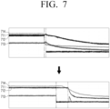
- FIG. 7 is a diagram for explaining an off sequence operation according to one or more embodiments.
- the off sequence information of the driver 120 is information for controlling the reset signal 711 to reach the low state first before the first driving signal V_DD 712 and the second driving signal V_LED 714.
- the processor 140 may detect a signal (V sense) 713 output from the power supply device 130 to thus control for the reset signal 711 among the plurality of signals 711, 712, and 714 to be in the low state first before the first driving signal V_DD 712 and the second driving signal V_LED 714.
- the processor 140 may control the reset signal 711 to be in the low state first as soon as detecting the low state of the signal (V sense) 713 output from the power supply device 130, and then control the first driving signal V_DD 712 to be in the low state for the second driving signal V_LED 714 to correspond to the off sequence information of the driver 120. That is, the processor 140 may first control the reset signal 711 to be in the low state based on off sequence information, and then control the power signal, that is, the first driving signal V_DD 712 and the second driving signal V_LED 714 to be in the low state.
- an interface signal transmitted to the driver 120 may include various signals based on implementation types of the driver 120, such as a Serial Peripheral Interface (SPI) signal, a CLK (clock) signal, and a Low-Voltage Differential Signaling (LVDS) signal.
- SPI Serial Peripheral Interface
- CLK clock
- LVDS Low-Voltage Differential Signaling
- FIGS. 8A and 8B are diagrams for respectively explaining the driving method of a display device according to one or more embodiments.
- a display device 100' may include the display panel 110, the driver 120, the power supply device 130, at least one processor 140, a communication interface 150, and a user interface 160.
- the description omits a detailed description of a component overlapping the component shown in FIG. 2 among the components shown in FIG. 8A .
- the communication interface 150 may be implemented as various interfaces based on an implementation example of the display device 100'.
- the communication interface 150 may communicate with the external device, an external storage medium (e.g., USB memory), an external server (e.g., a web hard) or the like by using a communication method such as a Bluetooth, an access point (AP) based wireless fidelity (Wi-Fi, i.e., wireless local area network (LAN)), a Zigbee, a wired/wireless local area network (LAN), a wide area network (WAN), Ethernet, an IEEE 1394, a high definition multimedia interface (HDMI), a universal serial bus (USB), a mobile high-definition link (MHL), an audio engineering society/European broadcasting union (AES/EBU) communication, an optical communication, or a coaxial communication.
- the communication interface 150 may communicate with another display device, the external server, and/or a remote control device, or the like.
- the user interface 160 may be implemented as a device such as a button, a touch pad, a mouse or a keyboard, or may be implemented as a touch screen or the like which may also perform a manipulation input function in addition to the above-described display function.
- the processor 140 may sequentially control the plurality of signals transmitted to at least one driver to be in the low state based on the off sequence information before the power is shut down. For example, in case of receiving a power-off remote control signal from the remote control device, the processor 140 may sequentially control the plurality of signals transmitted to at least one driver to be in the low state based on the off sequence information before power of the display device 100' is shut down.
- the processor 140 may receive the off signal through a micro controller unit (MCU) 810.
- MCU micro controller unit
- the power-off remote control signal received through the communication interface 150 may be processed through the MCU 810 and then transmitted to the processor 140.
- the processor 140 may sequentially control the plurality of signals transmitted to at least one driver to be in the low state based on the off sequence information before power of display device 100' is shut down based on the off signal transmitted from the MCU 810.
- the processor 140 may perform the same control operation based on an output signal of the power supply device 130, as well as the off signal received through the communication interface 150 and/or the user interface 160.
- a specific embodiment in which the plurality of signals transmitted to at least one driver are sequentially controlled to be in the low state based on the off sequence information is the same as those described with reference to FIGS. 1 to 7 , and its detailed description is thus omitted.
- FIG. 9 is a block diagram specifically showing a configuration of the display device according to one or more embodiments.
- a display device 100" may include the display panel 110, the driver 120, the power supply device 130, at least one processor 140, a communication interface 150, and a user interface 160, the memory 170, a speaker 180, and a camera 190.
- the description omits a detailed description of a component overlapping the component shown in FIGS. 2 and 8A among the component shown in FIG. 9 .
- the memory 170 may store data necessary for various embodiments.
- the memory 170 may be implemented as a memory embedded in the display device 100", or implemented as a memory detachable from the display device 100", based on a data storage purpose.
- data for driving the display device 100" may be stored in the memory embedded in the display device 100
- data for an extension function of the display device 100 may be stored in the memory detachable from the display device 100".
- the memory embedded in the display device 100" may be implemented as at least one of a volatile memory (for example, a dynamic random access memory (DRAM), a static RAM (SRAM), or a synchronous dynamic RAM (SDRAM)), a non-volatile memory (for example, an one time programmable read only memory (OTPROM), a programmable ROM (PROM), an erasable and programmable ROM (EPROM), an electrically erasable and programmable ROM (EEPROM), a mask ROM, or a flash ROM, a flash memory (for example, a NAND flash or a NOR flash), a hard drive, or a solid state drive (SSD)).
- a volatile memory for example, a dynamic random access memory (DRAM), a static RAM (SRAM), or a synchronous dynamic RAM (SDRAM)
- a non-volatile memory for example, an one time programmable read only memory (OTPROM), a programmable ROM (PROM), an erasable
- the memory detachable from the display device 100" may be implemented in the form of a memory card (for example, a compact flash (CF), a secure digital (SD), a micro secure digital (Micro-SD), a mini secure digital (Mini-SD), an extreme digital (xD), or a multi-media card (MMC)), or an external memory which may be connected to a USB port (for example, the USB memory).
- a memory card for example, a compact flash (CF), a secure digital (SD), a micro secure digital (Micro-SD), a mini secure digital (Mini-SD), an extreme digital (xD), or a multi-media card (MMC)
- CF compact flash
- SD secure digital
- Micro-SD micro secure digital
- Mini-SD mini secure digital
- xD extreme digital
- MMC multi-media card
- the memory 170 may store various data necessary for an operation of the display device 100".
- the memory 170 may store the power ON/Off sequence information required for each driver IC.
- the information stored in the memory 170 may not be stored in the memory 170, and may be acquired from an external device.
- some information may be received in real time from the external device such as a set-top box, the external server, or a user terminal.
- the memory 170 may store current information of the plurality of display modules 110-1 to 110-n.
- the current information may be current control information based on the luminance of each subpixel included in the display module.
- the current control information based on the luminance of each subpixel may be the current control information based on the luminance of each subpixel calibrated (or modeled) based on a luminance feature and a color shift feature based on the current of each subpixel.
- the speaker 180 may be a component outputting not only various audio data but also various notification sounds, voice messages, or the like.
- the processor 140 may control the speaker 180 to output feedbacks or various notifications in audio forms according to various embodiments of the present disclosure.
- the camera 190 may be turned on based on a predetermined event and perform a capture.
- the camera 190 may convert a captured image to an electrical signal and generate image data based on the converted signal.
- an object may be converted to an electrical image signal through a charge coupled device (CCD), and the converted image signal may be amplified and converted to a digital signal and then signal-processed.
- the camera 190 may be implemented as a general camera, a stereo camera, a depth camera.
- the display device 100" may include a sensor, a microphone, a tuner, and a demodulator, based on its implementation example.
- the sensor may include various types of sensors, such as the touch sensor, a proximity sensor, an acceleration sensor (or a gravity sensor), a geomagnetic sensor, a gyro sensor, a pressure sensor, a position sensor, a distance sensor, or a light sensor.
- sensors such as the touch sensor, a proximity sensor, an acceleration sensor (or a gravity sensor), a geomagnetic sensor, a gyro sensor, a pressure sensor, a position sensor, a distance sensor, or a light sensor.
- the microphone is a component for receiving a user voice or another sound and converting the user voice or another sound to the audio data.
- the display device 100" may receive the user voice input through the external device through the communication interface 150.
- the tuner may receive a radio frequency (RF) broadcast signal by tuning a channel selected by a user or all pre-stored channels among the RF broadcast signals received through an antenna.
- RF radio frequency
- the demodulator may receive and demodulate a digital intermediate frequency (DIF) signal converted by the tuner, and also perform channel decoding or the like.
- DIF digital intermediate frequency
- the processor 140 may detect the output voltage of the power supply device to thus control the signal based on the off sequence of the driver IC before the shutdown due to the AC power-off to prevent the screen transient.
- the various embodiments of the present disclosure described above may be performed through an embedded server disposed in the electronic device, or a server disposed outside the electronic device.
- the various embodiments described above may be implemented in software including an instruction stored in a machine-readable storage medium (for example, a computer-readable storage medium).
- the machine may be a device that invokes the stored instruction from the storage medium, may be operated based on the invoked instruction, and may include the electronic device (e.g., electronic device A) according to the disclosed embodiments.
- the instruction is executed by the processor, the processor may perform a function corresponding to the instruction directly or by using other components under control of the processor.
- the instruction may include a code provided or executed by a compiler or an interpreter.
- the machine-readable storage medium may be provided in the form of a non-transitory storage medium.
- the term "non-transitory" indicates that the storage medium is tangible without including a signal, and does not distinguish whether data are semi-permanently or temporarily stored in the storage medium.
- the method according to the various embodiments described above may be included and provided in a computer program product.
- the computer program product may be traded as a product between a seller and a purchaser.
- the computer program product may be distributed in a form of the machine-readable storage medium (for example, a compact disc read only memory (CD-ROM)), or may be distributed online through an application store (for example, PlayStore TM ).
- an application store for example, PlayStore TM
- at least a part of the computer program product may be at least temporarily stored or temporarily provided in a storage medium such as a memory of a server of a manufacturer, a server of an application store or a relay server.
- each of the components may include one entity or a plurality of entities, and some of the corresponding sub-components described above may be omitted or other sub-components may be further included in the various embodiments.
- some of the components e.g., modules or programs
Landscapes
- Engineering & Computer Science (AREA)
- Theoretical Computer Science (AREA)
- Physics & Mathematics (AREA)
- General Physics & Mathematics (AREA)
- General Engineering & Computer Science (AREA)
- Computer Hardware Design (AREA)
- Multimedia (AREA)
- Human Computer Interaction (AREA)
- Control Of Indicators Other Than Cathode Ray Tubes (AREA)
Applications Claiming Priority (2)
| Application Number | Priority Date | Filing Date | Title |
|---|---|---|---|
| KR1020230094534A KR20250014471A (ko) | 2023-07-20 | 2023-07-20 | 디스플레이 장치 그 구동 방법 |
| PCT/KR2024/004974 WO2025018517A1 (ko) | 2023-07-20 | 2024-04-12 | 디스플레이 장치 그 구동 방법 |
Publications (2)
| Publication Number | Publication Date |
|---|---|
| EP4524944A1 true EP4524944A1 (de) | 2025-03-19 |
| EP4524944A4 EP4524944A4 (de) | 2025-11-19 |
Family
ID=91030000
Family Applications (1)
| Application Number | Title | Priority Date | Filing Date |
|---|---|---|---|
| EP24719449.1A Pending EP4524944A4 (de) | 2023-07-20 | 2024-04-12 | Anzeigevorrichtung und verfahren zur ansteuerung davon |
Country Status (5)
| Country | Link |
|---|---|
| US (1) | US20260051286A1 (de) |
| EP (1) | EP4524944A4 (de) |
| KR (1) | KR20250014471A (de) |
| CN (1) | CN121014071A (de) |
| WO (1) | WO2025018517A1 (de) |
Family Cites Families (10)
| Publication number | Priority date | Publication date | Assignee | Title |
|---|---|---|---|---|
| JP4269582B2 (ja) * | 2002-05-31 | 2009-05-27 | ソニー株式会社 | 液晶表示装置およびその制御方法、ならびに携帯端末 |
| KR100497236B1 (ko) * | 2003-10-09 | 2005-06-23 | 삼성에스디아이 주식회사 | 플라즈마 디스플레이 패널의 전원 제어 장치 및 그 방법 |
| US20060181498A1 (en) * | 2003-12-24 | 2006-08-17 | Sony Corporation | Display device |
| US7459903B1 (en) * | 2007-11-26 | 2008-12-02 | Inventec Corporation | Multi-level voltage detection circuit |
| KR20140017392A (ko) * | 2012-08-01 | 2014-02-11 | 삼성전자주식회사 | 디스플레이장치 및 그 전원오류 검출방법 |
| DE102012024520B4 (de) * | 2012-09-28 | 2017-06-22 | Lg Display Co., Ltd. | Organische lichtemittierende Anzeige und Verfahren zum Entfernen eines Bildverbleibs von derselben |
| CN204131216U (zh) * | 2014-10-14 | 2015-01-28 | 山东超越数控电子有限公司 | 一种利用atx电源实现电源冗余备份的自动切换装置 |
| KR102534048B1 (ko) * | 2018-07-24 | 2023-05-18 | 주식회사 디비하이텍 | 소스 드라이버 및 이를 포함하는 디스플레이 장치 |
| KR102518436B1 (ko) * | 2018-10-22 | 2023-04-05 | 삼성전자주식회사 | 디스플레이 장치 및 그 제어 방법 |
| CN109192177B (zh) * | 2018-11-14 | 2023-03-17 | 维沃移动通信有限公司 | 一种控制电路、液晶显示驱动模组及液晶显示装置 |
-
2023
- 2023-07-20 KR KR1020230094534A patent/KR20250014471A/ko active Pending
-
2024
- 2024-04-12 WO PCT/KR2024/004974 patent/WO2025018517A1/ko active Pending
- 2024-04-12 CN CN202480026914.7A patent/CN121014071A/zh active Pending
- 2024-04-12 EP EP24719449.1A patent/EP4524944A4/de active Pending
-
2025
- 2025-10-27 US US19/370,092 patent/US20260051286A1/en active Pending
Also Published As
| Publication number | Publication date |
|---|---|
| CN121014071A (zh) | 2025-11-25 |
| EP4524944A4 (de) | 2025-11-19 |
| US20260051286A1 (en) | 2026-02-19 |
| KR20250014471A (ko) | 2025-02-03 |
| WO2025018517A1 (ko) | 2025-01-23 |
Similar Documents
| Publication | Publication Date | Title |
|---|---|---|
| CN111627406B (zh) | 显示装置、包括该显示装置的电子设备以及操作该电子设备的方法 | |
| US9740046B2 (en) | Method and apparatus to provide a lower power user interface on an LCD panel through localized backlight control | |
| US10545607B2 (en) | Pixel circuit and driving method, display panel and display apparatus | |
| US11128908B2 (en) | Electronic device and method for controlling the same | |
| CN101826316B (zh) | 在显示器的屏幕上显示内容的方法和系统 | |
| WO2015053569A1 (en) | Display driving circuit, display device, and portable terminal including the display driving circuit and the display device | |
| US20170038894A1 (en) | Display driver integrated circuit and electronic apparatus including the same | |
| CN108062933A (zh) | 显示设备和显示方法 | |
| US20240411428A1 (en) | Electronic apparatus and ui providing method thereof | |
| TWI718913B (zh) | 顯示方法 | |
| US20170025094A1 (en) | Display apparatus and display method | |
| KR20180065495A (ko) | 전원부 및 이를 포함하는 표시장치 | |
| EP4131241B1 (de) | Anzeigevorrichtung und elektronische vorrichtung | |
| EP4524944A1 (de) | Anzeigevorrichtung und verfahren zur ansteuerung davon | |
| CN110910839A (zh) | 显示模组的控制方法及控制系统 | |
| KR20230081246A (ko) | 디스플레이 장치 그 제어 방법 | |
| US12333203B2 (en) | Display apparatus, modular display apparatus and control method thereof | |
| US10896660B2 (en) | Display control device, display device, and display control method | |
| CN115547256A (zh) | 驱动电路及其驱动方法、电子设备以及显示装置 | |
| KR102466286B1 (ko) | 터치표시장치 및 그 구동방법 | |
| US20250094113A1 (en) | Display apparatus for identifying connection and disconnection of external display device and control method thereof | |
| CN119446058A (zh) | 电子装置 | |
| KR20260005472A (ko) | 전자 장치 및 그 제어 방법 | |
| KR20250128867A (ko) | 디스플레이 드라이버와 이를 포함한 표시장치 | |
| CN121219763A (zh) | 用于电子设备的分层显示器 |
Legal Events
| Date | Code | Title | Description |
|---|---|---|---|
| STAA | Information on the status of an ep patent application or granted ep patent |
Free format text: STATUS: UNKNOWN |
|
| STAA | Information on the status of an ep patent application or granted ep patent |
Free format text: STATUS: THE INTERNATIONAL PUBLICATION HAS BEEN MADE |
|
| PUAI | Public reference made under article 153(3) epc to a published international application that has entered the european phase |
Free format text: ORIGINAL CODE: 0009012 |
|
| STAA | Information on the status of an ep patent application or granted ep patent |
Free format text: STATUS: REQUEST FOR EXAMINATION WAS MADE |
|
| 17P | Request for examination filed |
Effective date: 20240425 |
|
| AK | Designated contracting states |
Kind code of ref document: A1 Designated state(s): AL AT BE BG CH CY CZ DE DK EE ES FI FR GB GR HR HU IE IS IT LI LT LU LV MC ME MK MT NL NO PL PT RO RS SE SI SK SM TR |
|
| A4 | Supplementary search report drawn up and despatched |
Effective date: 20251022 |
|
| RIC1 | Information provided on ipc code assigned before grant |
Ipc: G09G 3/32 20160101AFI20251016BHEP Ipc: G09F 9/302 20060101ALI20251016BHEP Ipc: G06F 1/26 20060101ALI20251016BHEP Ipc: G06F 1/28 20060101ALI20251016BHEP Ipc: G06F 1/30 20060101ALI20251016BHEP |