EP4523836A1 - Laser etching device, laser etching system, electrode etched using laser, and method for manufacturing same electrode - Google Patents
Laser etching device, laser etching system, electrode etched using laser, and method for manufacturing same electrode Download PDFInfo
- Publication number
- EP4523836A1 EP4523836A1 EP23824094.9A EP23824094A EP4523836A1 EP 4523836 A1 EP4523836 A1 EP 4523836A1 EP 23824094 A EP23824094 A EP 23824094A EP 4523836 A1 EP4523836 A1 EP 4523836A1
- Authority
- EP
- European Patent Office
- Prior art keywords
- active material
- laser
- material portion
- unit
- laser etching
- Prior art date
- Legal status (The legal status is an assumption and is not a legal conclusion. Google has not performed a legal analysis and makes no representation as to the accuracy of the status listed.)
- Pending
Links
Images




Classifications
-
- B—PERFORMING OPERATIONS; TRANSPORTING
- B08—CLEANING
- B08B—CLEANING IN GENERAL; PREVENTION OF FOULING IN GENERAL
- B08B15/00—Preventing escape of dirt or fumes from the area where they are produced; Collecting or removing dirt or fumes from that area
- B08B15/04—Preventing escape of dirt or fumes from the area where they are produced; Collecting or removing dirt or fumes from that area from a small area, e.g. a tool
-
- B—PERFORMING OPERATIONS; TRANSPORTING
- B23—MACHINE TOOLS; METAL-WORKING NOT OTHERWISE PROVIDED FOR
- B23K—SOLDERING OR UNSOLDERING; WELDING; CLADDING OR PLATING BY SOLDERING OR WELDING; CUTTING BY APPLYING HEAT LOCALLY, e.g. FLAME CUTTING; WORKING BY LASER BEAM
- B23K26/00—Working by laser beam, e.g. welding, cutting or boring
- B23K26/36—Removing material
- B23K26/362—Laser etching
-
- B—PERFORMING OPERATIONS; TRANSPORTING
- B08—CLEANING
- B08B—CLEANING IN GENERAL; PREVENTION OF FOULING IN GENERAL
- B08B5/00—Cleaning by methods involving the use of air flow or gas flow
- B08B5/02—Cleaning by the force of jets, e.g. blowing-out cavities
-
- B—PERFORMING OPERATIONS; TRANSPORTING
- B23—MACHINE TOOLS; METAL-WORKING NOT OTHERWISE PROVIDED FOR
- B23K—SOLDERING OR UNSOLDERING; WELDING; CLADDING OR PLATING BY SOLDERING OR WELDING; CUTTING BY APPLYING HEAT LOCALLY, e.g. FLAME CUTTING; WORKING BY LASER BEAM
- B23K26/00—Working by laser beam, e.g. welding, cutting or boring
- B23K26/14—Working by laser beam, e.g. welding, cutting or boring using a fluid stream, e.g. a jet of gas, in conjunction with the laser beam; Nozzles therefor
- B23K26/142—Working by laser beam, e.g. welding, cutting or boring using a fluid stream, e.g. a jet of gas, in conjunction with the laser beam; Nozzles therefor for the removal of by-products
-
- B—PERFORMING OPERATIONS; TRANSPORTING
- B23—MACHINE TOOLS; METAL-WORKING NOT OTHERWISE PROVIDED FOR
- B23K—SOLDERING OR UNSOLDERING; WELDING; CLADDING OR PLATING BY SOLDERING OR WELDING; CUTTING BY APPLYING HEAT LOCALLY, e.g. FLAME CUTTING; WORKING BY LASER BEAM
- B23K26/00—Working by laser beam, e.g. welding, cutting or boring
- B23K26/16—Removal of by-products, e.g. particles or vapours produced during treatment of a workpiece
-
- H—ELECTRICITY
- H01—ELECTRIC ELEMENTS
- H01M—PROCESSES OR MEANS, e.g. BATTERIES, FOR THE DIRECT CONVERSION OF CHEMICAL ENERGY INTO ELECTRICAL ENERGY
- H01M4/00—Electrodes
- H01M4/02—Electrodes composed of, or comprising, active material
- H01M4/04—Processes of manufacture in general
-
- H—ELECTRICITY
- H01—ELECTRIC ELEMENTS
- H01M—PROCESSES OR MEANS, e.g. BATTERIES, FOR THE DIRECT CONVERSION OF CHEMICAL ENERGY INTO ELECTRICAL ENERGY
- H01M4/00—Electrodes
- H01M4/02—Electrodes composed of, or comprising, active material
- H01M4/04—Processes of manufacture in general
- H01M4/0402—Methods of deposition of the material
- H01M4/0404—Methods of deposition of the material by coating on electrode collectors
-
- H—ELECTRICITY
- H01—ELECTRIC ELEMENTS
- H01M—PROCESSES OR MEANS, e.g. BATTERIES, FOR THE DIRECT CONVERSION OF CHEMICAL ENERGY INTO ELECTRICAL ENERGY
- H01M4/00—Electrodes
- H01M4/02—Electrodes composed of, or comprising, active material
- H01M4/04—Processes of manufacture in general
- H01M4/0471—Processes of manufacture in general involving thermal treatment, e.g. firing, sintering, backing particulate active material, thermal decomposition, pyrolysis
-
- B—PERFORMING OPERATIONS; TRANSPORTING
- B08—CLEANING
- B08B—CLEANING IN GENERAL; PREVENTION OF FOULING IN GENERAL
- B08B7/00—Cleaning by methods not provided for in a single other subclass or a single group in this subclass
- B08B7/0035—Cleaning by methods not provided for in a single other subclass or a single group in this subclass by radiant energy, e.g. UV, laser, light beam or the like
- B08B7/0042—Cleaning by methods not provided for in a single other subclass or a single group in this subclass by radiant energy, e.g. UV, laser, light beam or the like by laser
-
- B—PERFORMING OPERATIONS; TRANSPORTING
- B23—MACHINE TOOLS; METAL-WORKING NOT OTHERWISE PROVIDED FOR
- B23K—SOLDERING OR UNSOLDERING; WELDING; CLADDING OR PLATING BY SOLDERING OR WELDING; CUTTING BY APPLYING HEAT LOCALLY, e.g. FLAME CUTTING; WORKING BY LASER BEAM
- B23K2101/00—Articles made by soldering, welding or cutting
- B23K2101/36—Electric or electronic devices
- B23K2101/38—Conductors
-
- Y—GENERAL TAGGING OF NEW TECHNOLOGICAL DEVELOPMENTS; GENERAL TAGGING OF CROSS-SECTIONAL TECHNOLOGIES SPANNING OVER SEVERAL SECTIONS OF THE IPC; TECHNICAL SUBJECTS COVERED BY FORMER USPC CROSS-REFERENCE ART COLLECTIONS [XRACs] AND DIGESTS
- Y02—TECHNOLOGIES OR APPLICATIONS FOR MITIGATION OR ADAPTATION AGAINST CLIMATE CHANGE
- Y02E—REDUCTION OF GREENHOUSE GAS [GHG] EMISSIONS, RELATED TO ENERGY GENERATION, TRANSMISSION OR DISTRIBUTION
- Y02E60/00—Enabling technologies; Technologies with a potential or indirect contribution to GHG emissions mitigation
- Y02E60/10—Energy storage using batteries
Definitions
- the present invention relates to a laser etching device, a laser etching system, an electrode etched using a laser, and a method for manufacturing the electrode.
- the secondary batteries undergo various processes in a manufacturing process.
- the secondary batteries are produced through processes such as an electrode process, an assembly process, and a chemical process.
- an active material is applied in a predetermined pattern on an electrode sheet, and techniques for raw material mixing conditions, temperature, and process conditions of the coating device are proposed for managing coating quality.
- An object of the present invention for solving the above problem is to provide a laser etching device capable of improving coating quality of an active material through etching using a laser, a laser etching system, an electrode etched using a laser, and a method for manufacturing the electrode.
- a laser etching device which etches an active material portion on an electrode sheet including the active material portion and a non-coating portion, according to an embodiment of the present invention includes a laser unit configured to irradiate laser onto the active material portion, a blowing unit configured to blow foreign substances generated by the etching of the active material portion toward the non-coating portion, and a suction unit disposed at an opposite side of the blowing unit with the laser unit therebetween to suction the foreign substances, wherein the laser unit, the blowing unit, and the suction unit are disposed in a direction traversing a moving direction of the electrode sheet.
- a laser etching system which etches a first active material portion and a second active material portion on an electrode sheet including the first active material portion, the second active material portion, and a non-coating portion disposed between the first active material portion and the second active material portion, according to an embodiment of the present invention includes a first laser etching device configured to etch the first active material portion, and a second laser etching device configured to etch the second active material portion, wherein each of the first laser etching device and the second laser etching device includes a laser unit configured to irradiate laser onto the active material portion, a blowing unit configured to blow foreign substances generated by the etching of the active material portion toward the non-coating portion, and a suction unit disposed at an opposite side of the blowing unit with the laser unit therebetween to suction the foreign substances, wherein the laser unit, the blowing unit, and the suction unit are disposed in a direction traversing a moving direction of the electrode sheet.
- An electrode according to an embodiment of the present invention includes an active material portion coated with an active material on an electrode sheet, and a non-coating portion on which the active material is not applied on the electrode sheet, wherein a heat-affected zone (HAZ) having a width of 200 ⁇ m or less is defined on a boundary between the active material portion and the non-coating portion.
- HZ heat-affected zone
- a method for manufacturing an electrode according to an embodiment of the present invention includes applying an active material on an electrode sheet to form an active material portion and a non-coating portion, and etching a portion of an edge of the active material portion, wherein the etching of the portion of the edge includes irradiating laser to the portion of the edge using a laser unit to etch the portion of the edge, blowing foreign substances generated by etching the portion of the edge toward the non-coating portion using a blowing unit, and suctioning the foreign substances blown and diffused by using a suction unit disposed at an opposite side of the blowing unit with the laser unit therebetween.
- the coating quality of the active material may be improved in the electrode process.
- the diffusion of the foreign substances caused by the etching may be effectively prevented.
- FIG. 1 is a schematic view illustrating an example of applying an active material on an electrode sheet 10.
- a process of applying the active material on the electrode sheet 10 may be performed.
- the active material may be applied on the electrode sheet (or electrode current collector) in a predetermined pattern, and an active material portion, on which the active material is applied, and a non-coating portion 30, on which the active material is not applied, may be provided on the electrode sheet 10.
- the active material portion 20 may include an active material portion 20 having a regular arrangement through the predetermined pattern of the active material coating (stripe coating) on the electrode sheet 10.
- the non-coating portion 30 may be disposed between the active material portions 20.
- the predetermined pattern is not limited to the stripe coating and also may be intermittent coating and may not be particularly limited.
- FIGS. 2 and 3 are schematic view of an area to which etching is applicable when the active material is applied on the electrode sheet 10 according to embodiments of the present invention.
- FIG. 2 is a side view of the electrode sheet 10
- FIG. 3 is a plan view of the electrode sheet 10. The above description may be equally or similarly applied below.
- the active material may be applied on both surfaces of the electrode sheet 10.
- the active material may be applied on a top surface of the electrode sheet 10 to provide an upper active material portion 21, and the active material may be applied on a bottom surface of the electrode sheet 10 to provide a lower active material portion 22.
- sliding may occur during the coating of the upper active material portion 21, and mismatching with the lower active material portion 22 may occur.
- etching may be required on a boundary area 11 that is an edge area of the upper active material portion 21. Also, unlike that illustrated in FIG.
- the sliding may occur at the lower active material portion 22, and thus, the mismatching with the upper active material portion 21 may occur.
- the etching of the edge area of the lower active material portion 22 may be required to solve the mismatching.
- the edge area may be a boundary area between the active material portions 21 and 22 and the non-coating portion (e.g., the non-coating portion 30).
- a plurality of active material portions 20a, 20b, and 20c may be provided on the electrode sheet 10.
- FIG. 3 illustrates that the active material portions 20a, 20b, and 20c are provided in a stripe pattern, the following description is not limited thereto.
- Each of the first active material portion 20a, the second active material portion 20b, and the third active material portion 20c may be coated in the stripe pattern in parallel on the electrode sheet 10.
- the coated first active material portion 20a, second active material portion 20b, and third active material portion 20c may require etching to a degree required for a subsequent process (e.g., a notching process).
- etching of a preliminary notching area 12 may be required during the coating process.
- notching may be performed on a portion of the preliminary notching area 12 to form the electrode tab.
- the boundary area 11 and the preliminary notching area 12 have been described with reference to FIGS. 2 and 3 , the area on which the etching is required may not be limited thereto, and the following description will be given in the area on which the etching is required. In the case of performing the etching, it may be applied without particular limitation.
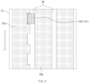
- FIG. 4 is a schematic view of the laser etching system 100 according to an embodiment of the present invention. The above description may be equally or similarly applied below.
- the laser etching system 100 may perform laser etching on an area, on which the etching is required, such as the boundary area 11 or the preliminary notching area 12.
- the laser etching system 100 may include a laser etching device 101, and the active material portion (e.g., the first active material portion 20a) may be etched using the laser etching device 101.
- the laser etching device 101 may etch an edge of the first active material portion 20a at a predetermined position in a traveling direction of the electrode sheet 10. While the electrode sheet 10 moves along the traveling direction, the etching may be performed by a predetermined area at predetermined intervals by the laser etching device 101.
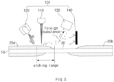
- FIG. 5 is a schematic view illustrating the laser etching device 101 of the laser etching system 100 and a state in which the laser etching device 101 etches a first active material portion 20a according to an embodiment of the present invention
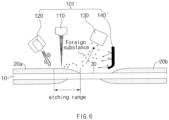
- FIG. 6 is a schematic view illustrating a laser etching device 101' that is a modified example of the laser etching device illustrated in FIG. 5 .
- the above description may be equally or similarly applied below.
- the first active material portion 20a has been described below as an example, it is not particularly limited.
- the active material portions 20a, 20b, and 20c may be applied on the electrode sheet 10, and the laser etching device 101 may perform etching on the first active material portion 20a.
- the laser etching device 101 etches the first active material portion 20a will be described, but is not limited thereto.
- the laser etching device 101 may include at least a laser unit 110, a blowing unit 120 and a suction unit 130.
- the laser unit 110, the blowing unit 120, and the suction unit 130 of the laser etching device 101 may be disposed in a direction traversing the traveling direction (or moving direction) of the electrode sheet 10.
- the laser unit 110 may be disposed on the edge of the first active material portion 20a to radiate laser to the edge of the first active material portion 20a.
- the blowing unit 120 may be disposed on the first active material portion 20a to blow the foreign substances in a direction from the first active material portion 20a to the second active material portion 20b.
- the blowing unit 120 may be disposed inside the first active material portion 20a rather than the laser unit 110.
- the blowing unit 120 may be disposed farther from the edge of the first active material portion 20a than the laser unit 110.
- the suction unit 130 may be disposed at an opposite side of the blowing unit 120 with respect to the laser unit 110.
- the suction unit 130 may be disposed on the non-coating portion 30 or the second active material portion 20b.
- the foreign substances blown by the blower unit 120 may be effectively prevented from being accumulated on an etching target again.
- the foreign substances of the first active material portion 20a blown by the blowing unit 120 may be prevented from being accumulated on the first active material portion 20a again.
- the laser etching device 101 further includes the barrier 140, it is possible to prevent not only the above-described effect but also an influence of the neighboring active material portion.
- the foreign substances of the first active material portion 20a blown by the blowing unit 120 through the barrier 140 may be prevented from being accumulated on the second active material portion 20b.
- a laser etching device 101' which is a modified example of the laser etching device 101, may include a barrier 140'.
- the barrier 140' may include a bent portion.
- the barrier 140' may include a portion extending in a direction perpendicular to the electrode sheet 10 (or the top surface of the electrode sheet 10), and the barrier 140' may include a bent portion bent from a distal end of a side of the electrode sheet 10 toward the non-coating portion 30 or the suction unit 130.
- the barrier 140' includes the bent portion, it is possible to block the foreign substances diffused in a diagonal direction.
- the diffusion of the foreign substances may be effectively prevented by preventing the foreign substances blown by the blowing unit 120 from moving in the diagonal direction with respect to the second active material portion 20b.
- a blowing path (or air flow) by the blowing unit 120 may be guided.
- the suction of the suction unit 130 may be more effective by guiding the air blowing path so that the air flow is directed toward the suction unit 130.
- the barriers 140 and 140' described with reference to FIGS. 5 and 6 may be disposed above the other active material portion adjacent to one active material portion that is subjected to the etching.
- the barriers 140 and 140' may be disposed above the second active material portion 20b that is the other active material portion adjacent with the first active material portion 20a, which is one active material portion etched by the laser unit 110, and the non-coating portion 30 therebetween.
- the second active material portion 20b may be disposed above the edge of the non-coated portion 30 so as not to diffuse the foreign substances into the second active material portion 20b.
- the barriers 140 and 140' may be disposed above the non-coating portion 30.
- the barriers 140 and 140' are disposed above the non-coating portion 30, but may be disposed on the non-coating portion 30 at a side of the second active material portion 20b.
- the barriers 140 and 140' may be disposed closer to the other active material portion adjacent to one active material portion than to one active material portion on which the etching is performed. For example, a distance between the first active material portion 20a, which is one active material portion etched by the laser unit 110, and each of the barriers 140 and 140' may be greater than a distance between the second active material portion 20b, which is the other active material portion adjacent with the first active material portion 20a and the non-coating portion 30 therebetween, and each of the barriers 140 and 140'.
- the barriers 140 and 140' may be disposed closer to the second active material portion 20b than the suction unit 130.
- the distance between each of the barriers 140 and 140' and the second active material unit may be less than a distance between the suction unit 130 and the second active material portion 20b to prevent the foreign substances, which are blown by the blowing unit 120, but are not suctioned by the suction unit 130, from being diffused into the second active material portion 20b.
- the electrode may be manufactured by etching the first active material portion 20a using the laser etching device 101.
- a process of etching the first active material portion 20a using the laser etching device 101 has been described, but may be equally or similarly applied in processes of etching the second active material portion 20b using the laser etching device 102 to be described later.
- the method for manufacturing the electrode may include a process of applying the active material on the electrode sheet 10 to form the active material portions 20a and 20b and the non-coating portion 30.
- the method for manufacturing the electrode may include a process of etching a portion of the edge of the first active material portion 20a.
- the etching process may include a process of irradiating laser to a portion of the edge of the first active material portion 20a using the laser unit 110 to etch the portion of the edge of the first active material portion 20a, a process of blowing air toward the non-coating portion 30 using the blowing unit 120 for foreign substances generated as the portion of the edge is etched, and a process of suctioning the foreign substances blown and diffused by using the suction unit 130 disposed at the opposite side of the blowing unit 120 with the laser unit 110 therebetween.
- the portion of the edge may be a portion of a boundary between the first active material portion 20a and the non-coating portion 30.
- FIG. 7 is a schematic view of a laser etching system 100' according to another embodiment of the present invention.
- the laser etching system 100' may include laser etching devices 101 and 102. The above description may be equally or similarly applied below.
- the laser etching system 100' may include a laser etching device 101 and a laser etching device 102.
- the laser etching device 101 and the laser etching device 102 may be sequentially disposed in a moving direction (or traveling direction) of the electrode sheet 10.
- the laser etching device 101 and the laser etching device 102 may be disposed in the traveling direction of the electrode sheet 10 (e.g., direction indicated by an arrow) and may be spaced a predetermined distance from each other in the traveling direction.
- the laser etching device 101 may be disposed adjacent to the first active material portion 20a to perform the etching on the first active material portion 20a, and the laser etching device 102 may be disposed adjacent to the second active material portion 20b to perform the etching on the second active material portion 20b.
- the laser etching device 101 may etch the edge of the first active material portion 20a, which is defined as a boundary with the non-coating portion 30, and the laser etching device 102 may etch the second active material portion 20b, which is defined as a boundary with the non-coating portion 30.
- the laser etching device 101 and the laser etching device 102 may be disposed at predetermined positions to perform the etching on the edge of each of the first active material portion 20a and the second active material portion 20b while the electrode sheet 10 moves in the traveling direction.
- the edge may be a boundary between the active material portions 20a and 20b and the non-coating portion 30.
- FIG. 8 is a view illustrating a state in which a laser etching device 102 of the laser etching system 100' etches the second active material portion 20b according to another embodiment of the present invention.
- the above description may be equally or similarly applied below.
- the laser etching device 102 may include a laser unit 210, a blowing unit 220, a suction unit 230, and a barrier 240, which respectively correspond to the laser unit 110, the blowing unit 120, the suction unit 130, and the barrier 140 of the above-described laser etching device 101.
- the barrier 240 may correspond to the barrier 140' of the laser etching device 101', which is a modified example of the laser etching device 101.
- the laser unit 210, the blowing unit 220, the suction unit 230, and the barrier 240 may be disposed in a direction that is symmetrical to the laser etching devices 101 and 101' to perform the etching on the second active material portion 20b.
- the same or similar descriptions may be applied to the arrangement positions and operations of the laser unit 210, the blowing unit 220, the suction unit 230, and the barrier 240.
- FIG. 9 is a view illustrating a heat-affected zone defined at a boundary between the active material portion 20a and a non-coating portion 30 according to embodiments of the present invention. The above description may be equally or similarly applied below.
- the electrode may include a first active material portion 20a coated with the active material on the electrode sheet 10 and a non-coating portion 30 on which the active material is not applied on the electrode sheet 10.
- the boundary between the laser-etched first active material portion 20a and the non-coating portion 30 (or an edge of the first active material portion 20a) may define a portion of the electrode.
- the heat affected zone (HAZ) 400 may be defined at the boundary between the first active material portion 20a and the non-coating portion 30 by the laser etching.
- the heat-affected zone 400 may have brightness less than that the non-coating portion 30.
- the heat-affected zone 400 may preferably have a width of 200 ⁇ m or less.
Landscapes
- Engineering & Computer Science (AREA)
- Physics & Mathematics (AREA)
- Optics & Photonics (AREA)
- Plasma & Fusion (AREA)
- Mechanical Engineering (AREA)
- Manufacturing & Machinery (AREA)
- Chemical & Material Sciences (AREA)
- Chemical Kinetics & Catalysis (AREA)
- Electrochemistry (AREA)
- General Chemical & Material Sciences (AREA)
- Battery Electrode And Active Subsutance (AREA)
- Laser Beam Processing (AREA)
Abstract
Description
- The present application claims the benefit of the priority of
Korean Patent Application Nos. 10-2022-0072395, filed on June 14, 2022 10-2023-0057012, filed on May 02, 2023 - The present invention relates to a laser etching device, a laser etching system, an electrode etched using a laser, and a method for manufacturing the electrode.
- In response to environmental pollution and depletion of petroleum resources, research and development on power generation based on Eco-friendly energy sources are being conducted. Particularly, research on secondary batteries is being actively conducted, and research is being conducted on various aspects such as materials, structures, processes, and systems of the secondary batteries.
- The secondary batteries undergo various processes in a manufacturing process. In general, the secondary batteries are produced through processes such as an electrode process, an assembly process, and a chemical process. In the above processes, in particular, in the electrode process, an active material is applied in a predetermined pattern on an electrode sheet, and techniques for raw material mixing conditions, temperature, and process conditions of the coating device are proposed for managing coating quality.
- According to the related art, when an active material is applied on an electrode sheet in a predetermined pattern, sliding or mismatch may occur at an edge of a coating area, and there is a concern that deterioration in performance and quality of the electrode assembly occurs due to deterioration in coating quality.
- An object of the present invention for solving the above problem is to provide a laser etching device capable of improving coating quality of an active material through etching using a laser, a laser etching system, an electrode etched using a laser, and a method for manufacturing the electrode.
- A laser etching device, which etches an active material portion on an electrode sheet including the active material portion and a non-coating portion, according to an embodiment of the present invention includes a laser unit configured to irradiate laser onto the active material portion, a blowing unit configured to blow foreign substances generated by the etching of the active material portion toward the non-coating portion, and a suction unit disposed at an opposite side of the blowing unit with the laser unit therebetween to suction the foreign substances, wherein the laser unit, the blowing unit, and the suction unit are disposed in a direction traversing a moving direction of the electrode sheet.
- A laser etching system, which etches a first active material portion and a second active material portion on an electrode sheet including the first active material portion, the second active material portion, and a non-coating portion disposed between the first active material portion and the second active material portion, according to an embodiment of the present invention includes a first laser etching device configured to etch the first active material portion, and a second laser etching device configured to etch the second active material portion, wherein each of the first laser etching device and the second laser etching device includes a laser unit configured to irradiate laser onto the active material portion, a blowing unit configured to blow foreign substances generated by the etching of the active material portion toward the non-coating portion, and a suction unit disposed at an opposite side of the blowing unit with the laser unit therebetween to suction the foreign substances, wherein the laser unit, the blowing unit, and the suction unit are disposed in a direction traversing a moving direction of the electrode sheet.
- An electrode according to an embodiment of the present invention includes an active material portion coated with an active material on an electrode sheet, and a non-coating portion on which the active material is not applied on the electrode sheet, wherein a heat-affected zone (HAZ) having a width of 200 µm or less is defined on a boundary between the active material portion and the non-coating portion.
- A method for manufacturing an electrode according to an embodiment of the present invention includes applying an active material on an electrode sheet to form an active material portion and a non-coating portion, and etching a portion of an edge of the active material portion, wherein the etching of the portion of the edge includes irradiating laser to the portion of the edge using a laser unit to etch the portion of the edge, blowing foreign substances generated by etching the portion of the edge toward the non-coating portion using a blowing unit, and suctioning the foreign substances blown and diffused by using a suction unit disposed at an opposite side of the blowing unit with the laser unit therebetween.
- According to the preferred embodiment of the present invention, the coating quality of the active material may be improved in the electrode process.
- According to the preferred embodiment of the present invention, even if the portion of the coated active material is managed through the etching, the diffusion of the foreign substances caused by the etching may be effectively prevented.
-
-
FIG. 1 is a schematic view illustrating an example of applying an active material on an electrode sheet. -
FIGS. 2 and3 are schematic view of an area to which etching is applicable when the active material is applied on the electrode sheet according to embodiments of the present invention. -
FIG. 4 is a schematic view of a laser etching system according to an embodiment of the present invention. -
FIG. 5 is a schematic view illustrating a laser etching device of a laser etching system and a state in which the laser etching device etches a first active material portion according to an embodiment of the present invention. -
FIG. 6 is a schematic view illustrating a modified example of the laser etching device illustrated inFIG. 5 . -
FIG. 7 is a schematic view of a laser etching system according to another embodiment of the present invention. -
FIG. 8 is a view illustrating a state in which a laser etching device of the laser etching system etches a second active material portion according to another embodiment of the present invention. -
FIG. 9 is a view illustrating a heat-affected zone defined at a boundary between the active material portion and a non-coating portion according to embodiments of the present invention. - Hereinafter, preferred embodiments of the present invention will be described in detail with reference to the accompanying drawings so that those of ordinary skill in the art can easily carry out the present invention. However, the present invention may be implemented in several different forms and is not limited or restricted by the following examples.
- In order to clearly explain the present invention, detailed descriptions of portions that are irrelevant to the description or related known technologies that may unnecessarily obscure the gist of the present invention have been omitted, and in the present specification, reference symbols are added to components in each drawing. In this case, the same or similar reference numerals are assigned to the same or similar elements throughout the specification.
- Also, terms or words used in this specification and claims should not be restrictively interpreted as ordinary meanings or dictionary-based meanings, but should be interpreted as meanings and concepts conforming to the scope of the present invention on the basis of the principle that an inventor can properly define the concept of a term to describe and explain his or her invention in the best ways.
-
FIG. 1 is a schematic view illustrating an example of applying an active material on anelectrode sheet 10. - In an electrode process of processes of producing a secondary battery, a process of applying the active material on the
electrode sheet 10 may be performed. The active material may be applied on the electrode sheet (or electrode current collector) in a predetermined pattern, and an active material portion, on which the active material is applied, and anon-coating portion 30, on which the active material is not applied, may be provided on theelectrode sheet 10. - As illustrated in
FIG. 1 , theactive material portion 20 may include anactive material portion 20 having a regular arrangement through the predetermined pattern of the active material coating (stripe coating) on theelectrode sheet 10. Thenon-coating portion 30 may be disposed between theactive material portions 20. The predetermined pattern is not limited to the stripe coating and also may be intermittent coating and may not be particularly limited. -
FIGS. 2 and3 are schematic view of an area to which etching is applicable when the active material is applied on theelectrode sheet 10 according to embodiments of the present invention.FIG. 2 is a side view of theelectrode sheet 10, andFIG. 3 is a plan view of theelectrode sheet 10. The above description may be equally or similarly applied below. - Referring to
FIG. 2 , the active material may be applied on both surfaces of theelectrode sheet 10. For example, the active material may be applied on a top surface of theelectrode sheet 10 to provide an upperactive material portion 21, and the active material may be applied on a bottom surface of theelectrode sheet 10 to provide a loweractive material portion 22. In this case, sliding may occur during the coating of the upperactive material portion 21, and mismatching with the loweractive material portion 22 may occur. When mismatching with the loweractive material portion 22 occurs due to the sliding during the coating of the upperactive material portion 21, in order to improve coating quality by solving the mismatching, etching may be required on aboundary area 11 that is an edge area of the upperactive material portion 21. Also, unlike that illustrated inFIG. 2 , the sliding may occur at the loweractive material portion 22, and thus, the mismatching with the upperactive material portion 21 may occur. In this case, the etching of the edge area of the loweractive material portion 22 may be required to solve the mismatching. The edge area may be a boundary area between theactive material portions - Referring to
FIG. 3 , a plurality ofactive material portions electrode sheet 10. AlthoughFIG. 3 illustrates that theactive material portions active material portion 20a, the secondactive material portion 20b, and the thirdactive material portion 20c may be coated in the stripe pattern in parallel on theelectrode sheet 10. The coated firstactive material portion 20a, secondactive material portion 20b, and thirdactive material portion 20c may require etching to a degree required for a subsequent process (e.g., a notching process). For example, when the notching process of forming an electrode tab is performed after applying the firstactive material portion 20a, the secondactive material portion 20b, and the thirdactive material portion 20c in the electrode process, etching of apreliminary notching area 12 may be required during the coating process. During the notching process, notching may be performed on a portion of thepreliminary notching area 12 to form the electrode tab. - Although the
boundary area 11 and thepreliminary notching area 12 have been described with reference toFIGS. 2 and3 , the area on which the etching is required may not be limited thereto, and the following description will be given in the area on which the etching is required. In the case of performing the etching, it may be applied without particular limitation. -
FIG. 4 is a schematic view of thelaser etching system 100 according to an embodiment of the present invention. The above description may be equally or similarly applied below. - The
laser etching system 100 may perform laser etching on an area, on which the etching is required, such as theboundary area 11 or thepreliminary notching area 12. Thelaser etching system 100 may include alaser etching device 101, and the active material portion (e.g., the firstactive material portion 20a) may be etched using thelaser etching device 101. For example, thelaser etching device 101 may etch an edge of the firstactive material portion 20a at a predetermined position in a traveling direction of theelectrode sheet 10. While theelectrode sheet 10 moves along the traveling direction, the etching may be performed by a predetermined area at predetermined intervals by thelaser etching device 101. - Hereinafter, the
laser etching device 101 of thelaser etching system 100 will be described in detail. -
FIG. 5 is a schematic view illustrating thelaser etching device 101 of thelaser etching system 100 and a state in which thelaser etching device 101 etches a firstactive material portion 20a according to an embodiment of the present invention, andFIG. 6 is a schematic view illustrating a laser etching device 101' that is a modified example of the laser etching device illustrated inFIG. 5 . The above description may be equally or similarly applied below. In addition, although the firstactive material portion 20a has been described below as an example, it is not particularly limited. - As described above, the
active material portions electrode sheet 10, and thelaser etching device 101 may perform etching on the firstactive material portion 20a. Hereinafter, an example in which thelaser etching device 101 etches the firstactive material portion 20a will be described, but is not limited thereto. - Referring to
FIGS. 5 and6 , thelaser etching device 101 may include alaser unit 110. Thelaser unit 110 may irradiate laser onto the firstactive material portion 20a. For example, thelaser unit 110 may irradiate laser onto the edge of the firstactive material portion 20a to etch the edge of the firstactive material portion 20a. When the laser is irradiated onto the firstactive material portion 20a, foreign substances (e.g., etched active material residue) may be generated by the laser etching. The edge may be a boundary between the firstactive material portion 20a and thenon-coating portion 30. - The
laser etching device 101 may include ablowing unit 120. Theblowing unit 120 may blow the foreign substances generated by etching the firstactive material portion 20a. For example, theblowing unit 120 may be disposed above the firstactive material portion 20a and may blow the air toward thenon-coating portion 30 for the foreign substances from an upper side of the firstactive material portion 20a. In this case, the foreign substances generated by the etching may fly toward thenon-coating portion 30 or the secondactive material portion 20b, which is directed in a direction away from the firstactive material portion 20a. Theblowing unit 120 may blow the air at a blowing angle of 10 degrees to 80 degrees based on an air-receiving surface of both surfaces of theelectrode sheet 10. When theblowing unit 120 blows the air at an angle greater than 80 degrees, the foreign substances may be blown onto the firstactive material portion 20a. In addition, when theblowing unit 120 blows air at an angle less than 10 degrees, asuction unit 130 to be described below may blow the foreign substances toward the secondactive material portion 20b before suctioning the foreign substances. In addition, an diffusion preventing effect by abarrier 140 described later may be reduced. The blowing angle of theblowing unit 120 may be an angle that is effective for thesuction unit 130 to suction the foreign substances generated due to the etching or may maximize the diffusion preventing effect by thebarrier 140. In addition, theblowing unit 120 may blow the air with a blowing pressure of 0.2 bars to 5.0 bars. For example, when the laser etching is performed to generate a large amount of foreign substances (or when an etching range is wide), theblowing unit 120 may increase in blowing pressure. For another example, when the laser etching is performed to generate a small amount of foreign substances (or when the etching range is narrow), theblowing unit 120 may decrease in blowing pressure. When theblowing unit 120 increases or decreases in blowing pressure, it may be effective to blow the air at a pressure in a range of 0.2 bars to 5.0 bars, and when the blowing pressure is out of the range, the blowing pressure may not be properly performed. - The
blowing unit 120 may be preset to a predetermined blowing angle or blowing pressure according to the type or state of the foreign substances generated by the etching and also may be adjusted in real time. However, it may not be limited thereto. - The
laser etching device 101 may include asuction unit 130. Thesuction unit 130 may suction the foreign substances. Thesuction unit 130 may be disposed at an opposite side of theblowing unit 120 with thelaser unit 110 therebetween. Thesuction unit 130 may be disposed above thenon-coating portion 30. For example, thesuction unit 130 may be disposed between the secondactive material portions 20b at a non-coating portion 30-side boundary in the etching range to effectively suction the foreign substance generated when thelaser unit 110 irradiates the laser in the etching rang. In other words, thesuction unit 130 may be disposed above thenon-coating portion 30 between the firstactive material portion 20a and the secondactive material portion 20b, but may be disposed on an area out of the etching range. However, it may not be limited thereto. Thesuction unit 130 may suction the foreign substances generated by the laser etching. As the foreign substances blown by theblowing unit 120 is suctioned by thesuction unit 130, diffusion to the adjacent secondactive material portion 20b may be prevented. The suction pressure of thesuction unit 130 may be preset or adjusted. For example, the suction pressure of thesuction unit 130 may be equal to or greater than the blowing pressure of theblowing unit 120. - The
laser etching device 101 may include abarrier 140. Thebarrier 140 may prevent diffusion of the foreign substances. For example, when theblowing unit 120 blows the foreign substances, thebarrier 140 may prevent the foreign substances from being diffused into the secondactive material portion 20b by the blowing. Thebarrier 140 may extend in a direction perpendicular to the electrode sheet 10 (or the top surface of the electrode sheet 10). For example, as described above, thebarrier 140 may extend in the direction perpendicular to the top surface of theelectrode sheet 10 to block a path from which the foreign substances fly to the secondactive material portion 20b by the blowing. - The
laser etching device 101 may include at least alaser unit 110, ablowing unit 120 and asuction unit 130. Thelaser unit 110, theblowing unit 120, and thesuction unit 130 of thelaser etching device 101 may be disposed in a direction traversing the traveling direction (or moving direction) of theelectrode sheet 10. For example, thelaser unit 110 may be disposed on the edge of the firstactive material portion 20a to radiate laser to the edge of the firstactive material portion 20a. - The
blowing unit 120 may be disposed on the firstactive material portion 20a to blow the foreign substances in a direction from the firstactive material portion 20a to the secondactive material portion 20b. In this case, theblowing unit 120 may be disposed inside the firstactive material portion 20a rather than thelaser unit 110. In other words, theblowing unit 120 may be disposed farther from the edge of the firstactive material portion 20a than thelaser unit 110. - The
suction unit 130 may be disposed at an opposite side of theblowing unit 120 with respect to thelaser unit 110. For example, thesuction unit 130 may be disposed on thenon-coating portion 30 or the secondactive material portion 20b. - As described above, when the
laser unit 110, theblowing unit 120, and thesuction unit 130 are disposed in a direction traversing the traveling direction of the electrode sheet 10 (e.g., a vertical direction or an inclined direction), the foreign substances blown by theblower unit 120 may be effectively prevented from being accumulated on an etching target again. For example, the foreign substances of the firstactive material portion 20a blown by theblowing unit 120 may be prevented from being accumulated on the firstactive material portion 20a again. - The
laser unit 110, theblowing unit 120, and thesuction unit 130 may be linearly disposed in the direction transverse to the traveling direction of theelectrode sheet 10. When arranged linearly, thesuction unit 130 may effectively suction the foreign substances blown by theblowing unit 120. - In addition, when the
laser etching device 101 further includes thebarrier 140, it is possible to prevent not only the above-described effect but also an influence of the neighboring active material portion. For example, the foreign substances of the firstactive material portion 20a blown by theblowing unit 120 through thebarrier 140 may be prevented from being accumulated on the secondactive material portion 20b. - Referring to
FIG. 6 , a laser etching device 101', which is a modified example of thelaser etching device 101, may include a barrier 140'. The barrier 140' may include a bent portion. The barrier 140' may include a portion extending in a direction perpendicular to the electrode sheet 10 (or the top surface of the electrode sheet 10), and the barrier 140' may include a bent portion bent from a distal end of a side of theelectrode sheet 10 toward thenon-coating portion 30 or thesuction unit 130. When the barrier 140' includes the bent portion, it is possible to block the foreign substances diffused in a diagonal direction. For example, the diffusion of the foreign substances may be effectively prevented by preventing the foreign substances blown by theblowing unit 120 from moving in the diagonal direction with respect to the secondactive material portion 20b. In addition, when the barrier 140' includes the bent portion, a blowing path (or air flow) by theblowing unit 120 may be guided. For example, when theblowing unit 120 blows the air, the suction of thesuction unit 130 may be more effective by guiding the air blowing path so that the air flow is directed toward thesuction unit 130. - The
barriers 140 and 140' described with reference toFIGS. 5 and6 may be disposed above the other active material portion adjacent to one active material portion that is subjected to the etching. For example, thebarriers 140 and 140' may be disposed above the secondactive material portion 20b that is the other active material portion adjacent with the firstactive material portion 20a, which is one active material portion etched by thelaser unit 110, and thenon-coating portion 30 therebetween. Specifically, the secondactive material portion 20b may be disposed above the edge of thenon-coated portion 30 so as not to diffuse the foreign substances into the secondactive material portion 20b. However, it is not limited thereto, and thebarriers 140 and 140' may be disposed above thenon-coating portion 30. For example, thebarriers 140 and 140' are disposed above thenon-coating portion 30, but may be disposed on thenon-coating portion 30 at a side of the secondactive material portion 20b. - The
barriers 140 and 140' may be disposed closer to the other active material portion adjacent to one active material portion than to one active material portion on which the etching is performed. For example, a distance between the firstactive material portion 20a, which is one active material portion etched by thelaser unit 110, and each of thebarriers 140 and 140' may be greater than a distance between the secondactive material portion 20b, which is the other active material portion adjacent with the firstactive material portion 20a and thenon-coating portion 30 therebetween, and each of thebarriers 140 and 140'. - The
barriers 140 and 140' may be disposed closer to the secondactive material portion 20b than thesuction unit 130. For example, the distance between each of thebarriers 140 and 140' and the second active material unit may be less than a distance between thesuction unit 130 and the secondactive material portion 20b to prevent the foreign substances, which are blown by theblowing unit 120, but are not suctioned by thesuction unit 130, from being diffused into the secondactive material portion 20b. - As described above, the electrode may be manufactured by etching the first
active material portion 20a using thelaser etching device 101. - In the method for manufacturing an electrode, a process of etching the first
active material portion 20a using thelaser etching device 101 has been described, but may be equally or similarly applied in processes of etching the secondactive material portion 20b using thelaser etching device 102 to be described later. - The method for manufacturing the electrode may include a process of applying the active material on the
electrode sheet 10 to form theactive material portions non-coating portion 30. - The method for manufacturing the electrode may include a process of etching a portion of the edge of the first
active material portion 20a. The etching process may include a process of irradiating laser to a portion of the edge of the firstactive material portion 20a using thelaser unit 110 to etch the portion of the edge of the firstactive material portion 20a, a process of blowing air toward thenon-coating portion 30 using theblowing unit 120 for foreign substances generated as the portion of the edge is etched, and a process of suctioning the foreign substances blown and diffused by using thesuction unit 130 disposed at the opposite side of theblowing unit 120 with thelaser unit 110 therebetween. The portion of the edge may be a portion of a boundary between the firstactive material portion 20a and thenon-coating portion 30. -
FIG. 7 is a schematic view of a laser etching system 100' according to another embodiment of the present invention. The laser etching system 100' may includelaser etching devices - The laser etching system 100' may include a
laser etching device 101 and alaser etching device 102. Thelaser etching device 101 and thelaser etching device 102 may be sequentially disposed in a moving direction (or traveling direction) of theelectrode sheet 10. In other words, thelaser etching device 101 and thelaser etching device 102 may be disposed in the traveling direction of the electrode sheet 10 (e.g., direction indicated by an arrow) and may be spaced a predetermined distance from each other in the traveling direction. In addition, thelaser etching device 101 may be disposed adjacent to the firstactive material portion 20a to perform the etching on the firstactive material portion 20a, and thelaser etching device 102 may be disposed adjacent to the secondactive material portion 20b to perform the etching on the secondactive material portion 20b. Thelaser etching device 101 may etch the edge of the firstactive material portion 20a, which is defined as a boundary with thenon-coating portion 30, and thelaser etching device 102 may etch the secondactive material portion 20b, which is defined as a boundary with thenon-coating portion 30. In other words, thelaser etching device 101 and thelaser etching device 102 may be disposed at predetermined positions to perform the etching on the edge of each of the firstactive material portion 20a and the secondactive material portion 20b while theelectrode sheet 10 moves in the traveling direction. The edge may be a boundary between theactive material portions non-coating portion 30. -
FIG. 8 is a view illustrating a state in which alaser etching device 102 of the laser etching system 100' etches the secondactive material portion 20b according to another embodiment of the present invention. The above description may be equally or similarly applied below. - Referring to
FIG. 8 , thelaser etching device 102 may include alaser unit 210, ablowing unit 220, asuction unit 230, and abarrier 240, which respectively correspond to thelaser unit 110, theblowing unit 120, thesuction unit 130, and thebarrier 140 of the above-describedlaser etching device 101. Alternatively, in the case of thebarrier 240, although not shown, thebarrier 240 may correspond to the barrier 140' of the laser etching device 101', which is a modified example of thelaser etching device 101. - In the
laser etching device 102, thelaser unit 210, theblowing unit 220, thesuction unit 230, and thebarrier 240 may be disposed in a direction that is symmetrical to thelaser etching devices 101 and 101' to perform the etching on the secondactive material portion 20b. However, the same or similar descriptions may be applied to the arrangement positions and operations of thelaser unit 210, theblowing unit 220, thesuction unit 230, and thebarrier 240. -
FIG. 9 is a view illustrating a heat-affected zone defined at a boundary between theactive material portion 20a and anon-coating portion 30 according to embodiments of the present invention. The above description may be equally or similarly applied below. - The electrode may include a first
active material portion 20a coated with the active material on theelectrode sheet 10 and anon-coating portion 30 on which the active material is not applied on theelectrode sheet 10. The boundary between the laser-etched firstactive material portion 20a and the non-coating portion 30 (or an edge of the firstactive material portion 20a) may define a portion of the electrode. The heat affected zone (HAZ) 400 may be defined at the boundary between the firstactive material portion 20a and thenon-coating portion 30 by the laser etching. The heat-affectedzone 400 may have brightness less than that thenon-coating portion 30. In addition, the heat-affectedzone 400 may preferably have a width of 200 µm or less. When the electrode is manufactured by forming the heat-affectedzone 400 having a width less than the above-described width, the effect of laser etching may be minimized, and thus the quality of the coating and the electrode may be improved. - While the embodiments of the present invention have been described with reference to the specific embodiments, it will be apparent to those skilled in the art that various changes and modifications may be made without departing from the spirit and scope of the invention as defined in the following claims.
-
- 10: Electrode sheet
- 11: Boundary area
- 12: Preliminary notching area
- 20: Active material portion
- 20a: First active material portion
- 20b: Second active material portion
- 20c: Third active material portion
- 21: Upper active material portion
- 22: Lower active material portion
- 30: Non-coating portion
- 100, 100': Laser etching system
- 101, 101': Laser etching device
- 102: Laser etching device
- 110: Laser unit
- 120: Blowing unit
- 130: Suction unit
- 140, 140': Barrier
- 210: Laser unit
- 220: Blowing unit
- 230: Suction unit
- 240: Barrier
- 400: Heat-affected zone
Claims (15)
- A laser etching device, which etches an active material portion on an electrode sheet comprising the active material portion and a non-coating portion, the laser etching device comprising:a laser unit configured to irradiate laser onto the active material portion;a blowing unit configured to blow foreign substances generated by the etching of the active material portion toward the non-coating portion; anda suction unit disposed at an opposite side of the blowing unit with the laser unit therebetween to suction the foreign substances,wherein the laser unit, the blowing unit, and the suction unit are disposed in a direction traversing a moving direction of the electrode sheet.
- The laser etching device of claim 1, further comprising a barrier disposed at an opposite side of the blowing unit with the suction unit therebetween to prevent the foreign substances from being diffused.
- The laser etching device of claim 1, wherein the blowing unit is disposed above the active martial portion, and the suction unit is disposed above the non-coating portion.
- The laser etching device of claim 2, wherein the barrier is disposed above the other active material portion adjacent with one active material portion, which is etched by the laser unit, and the non-coating portion therebetween.
- The laser etching device of claim 2, wherein a distance between one active material portion, which is etched by the laser unit, and the barrier is greater than a distance between the other active material portion, which is adjacent with the one active material portion and the non-coating portion therebetween, and the barrier.
- The laser etching device of claim 4, wherein the barrier includes a bent portion, which is bent toward the suction unit, at a distal end thereof.
- The laser etching device of claim 1, wherein the blowing unit is configured to perform blowing at a blowing angle of 10 degrees to 80 degrees based on an air-receiving surface of both surfaces of the electrode sheet.
- The laser etching device of claim 1, wherein the blowing unit is configured to perform the blowing at a blowing pressure of 0.2 bars to 5.0 bars.
- A laser etching system, which etches a first active material portion and a second active material portion on an electrode sheet comprising the first active material portion, the second active material portion, and a non-coating portion disposed between the first active material portion and the second active material portion, the laser etching system comprising:a first laser etching device configured to etch the first active material portion; anda second laser etching device configured to etch the second active material portion,wherein each of the first laser etching device and the second laser etching device comprises:a laser unit configured to irradiate laser onto the active material portion;a blowing unit configured to blow foreign substances generated by the etching of the active material portion toward the non-coating portion; anda suction unit disposed at an opposite side of the blowing unit with the laser unit therebetween to suction the foreign substances,wherein the laser unit, the blowing unit, and the suction unit are disposed in a direction traversing a moving direction of the electrode sheet.
- The laser etching system of claim 9, further comprising a barrier disposed at an opposite side of the blowing unit with the suction unit therebetween to prevent the foreign substances from being diffused.
- The laser etching system of claim 9, wherein the first laser etching device and the second laser etching device are sequentially disposed in a moving direction of the electrode sheet.
- The laser etching system of claim 9, wherein, the first laser etching device is configured to etch an edge, which defines a boundary with the non-coating portion, on the first active material portion, and the second laser etching device is configured to etch an edge, which defines a boundary with the non-coating portion, on the second active material portion.
- An electrode comprising:an active material portion coated with an active material on an electrode sheet; anda non-coating portion on which the active material is not applied on the electrode sheet,wherein a heat-affected zone (HAZ) having a width of 200 µm or less is defined on a boundary between the active material portion and the non-coating portion.
- The electrode of claim 13, wherein the heat-affected zone has brightness less than that of the non-coating portion.
- A method for manufacturing an electrode, the method comprising:forming an active material portion and a non-coating portion by applying an active material on an electrode sheet; andetching a portion of an edge of the active material portion,wherein the etching of the portion of the edge comprises:irradiating laser to the portion of the edge using a laser unit to etch the portion of the edge;blowing foreign substances generated by etching the portion of the edge toward the non-coating portion using a blowing unit; andsuctioning the foreign substances blown and diffused by using a suction unit disposed at an opposite side of the blowing unit with the laser unit therebetween.
Applications Claiming Priority (3)
| Application Number | Priority Date | Filing Date | Title |
|---|---|---|---|
| KR20220072395 | 2022-06-14 | ||
| KR1020230057012A KR20230171861A (en) | 2022-06-14 | 2023-05-02 | Laser etching apparatus, laser etching system, electrode manufactured by laser etching and manufacturing method of the same |
| PCT/KR2023/006434 WO2023243868A1 (en) | 2022-06-14 | 2023-05-11 | Laser etching device, laser etching system, electrode etched using laser, and method for manufacturing same electrode |
Publications (2)
| Publication Number | Publication Date |
|---|---|
| EP4523836A1 true EP4523836A1 (en) | 2025-03-19 |
| EP4523836A4 EP4523836A4 (en) | 2025-09-10 |
Family
ID=89191479
Family Applications (1)
| Application Number | Title | Priority Date | Filing Date |
|---|---|---|---|
| EP23824094.9A Pending EP4523836A4 (en) | 2022-06-14 | 2023-05-11 | LASER ETCHING DEVICE, LASER ETCHING SYSTEM, LASER-ETCHED ELECTRODE AND METHOD FOR MANUFACTURING THE ELECTRODE |
Country Status (5)
| Country | Link |
|---|---|
| US (1) | US20250375836A1 (en) |
| EP (1) | EP4523836A4 (en) |
| JP (1) | JP2025518928A (en) |
| CN (1) | CN119325415A (en) |
| WO (1) | WO2023243868A1 (en) |
Family Cites Families (13)
| Publication number | Priority date | Publication date | Assignee | Title |
|---|---|---|---|---|
| JP2013123748A (en) * | 2011-12-16 | 2013-06-24 | V Technology Co Ltd | Laser machining device and laser machining method |
| JP2013141669A (en) * | 2012-01-06 | 2013-07-22 | Nissan Motor Co Ltd | Laser machining dust collecting device |
| KR102052589B1 (en) * | 2013-04-01 | 2019-12-05 | 삼성에스디아이 주식회사 | Electrode, rechargeable battery and fablicating method of electrode |
| CN203936519U (en) * | 2014-05-30 | 2014-11-12 | 宁德新能源科技有限公司 | Electrodes of lithium-ion batteries coating cleaning device |
| KR102076502B1 (en) * | 2015-11-18 | 2020-02-12 | 주식회사 엘지화학 | Apparatus Capable of Accurately Transforming Surface Shape of Electrode |
| US20170301956A1 (en) * | 2016-04-14 | 2017-10-19 | Applied Materials, Inc. | Thin film battery device having recessed substrate and method of formation |
| JP6999264B2 (en) * | 2016-08-04 | 2022-01-18 | 株式会社日本製鋼所 | Laser peeling device, laser peeling method, and manufacturing method of organic EL display |
| JP6727990B2 (en) * | 2016-08-31 | 2020-07-22 | 三洋電機株式会社 | Method for manufacturing secondary battery electrode and method for manufacturing secondary battery |
| KR102098440B1 (en) * | 2016-12-23 | 2020-04-07 | 주식회사 포스코 | Apparatus for trimming side |
| KR102926760B1 (en) * | 2020-02-07 | 2026-02-11 | 주식회사 엘지에너지솔루션 | Electrode manufacturing method comprising cleaning step using laser, electrod manufactrued by the method and secondary battery comprising the same |
| CN111283331A (en) * | 2020-02-28 | 2020-06-16 | 深圳市华星光电半导体显示技术有限公司 | Laser etching device |
| JP2022075490A (en) * | 2020-11-05 | 2022-05-18 | 日本製鉄株式会社 | Laser sputter dust collection device and laser sputter dust collection method |
| CN215430632U (en) * | 2020-12-29 | 2022-01-07 | 比亚迪股份有限公司 | Clearing equipment for pole piece active substances |
-
2023
- 2023-05-11 US US18/874,395 patent/US20250375836A1/en active Pending
- 2023-05-11 CN CN202380045396.9A patent/CN119325415A/en active Pending
- 2023-05-11 EP EP23824094.9A patent/EP4523836A4/en active Pending
- 2023-05-11 JP JP2024572468A patent/JP2025518928A/en active Pending
- 2023-05-11 WO PCT/KR2023/006434 patent/WO2023243868A1/en not_active Ceased
Also Published As
| Publication number | Publication date |
|---|---|
| CN119325415A (en) | 2025-01-17 |
| JP2025518928A (en) | 2025-06-19 |
| US20250375836A1 (en) | 2025-12-11 |
| WO2023243868A1 (en) | 2023-12-21 |
| EP4523836A4 (en) | 2025-09-10 |
Similar Documents
| Publication | Publication Date | Title |
|---|---|---|
| KR20230171861A (en) | Laser etching apparatus, laser etching system, electrode manufactured by laser etching and manufacturing method of the same | |
| US9583661B2 (en) | Grid for plasma ion implant | |
| US20240181571A1 (en) | Electrode Sheet Notching Apparatus and Notching Method | |
| KR20230109896A (en) | Electrode tab notching device | |
| KR102658002B1 (en) | Automatic cleaning device of pattern jig after laser notching | |
| JP5306374B2 (en) | Laser processing apparatus, laser processing method, and method for manufacturing photovoltaic device | |
| US20230364710A1 (en) | Laser processing device | |
| US20250375836A1 (en) | Laser Etching Device, Laser Etching System, Electrode Etched Using Laser and Method for Manufacturing the Electrode | |
| US9773635B2 (en) | Device for producing an electron beam | |
| US20240118028A1 (en) | Infrared Heat Source Module and Method of Manufacturing an Electrode Using the Module | |
| JP2015107514A (en) | Laser welding method and laser welding device | |
| TWI430337B (en) | Technique for providing a segmented electrostatic lens in an ion implanter | |
| KR20190113503A (en) | Substrate processing apparatus and control method thereof, film formation apparatus, manufacturing method of electronic component | |
| US20250233189A1 (en) | Jig and electrode manufacturing system comprising the same | |
| KR102939281B1 (en) | Jig and Manufacturing system for electrode comprising the same | |
| US20240009767A1 (en) | Laser processing device | |
| CN105189626A (en) | Manufacturing method for porous polymer film, and porous polymer film | |
| US20260038716A1 (en) | Apparatus for notching electrode sheet | |
| KR20250147410A (en) | Laser notching apparatus | |
| KR20220081839A (en) | Electrode drying apparatus and electrode drying system having the same | |
| KR20260013071A (en) | double-sided notching device | |
| KR20260069111A (en) | Electrode substrate processing apparatus and electrode substrate processing method | |
| EP4609984A1 (en) | Jig and manufacturing system for electrode comprising same | |
| KR20250100442A (en) | Electrode notching apparatus and electrode notching method | |
| US9062367B2 (en) | Plasma processing of workpieces to form a coating |
Legal Events
| Date | Code | Title | Description |
|---|---|---|---|
| STAA | Information on the status of an ep patent application or granted ep patent |
Free format text: STATUS: THE INTERNATIONAL PUBLICATION HAS BEEN MADE |
|
| PUAI | Public reference made under article 153(3) epc to a published international application that has entered the european phase |
Free format text: ORIGINAL CODE: 0009012 |
|
| STAA | Information on the status of an ep patent application or granted ep patent |
Free format text: STATUS: REQUEST FOR EXAMINATION WAS MADE |
|
| 17P | Request for examination filed |
Effective date: 20241213 |
|
| AK | Designated contracting states |
Kind code of ref document: A1 Designated state(s): AL AT BE BG CH CY CZ DE DK EE ES FI FR GB GR HR HU IE IS IT LI LT LU LV MC ME MK MT NL NO PL PT RO RS SE SI SK SM TR |
|
| A4 | Supplementary search report drawn up and despatched |
Effective date: 20250813 |
|
| RIC1 | Information provided on ipc code assigned before grant |
Ipc: B23K 26/362 20140101AFI20250807BHEP Ipc: B23K 26/16 20060101ALI20250807BHEP Ipc: B08B 15/00 20060101ALI20250807BHEP Ipc: H01M 4/04 20060101ALI20250807BHEP Ipc: H01M 4/139 20100101ALI20250807BHEP Ipc: B23K 26/142 20140101ALI20250807BHEP Ipc: B08B 5/02 20060101ALI20250807BHEP Ipc: B08B 7/00 20060101ALI20250807BHEP Ipc: B08B 15/04 20060101ALI20250807BHEP Ipc: B23K 101/38 20060101ALN20250807BHEP |
|
| DAV | Request for validation of the european patent (deleted) | ||
| DAX | Request for extension of the european patent (deleted) | ||
| STAA | Information on the status of an ep patent application or granted ep patent |
Free format text: STATUS: EXAMINATION IS IN PROGRESS |