EP4523832A1 - Vorrichtung und verfahren zur herstellung von 3d-nanostrukturen mit zeitlicher linienbeleuchtung - Google Patents
Vorrichtung und verfahren zur herstellung von 3d-nanostrukturen mit zeitlicher linienbeleuchtung Download PDFInfo
- Publication number
- EP4523832A1 EP4523832A1 EP24151859.6A EP24151859A EP4523832A1 EP 4523832 A1 EP4523832 A1 EP 4523832A1 EP 24151859 A EP24151859 A EP 24151859A EP 4523832 A1 EP4523832 A1 EP 4523832A1
- Authority
- EP
- European Patent Office
- Prior art keywords
- line
- dispersion device
- illumination
- sample stage
- fabrication
- Prior art date
- Legal status (The legal status is an assumption and is not a legal conclusion. Google has not performed a legal analysis and makes no representation as to the accuracy of the status listed.)
- Pending
Links
Images
Classifications
-
- B—PERFORMING OPERATIONS; TRANSPORTING
- B23—MACHINE TOOLS; METAL-WORKING NOT OTHERWISE PROVIDED FOR
- B23K—SOLDERING OR UNSOLDERING; WELDING; CLADDING OR PLATING BY SOLDERING OR WELDING; CUTTING BY APPLYING HEAT LOCALLY, e.g. FLAME CUTTING; WORKING BY LASER BEAM
- B23K26/00—Working by laser beam, e.g. welding, cutting or boring
- B23K26/02—Positioning or observing the workpiece, e.g. with respect to the point of impact; Aligning, aiming or focusing the laser beam
- B23K26/06—Shaping the laser beam, e.g. by masks or multi-focusing
- B23K26/062—Shaping the laser beam, e.g. by masks or multi-focusing by direct control of the laser beam
- B23K26/0622—Shaping the laser beam, e.g. by masks or multi-focusing by direct control of the laser beam by shaping pulses
- B23K26/0624—Shaping the laser beam, e.g. by masks or multi-focusing by direct control of the laser beam by shaping pulses using ultrashort pulses, i.e. pulses of 1ns or less
-
- B—PERFORMING OPERATIONS; TRANSPORTING
- B23—MACHINE TOOLS; METAL-WORKING NOT OTHERWISE PROVIDED FOR
- B23K—SOLDERING OR UNSOLDERING; WELDING; CLADDING OR PLATING BY SOLDERING OR WELDING; CUTTING BY APPLYING HEAT LOCALLY, e.g. FLAME CUTTING; WORKING BY LASER BEAM
- B23K26/00—Working by laser beam, e.g. welding, cutting or boring
- B23K26/02—Positioning or observing the workpiece, e.g. with respect to the point of impact; Aligning, aiming or focusing the laser beam
- B23K26/04—Automatically aligning, aiming or focusing the laser beam, e.g. using the back-scattered light
- B23K26/046—Automatically focusing the laser beam
-
- G—PHYSICS
- G02—OPTICS
- G02B—OPTICAL ELEMENTS, SYSTEMS OR APPARATUS
- G02B27/00—Optical systems or apparatus not provided for by any of the groups G02B1/00 - G02B26/00, G02B30/00
- G02B27/09—Beam shaping, e.g. changing the cross-sectional area, not otherwise provided for
- G02B27/0938—Using specific optical elements
- G02B27/095—Refractive optical elements
- G02B27/0955—Lenses
-
- B—PERFORMING OPERATIONS; TRANSPORTING
- B22—CASTING; POWDER METALLURGY
- B22F—WORKING METALLIC POWDER; MANUFACTURE OF ARTICLES FROM METALLIC POWDER; MAKING METALLIC POWDER; APPARATUS OR DEVICES SPECIALLY ADAPTED FOR METALLIC POWDER
- B22F10/00—Additive manufacturing of workpieces or articles from metallic powder
- B22F10/20—Direct sintering or melting
- B22F10/25—Direct deposition of metal particles, e.g. direct metal deposition [DMD] or laser engineered net shaping [LENS]
-
- B—PERFORMING OPERATIONS; TRANSPORTING
- B22—CASTING; POWDER METALLURGY
- B22F—WORKING METALLIC POWDER; MANUFACTURE OF ARTICLES FROM METALLIC POWDER; MAKING METALLIC POWDER; APPARATUS OR DEVICES SPECIALLY ADAPTED FOR METALLIC POWDER
- B22F10/00—Additive manufacturing of workpieces or articles from metallic powder
- B22F10/30—Process control
- B22F10/36—Process control of energy beam parameters
-
- B—PERFORMING OPERATIONS; TRANSPORTING
- B22—CASTING; POWDER METALLURGY
- B22F—WORKING METALLIC POWDER; MANUFACTURE OF ARTICLES FROM METALLIC POWDER; MAKING METALLIC POWDER; APPARATUS OR DEVICES SPECIALLY ADAPTED FOR METALLIC POWDER
- B22F12/00—Apparatus or devices specially adapted for additive manufacturing; Auxiliary means for additive manufacturing; Combinations of additive manufacturing apparatus or devices with other processing apparatus or devices
- B22F12/40—Radiation means
- B22F12/41—Radiation means characterised by the type, e.g. laser or electron beam
- B22F12/43—Radiation means characterised by the type, e.g. laser or electron beam pulsed; frequency modulated
-
- B—PERFORMING OPERATIONS; TRANSPORTING
- B22—CASTING; POWDER METALLURGY
- B22F—WORKING METALLIC POWDER; MANUFACTURE OF ARTICLES FROM METALLIC POWDER; MAKING METALLIC POWDER; APPARATUS OR DEVICES SPECIALLY ADAPTED FOR METALLIC POWDER
- B22F12/00—Apparatus or devices specially adapted for additive manufacturing; Auxiliary means for additive manufacturing; Combinations of additive manufacturing apparatus or devices with other processing apparatus or devices
- B22F12/40—Radiation means
- B22F12/44—Radiation means characterised by the configuration of the radiation means
-
- B—PERFORMING OPERATIONS; TRANSPORTING
- B22—CASTING; POWDER METALLURGY
- B22F—WORKING METALLIC POWDER; MANUFACTURE OF ARTICLES FROM METALLIC POWDER; MAKING METALLIC POWDER; APPARATUS OR DEVICES SPECIALLY ADAPTED FOR METALLIC POWDER
- B22F12/00—Apparatus or devices specially adapted for additive manufacturing; Auxiliary means for additive manufacturing; Combinations of additive manufacturing apparatus or devices with other processing apparatus or devices
- B22F12/90—Means for process control, e.g. cameras or sensors
-
- B—PERFORMING OPERATIONS; TRANSPORTING
- B23—MACHINE TOOLS; METAL-WORKING NOT OTHERWISE PROVIDED FOR
- B23K—SOLDERING OR UNSOLDERING; WELDING; CLADDING OR PLATING BY SOLDERING OR WELDING; CUTTING BY APPLYING HEAT LOCALLY, e.g. FLAME CUTTING; WORKING BY LASER BEAM
- B23K26/00—Working by laser beam, e.g. welding, cutting or boring
- B23K26/02—Positioning or observing the workpiece, e.g. with respect to the point of impact; Aligning, aiming or focusing the laser beam
- B23K26/03—Observing, e.g. monitoring, the workpiece
- B23K26/032—Observing, e.g. monitoring, the workpiece using optical means
-
- B—PERFORMING OPERATIONS; TRANSPORTING
- B23—MACHINE TOOLS; METAL-WORKING NOT OTHERWISE PROVIDED FOR
- B23K—SOLDERING OR UNSOLDERING; WELDING; CLADDING OR PLATING BY SOLDERING OR WELDING; CUTTING BY APPLYING HEAT LOCALLY, e.g. FLAME CUTTING; WORKING BY LASER BEAM
- B23K26/00—Working by laser beam, e.g. welding, cutting or boring
- B23K26/02—Positioning or observing the workpiece, e.g. with respect to the point of impact; Aligning, aiming or focusing the laser beam
- B23K26/06—Shaping the laser beam, e.g. by masks or multi-focusing
- B23K26/064—Shaping the laser beam, e.g. by masks or multi-focusing by means of optical elements, e.g. lenses, mirrors or prisms
- B23K26/0643—Shaping the laser beam, e.g. by masks or multi-focusing by means of optical elements, e.g. lenses, mirrors or prisms comprising mirrors
-
- B—PERFORMING OPERATIONS; TRANSPORTING
- B23—MACHINE TOOLS; METAL-WORKING NOT OTHERWISE PROVIDED FOR
- B23K—SOLDERING OR UNSOLDERING; WELDING; CLADDING OR PLATING BY SOLDERING OR WELDING; CUTTING BY APPLYING HEAT LOCALLY, e.g. FLAME CUTTING; WORKING BY LASER BEAM
- B23K26/00—Working by laser beam, e.g. welding, cutting or boring
- B23K26/08—Devices involving relative movement between laser beam and workpiece
- B23K26/083—Devices involving movement of the workpiece in at least one axial direction
- B23K26/0853—Devices involving movement of the workpiece in at least in two axial directions, e.g. in a plane
- B23K26/0861—Devices involving movement of the workpiece in at least in two axial directions, e.g. in a plane in at least in three axial directions
-
- B—PERFORMING OPERATIONS; TRANSPORTING
- B23—MACHINE TOOLS; METAL-WORKING NOT OTHERWISE PROVIDED FOR
- B23K—SOLDERING OR UNSOLDERING; WELDING; CLADDING OR PLATING BY SOLDERING OR WELDING; CUTTING BY APPLYING HEAT LOCALLY, e.g. FLAME CUTTING; WORKING BY LASER BEAM
- B23K26/00—Working by laser beam, e.g. welding, cutting or boring
- B23K26/34—Laser welding for purposes other than joining
- B23K26/342—Build-up welding
-
- B—PERFORMING OPERATIONS; TRANSPORTING
- B29—WORKING OF PLASTICS; WORKING OF SUBSTANCES IN A PLASTIC STATE IN GENERAL
- B29C—SHAPING OR JOINING OF PLASTICS; SHAPING OF MATERIAL IN A PLASTIC STATE, NOT OTHERWISE PROVIDED FOR; AFTER-TREATMENT OF THE SHAPED PRODUCTS, e.g. REPAIRING
- B29C64/00—Additive manufacturing, i.e. manufacturing of three-dimensional [3D] objects by additive deposition, additive agglomeration or additive layering, e.g. by 3D printing, stereolithography or selective laser sintering
- B29C64/10—Processes of additive manufacturing
- B29C64/106—Processes of additive manufacturing using only liquids or viscous materials, e.g. depositing a continuous bead of viscous material
- B29C64/124—Processes of additive manufacturing using only liquids or viscous materials, e.g. depositing a continuous bead of viscous material using layers of liquid which are selectively solidified
-
- B—PERFORMING OPERATIONS; TRANSPORTING
- B29—WORKING OF PLASTICS; WORKING OF SUBSTANCES IN A PLASTIC STATE IN GENERAL
- B29C—SHAPING OR JOINING OF PLASTICS; SHAPING OF MATERIAL IN A PLASTIC STATE, NOT OTHERWISE PROVIDED FOR; AFTER-TREATMENT OF THE SHAPED PRODUCTS, e.g. REPAIRING
- B29C64/00—Additive manufacturing, i.e. manufacturing of three-dimensional [3D] objects by additive deposition, additive agglomeration or additive layering, e.g. by 3D printing, stereolithography or selective laser sintering
- B29C64/20—Apparatus for additive manufacturing; Details thereof or accessories therefor
- B29C64/264—Arrangements for irradiation
- B29C64/268—Arrangements for irradiation using laser beams; using electron beams [EB]
-
- B—PERFORMING OPERATIONS; TRANSPORTING
- B29—WORKING OF PLASTICS; WORKING OF SUBSTANCES IN A PLASTIC STATE IN GENERAL
- B29C—SHAPING OR JOINING OF PLASTICS; SHAPING OF MATERIAL IN A PLASTIC STATE, NOT OTHERWISE PROVIDED FOR; AFTER-TREATMENT OF THE SHAPED PRODUCTS, e.g. REPAIRING
- B29C64/00—Additive manufacturing, i.e. manufacturing of three-dimensional [3D] objects by additive deposition, additive agglomeration or additive layering, e.g. by 3D printing, stereolithography or selective laser sintering
- B29C64/20—Apparatus for additive manufacturing; Details thereof or accessories therefor
- B29C64/264—Arrangements for irradiation
- B29C64/277—Arrangements for irradiation using multiple radiation means, e.g. micromirrors or multiple light-emitting diodes [LED]
-
- B—PERFORMING OPERATIONS; TRANSPORTING
- B29—WORKING OF PLASTICS; WORKING OF SUBSTANCES IN A PLASTIC STATE IN GENERAL
- B29C—SHAPING OR JOINING OF PLASTICS; SHAPING OF MATERIAL IN A PLASTIC STATE, NOT OTHERWISE PROVIDED FOR; AFTER-TREATMENT OF THE SHAPED PRODUCTS, e.g. REPAIRING
- B29C64/00—Additive manufacturing, i.e. manufacturing of three-dimensional [3D] objects by additive deposition, additive agglomeration or additive layering, e.g. by 3D printing, stereolithography or selective laser sintering
- B29C64/30—Auxiliary operations or equipment
- B29C64/386—Data acquisition or data processing for additive manufacturing
- B29C64/393—Data acquisition or data processing for additive manufacturing for controlling or regulating additive manufacturing processes
-
- B—PERFORMING OPERATIONS; TRANSPORTING
- B33—ADDITIVE MANUFACTURING TECHNOLOGY
- B33Y—ADDITIVE MANUFACTURING, i.e. MANUFACTURING OF THREE-DIMENSIONAL [3-D] OBJECTS BY ADDITIVE DEPOSITION, ADDITIVE AGGLOMERATION OR ADDITIVE LAYERING, e.g. BY 3-D PRINTING, STEREOLITHOGRAPHY OR SELECTIVE LASER SINTERING
- B33Y10/00—Processes of additive manufacturing
-
- B—PERFORMING OPERATIONS; TRANSPORTING
- B33—ADDITIVE MANUFACTURING TECHNOLOGY
- B33Y—ADDITIVE MANUFACTURING, i.e. MANUFACTURING OF THREE-DIMENSIONAL [3-D] OBJECTS BY ADDITIVE DEPOSITION, ADDITIVE AGGLOMERATION OR ADDITIVE LAYERING, e.g. BY 3-D PRINTING, STEREOLITHOGRAPHY OR SELECTIVE LASER SINTERING
- B33Y30/00—Apparatus for additive manufacturing; Details thereof or accessories therefor
-
- B—PERFORMING OPERATIONS; TRANSPORTING
- B33—ADDITIVE MANUFACTURING TECHNOLOGY
- B33Y—ADDITIVE MANUFACTURING, i.e. MANUFACTURING OF THREE-DIMENSIONAL [3-D] OBJECTS BY ADDITIVE DEPOSITION, ADDITIVE AGGLOMERATION OR ADDITIVE LAYERING, e.g. BY 3-D PRINTING, STEREOLITHOGRAPHY OR SELECTIVE LASER SINTERING
- B33Y50/00—Data acquisition or data processing for additive manufacturing
- B33Y50/02—Data acquisition or data processing for additive manufacturing for controlling or regulating additive manufacturing processes
-
- G—PHYSICS
- G02—OPTICS
- G02B—OPTICAL ELEMENTS, SYSTEMS OR APPARATUS
- G02B26/00—Optical devices or arrangements for the control of light using movable or deformable optical elements
- G02B26/08—Optical devices or arrangements for the control of light using movable or deformable optical elements for controlling the direction of light
- G02B26/0816—Optical devices or arrangements for the control of light using movable or deformable optical elements for controlling the direction of light by means of one or more reflecting elements
- G02B26/0833—Optical devices or arrangements for the control of light using movable or deformable optical elements for controlling the direction of light by means of one or more reflecting elements the reflecting element being a micromechanical device, e.g. a MEMS mirror, DMD
-
- G—PHYSICS
- G02—OPTICS
- G02B—OPTICAL ELEMENTS, SYSTEMS OR APPARATUS
- G02B27/00—Optical systems or apparatus not provided for by any of the groups G02B1/00 - G02B26/00, G02B30/00
- G02B27/09—Beam shaping, e.g. changing the cross-sectional area, not otherwise provided for
- G02B27/0938—Using specific optical elements
- G02B27/095—Refractive optical elements
- G02B27/0955—Lenses
- G02B27/0966—Cylindrical lenses
-
- G—PHYSICS
- G03—PHOTOGRAPHY; CINEMATOGRAPHY; ANALOGOUS TECHNIQUES USING WAVES OTHER THAN OPTICAL WAVES; ELECTROGRAPHY; HOLOGRAPHY
- G03F—PHOTOMECHANICAL PRODUCTION OF TEXTURED OR PATTERNED SURFACES, e.g. FOR PRINTING, FOR PROCESSING OF SEMICONDUCTOR DEVICES; MATERIALS THEREFOR; ORIGINALS THEREFOR; APPARATUS SPECIALLY ADAPTED THEREFOR
- G03F7/00—Photomechanical, e.g. photolithographic, production of textured or patterned surfaces, e.g. printing surfaces; Materials therefor, e.g. comprising photoresists; Apparatus specially adapted therefor
- G03F7/70—Microphotolithographic exposure; Apparatus therefor
- G03F7/70216—Mask projection systems
- G03F7/70283—Mask effects on the imaging process
- G03F7/70291—Addressable masks, e.g. spatial light modulators [SLMs], digital micro-mirror devices [DMDs] or liquid crystal display [LCD] patterning devices
-
- G—PHYSICS
- G03—PHOTOGRAPHY; CINEMATOGRAPHY; ANALOGOUS TECHNIQUES USING WAVES OTHER THAN OPTICAL WAVES; ELECTROGRAPHY; HOLOGRAPHY
- G03F—PHOTOMECHANICAL PRODUCTION OF TEXTURED OR PATTERNED SURFACES, e.g. FOR PRINTING, FOR PROCESSING OF SEMICONDUCTOR DEVICES; MATERIALS THEREFOR; ORIGINALS THEREFOR; APPARATUS SPECIALLY ADAPTED THEREFOR
- G03F7/00—Photomechanical, e.g. photolithographic, production of textured or patterned surfaces, e.g. printing surfaces; Materials therefor, e.g. comprising photoresists; Apparatus specially adapted therefor
- G03F7/70—Microphotolithographic exposure; Apparatus therefor
- G03F7/70483—Information management; Active and passive control; Testing; Wafer monitoring, e.g. pattern monitoring
- G03F7/70491—Information management, e.g. software; Active and passive control, e.g. details of controlling exposure processes or exposure tool monitoring processes
- G03F7/70508—Data handling in all parts of the microlithographic apparatus, e.g. handling pattern data for addressable masks or data transfer to or from different components within the exposure apparatus
-
- G—PHYSICS
- G03—PHOTOGRAPHY; CINEMATOGRAPHY; ANALOGOUS TECHNIQUES USING WAVES OTHER THAN OPTICAL WAVES; ELECTROGRAPHY; HOLOGRAPHY
- G03F—PHOTOMECHANICAL PRODUCTION OF TEXTURED OR PATTERNED SURFACES, e.g. FOR PRINTING, FOR PROCESSING OF SEMICONDUCTOR DEVICES; MATERIALS THEREFOR; ORIGINALS THEREFOR; APPARATUS SPECIALLY ADAPTED THEREFOR
- G03F7/00—Photomechanical, e.g. photolithographic, production of textured or patterned surfaces, e.g. printing surfaces; Materials therefor, e.g. comprising photoresists; Apparatus specially adapted therefor
- G03F7/70—Microphotolithographic exposure; Apparatus therefor
- G03F7/708—Construction of apparatus, e.g. environment aspects, hygiene aspects or materials
- G03F7/7085—Detection arrangement, e.g. detectors of apparatus alignment possibly mounted on wafers, exposure dose, photo-cleaning flux, stray light, thermal load
-
- B—PERFORMING OPERATIONS; TRANSPORTING
- B33—ADDITIVE MANUFACTURING TECHNOLOGY
- B33Y—ADDITIVE MANUFACTURING, i.e. MANUFACTURING OF THREE-DIMENSIONAL [3-D] OBJECTS BY ADDITIVE DEPOSITION, ADDITIVE AGGLOMERATION OR ADDITIVE LAYERING, e.g. BY 3-D PRINTING, STEREOLITHOGRAPHY OR SELECTIVE LASER SINTERING
- B33Y40/00—Auxiliary operations or equipment, e.g. for material handling
-
- B—PERFORMING OPERATIONS; TRANSPORTING
- B82—NANOTECHNOLOGY
- B82Y—SPECIFIC USES OR APPLICATIONS OF NANOSTRUCTURES; MEASUREMENT OR ANALYSIS OF NANOSTRUCTURES; MANUFACTURE OR TREATMENT OF NANOSTRUCTURES
- B82Y40/00—Manufacture or treatment of nanostructures
Definitions
- the present invention relates to a three-dimensional (3D) nano-fabrication apparatus and method, and more particularly to form a three-dimensional object on a target surface based on a line-illumination system.
- the 3D nanofabrication apparatus and method related to the present invention are applied to perform ultrafast three-dimensional nanofabricating or nano-printing with different projected patterns.
- Three-dimensional (3D) nanofabrication is an advanced form of additive manufacturing that involves creating 3D structures and objects at the nanoscale level. It combines principles from traditional 3D fabricating with techniques from nanotechnology to achieve an unprecedented level of precision and resolution. Nanoscale fabrication allows for the creation of intricate structures, devices, and materials with dimensions on the order of nanometres (billionths of a meter).
- Nanofabrication One of the primary goals of 3D nanofabrication is to achieve extremely high resolution, enabling the fabrication of intricate structures with details and features on the nanometer scale.
- Different techniques can be used for fabricating at nanoscale, such as two-photon lithography, electron beam lithography, focused ion beam (FIB) milling, and more, while only a few of them can generate true 3D structures directly.
- These techniques utilize focused beams of energy to manipulate and deposit materials at the nanoscale.
- Nanofabrication technologies allow for the precise deposition of materials, whether they are polymers, metals, ceramics, or other substances, at the nanoscale.
- Temporal focusing is one of the optical techniques used in 3D nanofabrication systems as it involves manipulating the temporal profile (time duration) of a light pulse while keeping its spatial properties relatively unchanged. It has been proven to provide high-speed sub-micrometer fabrication capability, setting many world records in terms of the throughput, resolution, and material adaptability.
- TPL femtosecond projection two-photon lithography
- temporally focusing of a laser can be achieved by (1) stretching the laser pulse in the time domain, and (2) compressing the pulse to increase the peak intensity only at the desired plane.
- the pulse stretching is realized by a dispersion component, e.g., a diffraction grating or a digital micro-mirror device (DMD).
- a femtosecond (fs) laser is first dispersed by the DMD. As different spectral components of the fs laser travel through different distances in space, the phases for different spectral components are mismatched, resulting in pulse stretching.
- the dispersed spectral components When the dispersed spectral components propagate to the objective lens, the dispersed components are recombined to cancel out the phase mismatch, thereby compressing the pulse to its original width. As the phases of different spectral components are only re-matched at the focal plane, while the pulse remains stretched both before and after this plane, a temporally focused light sheet is generated at the focal plane.
- United States Patent No. US 7,902,526 B2 discloses an imaging system that includes an optical pulse generator for providing an optical pulse having a spectral bandwidth and includes monochromatic waves having different wavelengths.
- a dispersive element receives a second optical pulse associated with the optical pulse and disperses the second optical pulse at different angles on the surface of the dispersive element depending on wavelength.
- One or more focal elements receives the dispersed second optical pulse produced on the dispersive element. The one or more focal element recombine the dispersed second optical pulse at a focal plane on a specimen where the width of the optical pulse is restored at the focal plane.
- While the said invention may have disclosed the use of a pulsed laser to produce either spatial or temporally focused light beam, eventually producing fluorescence 2D images, it is a conventional method to fabricate 2D/3D images with slower fabrication rate.
- mentioned art uses a fixed diffraction component (a grating) and an additional pattern generator to achieve the same temporal focusing projection effect described in United States Patent No. 10,207,365 B2 and No. 11,312,067 .
- United States Patent No. 20210354243A1 employs a DED-type shaping system which involves beam irradiation, material supply, movement systems wherein a DMD is also adapted to detect the state of each mirror element based on the intensity distribution of the reflection light.
- DED-based processes are prone to distortion, high porosity and inhomogeneities with formation of 3D objects with low quality, low accuracy, and limited (tens of micrometer-level) resolution.
- it requires expensive materials and takes longer production time.
- Another objective of the present invention is to eliminate the needs and errors from stitching due to the fabricating of large objects.
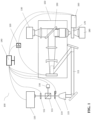
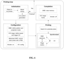
- a line-illumination temporal focusing three-dimensional (3D) nano-fabrication apparatus comprising: a laser source configured to emit a laser beam; a line-illumination pattern unit configured form a pre-determined line pattern from a line-shaped beam; a data acquisition unit configurable to receive input and transmit output signals for movement synchronization of multiple devices; an optical imaging device configured to monitor fabrication process in real time; a controller unit; and a substrate plane.
- the above objectives can be achieved the following a method of three-dimensional (3D) nano-fabricating using a line-illumination temporal focusing 3D nano-fabrication apparatus, the method comprising: (a) generating a series of line patterns from a 3D model; (b) configuring the 3D nano-fabrication apparatus by loading the generated series of line patterns into a memory of a dispersion device in the apparatus; (c) moving a substrate plane that is attached to a sample stage at the focal plane of an obj ective lens; (d) initiating fabrication process by a controller unit wherein a laser beam is emitted from a laser source, passing through an open shutter into a line-illumination unit while the sample stage and a dispersion device moves in synchronization of which is synchronized by a data acquisition unit and continuously move in synchronization in a parallel motion; and (e) completing the fabrication process and once completed, the sample stage returns to its original position, memory of the dispersion device (220) is cleared and
- the present invention teaches a line-illumination temporal focusing three-dimensional (3D) nano-fabrication apparatus 100, the apparatus comprising: a laser source 110 emitting a laser beam 111; a line-illumination pattern unit 150 forming a pre-determined line pattern from a line-shaped beam; a data acquisition unit 120) receiving input and transmitting output signals for movement synchronization of multiple devices; an optical imaging device 130 configured to monitor fabrication process in real time; a controller unit 140; and a substrate plane 170.
- An overall view of the present invention is further illustrated in FIG. 1 .
- the multiple devices synchronized by the acquisition unit 120 are a sample stage 160 and the dispersion device 220 in the line-illumination pattern unit 150, wherein, the acquisition unit 120 receives input signals from the sample stage 160 and transmits output signals to the dispersion device 220 in the line-illumination pattern unit 150 for movement synchronization during fabrication process.
- an illumination light 180 is placed below a sample on the substrate plane 170 wherein an LED light is an example of the illumination light.
- the illumination light 180 is further reconfigurable to be epi-illuminated for an opaque or less transparent object. Other types of illumination lights may be applied, depending on the transparency of the object to be printed.
- the optical imaging device 130 is a 2D imaging sensor selected from a group of complementary metal-oxide-semiconductor CMOS camera and a CCD camera.
- CMOS camera may be employed to monitor the fabrication process in situ, is built in conjunction with the fabrication system and placed at the conjugate plane of the objective lens's focal plane.
- the laser source 110 is a femtosecond fs laser.
- the fs laser has a workable center wavelength ranging from 400 nm - 2000 nm with a wide range of repetition rate i.e., 1kHz - 200 MHz, e.g. 800 nm with a repetition rate of 80 MHz, and a pulse width of ⁇ 150 fs is used as the light source.
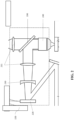
- the line-illumination pattern unit 150 further comprises : a dispersion device 220 with a pre-determined intensity; a shaping lens 230 arranged in adjacent to the dispersion device 220, forming a line-shaped beam; and, a 4-f imaging system to relay the line-shaped beam and focus the laser beam onto a focal plane of an objective lens 240, forming the pre-determined line pattern on the substrate plane 170. More particularly, the laser beam is spatially focused on a Y-Z plane and temporally focused on an X-Z plane of the focal plane of the objective lens which together generates a 3D resolved intensity-programmable line. A close-up view of this embodiment is further illustrated in FIG. 2 .
- the shaping lens 230 is a cylindrical lens
- the 4-f imaging further comprises at least one collimator 211 and the objective lens 240.
- the sample stage 160 is configured to move in X-Y-Z directions and is programmable by the control unit 140 to output trigger signals for the data acquisition unit 120 for movement synchronization during fabrication.
- the data acquisition unit 120 may input trigger signals from the sample stage 160 and output switching signals to the dispersion device 220 for pattern switching.
- the data acquisition unit may also reprogrammable to input signals for arbitrary line structures.
- the controller unit 140 is a computer wherein the computer is configured to control laser source's power, shutter 114, the dispersion device's trigger mode, samples loading into the dispersion's memory, motion and trigger of the sample stage 160.
- the laser beam 111 may expand via a 2 ⁇ - 20 ⁇ beam expander 115 to fill aperture of the dispersion device 220.
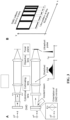
- the dispersion device 220 may be an array of micromirrors or digital micromirror device (DMD) wherein the beam is illuminated onto the DMD chip on the x-z plane and this is illustrated in the upper image of FIG. 3A .
- DMD digital micromirror device
- FIG. 1 Another aspect of the present invention wherein the present invention also teaches a method 300 of three-dimensional 3D nano-fabricating using a line-illumination temporal focusing 3D nano-fabrication apparatus 100, the method comprising: (a) generating a series of line patterns from a 3D model; (b) configuring the 3D nano-fabrication apparatus 100 by loading the generated series of line patterns into a memory of a dispersion device 220 in the apparatus 100; (c) moving a substrate plane 170 that is attached to a sample stage 160 at the focal plane of an objective lens 240; (d) initiating fabrication process by a controller unit 140 wherein a laser beam 111 is emitted from a laser source 110, passing through an open shutter 114 into a line-illumination unit 150 while the sample stage 160 and a dispersion device 220 moves in synchronization of which is synchronized by a data acquisition unit 120 and continuously move in synchronization in a parallel motion; and (e) completing the fabrication process and once completed
- repeating steps (a) to (d) may be required in order to continue fabrication process until all structures are fabricated and once completed, the sample stage 160 returns to its original position, memory of the dispersion device is cleared and the shutter 140 is off.
- adjusting line intensity of the sample in the dispersion device 220 and the sample stage 160 velocity could control laser illumination dose.
- the dispersion device 220 is an array of micromirrors or digital micromirror device (DMD) wherein each line pattern generated from step a further comprising any number of line segments having different grayscale intensities and lengths of which the number and length of the line segments is determined by the number and width of the vertical stripes on the DMD. The intensity of corresponding line segment is determined by the length of the vertical stripes on the DMD.
- DMD digital micromirror device
- step (d) wherein the laser beam 111 emitted from step (d) is reflected by a plurality of reflective mirrors then disperses via the DMD, then enters the concave cylindrical lens 230 and the at least one collimator 211, then is further reflected by a dichroic mirror 190, and lastly enters the objective lens 240 to be spatially and temporally focused into the pre-determined line pattern.
- the data acquisition unit 120 allows movement synchronization of multiple devices.
- the data acquisition unit 120 receives input trigger signals from the sample stage 160 and transmit output switching signals to the DMD for pattern switching.
- the size of the DMD chip is 20.74 mm ⁇ 11.67 mm, which corresponds to a focal line length ( L line ) of 518.5 ⁇ m.
- the stage motion artifacts need to be considered, which may reduce the fabrication rate slightly.
- the DMD (V-9501) has a pattern rate of 18 kHz.
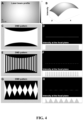
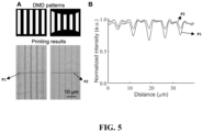
- Light from a fs laser source has a Gaussian profile; and to achieve optimal fabrication results, the laser beam needs to be shaped into a flattop profile, which can be challenging and often results in a complex setup. Yet, this can be easily achieved in the present invention, i.e., by changing patterns displayed on the DMD (or length of each vertical strips in FIG. 3B ), the intensity at each position on the line pattern can be precisely controlled, as illustrated in FIGS.4A-B .
- FIGS. 4G and 4H respectively, present the designed intensity pre-compensated 2D DMD patterns and the simulated illumination line pattern, where precisely controlled gray scale illumination can be clearly observed in the sawtooth profile in the bottom of FIG. 4H .
- the precision of the grayscale control is on the level of 0.1%, which is determined by the number of pixels in the y-axis of the DMD.
- FIGS. 5A-B present the fabrication results of system without and with intensity pre-compensation.
- the light source has a Gaussian beam profile. From FIG. 5B , one may observe clearly that uniformity of the fabricated strips have been significantly improved. The results were fabricated at a rate of 100 mm 3 /hr.
- the present invention invention shows immense market potential in large-scale 3D nanofabrication, which has a broad range of applications in photonics, material design, biomedicine, and semiconductor. It will benefit both the scientific and industrial communities by providing a more capable 3D nano-printing platform in terms of speed, rate, cost, and flexibility. With over 3 orders of magnitude enhancement in the printing speed, this invention can reduce the cost for nanofabrication substantially. It also provides a robust and facile exposure strategy that can be used in different application scenarios, e.g., grayscale printing for tuning the refractive index of photonic devices. Uniform and large-scale complex 3D structures can be fabricated at scale, which promises the rapid prototyping and mass production of functional 3D nanostructures and devices, e.g., mechanical metamaterials and reconfigurable architectures.
Landscapes
- Engineering & Computer Science (AREA)
- Physics & Mathematics (AREA)
- Optics & Photonics (AREA)
- Chemical & Material Sciences (AREA)
- Materials Engineering (AREA)
- Manufacturing & Machinery (AREA)
- Mechanical Engineering (AREA)
- Plasma & Fusion (AREA)
- Health & Medical Sciences (AREA)
- Toxicology (AREA)
- General Physics & Mathematics (AREA)
- Automation & Control Theory (AREA)
- General Health & Medical Sciences (AREA)
- Analytical Chemistry (AREA)
- Microelectronics & Electronic Packaging (AREA)
- Environmental & Geological Engineering (AREA)
- Epidemiology (AREA)
- Public Health (AREA)
- Exposure And Positioning Against Photoresist Photosensitive Materials (AREA)
Applications Claiming Priority (1)
| Application Number | Priority Date | Filing Date | Title |
|---|---|---|---|
| US18/467,170 US20250091156A1 (en) | 2023-09-14 | 2023-09-14 | Line-illumination temporal focusing 3d nano-fabrication apparatus and method |
Publications (1)
| Publication Number | Publication Date |
|---|---|
| EP4523832A1 true EP4523832A1 (de) | 2025-03-19 |
Family
ID=89619994
Family Applications (1)
| Application Number | Title | Priority Date | Filing Date |
|---|---|---|---|
| EP24151859.6A Pending EP4523832A1 (de) | 2023-09-14 | 2024-01-15 | Vorrichtung und verfahren zur herstellung von 3d-nanostrukturen mit zeitlicher linienbeleuchtung |
Country Status (4)
| Country | Link |
|---|---|
| US (1) | US20250091156A1 (de) |
| EP (1) | EP4523832A1 (de) |
| CN (1) | CN119620420A (de) |
| WO (1) | WO2025055143A1 (de) |
Citations (7)
| Publication number | Priority date | Publication date | Assignee | Title |
|---|---|---|---|---|
| US7902526B2 (en) | 2008-04-28 | 2011-03-08 | Massachusetts Institute Of Technology | 3D two-photon lithographic microfabrication system |
| US20160243649A1 (en) * | 2014-07-10 | 2016-08-25 | Guangzhou Institute of Advanced Technology, Chinise Academy of Sciences | Optical system for 3d printing and control method thereof |
| WO2018165613A1 (en) * | 2017-03-10 | 2018-09-13 | Prellis Biologics, Inc. | Methods and systems for printing biological material |
| US10207365B2 (en) | 2015-01-12 | 2019-02-19 | The Chinese University Of Hong Kong | Parallel laser manufacturing system and method |
| WO2020028431A1 (en) * | 2018-07-31 | 2020-02-06 | Prellis Biologics, Inc. | Methods and systems for three-dimensional printing |
| US20210354243A1 (en) | 2014-11-14 | 2021-11-18 | Nikon Corporation | Shaping apparatus and shaping method |
| US11312067B2 (en) | 2017-10-31 | 2022-04-26 | Lawrence Livermore National Security, Llc | System and method for sub micron additive manufacturing |
Family Cites Families (7)
| Publication number | Priority date | Publication date | Assignee | Title |
|---|---|---|---|---|
| CN105954832B (zh) * | 2016-07-14 | 2019-04-16 | 宁波大学 | 一种硫系光纤光栅的无掩模制备装置及方法 |
| US11085018B2 (en) * | 2017-03-10 | 2021-08-10 | Prellis Biologics, Inc. | Three-dimensional printed organs, devices, and matrices |
| JP2020524483A (ja) * | 2017-05-25 | 2020-08-20 | プレリス バイオロジクス,インク. | 三次元印刷された器官、デバイス、およびマトリックス |
| CN111526979B (zh) * | 2017-12-29 | 2023-08-29 | 劳伦斯·利弗莫尔国家安全有限责任公司 | 用于亚微米增材制造的系统和方法 |
| KR20210107653A (ko) * | 2018-11-13 | 2021-09-01 | 프렐리스 바이오로직스, 인크. | 생물학적 물질에 상응하는 3차원 구조체를 프린팅하기 위한 조성물 및 방법 |
| CN115052738B (zh) * | 2019-09-27 | 2025-03-18 | 普瑞利思生物制品公司 | 三维打印器官、设备和基质 |
| CN113834515B (zh) * | 2021-08-18 | 2024-04-16 | 之江实验室 | 一种高时空分辨双光子激光直写原位红外探测装置与方法 |
-
2023
- 2023-09-14 US US18/467,170 patent/US20250091156A1/en active Pending
- 2023-12-04 WO PCT/CN2023/136025 patent/WO2025055143A1/en active Pending
-
2024
- 2024-01-15 EP EP24151859.6A patent/EP4523832A1/de active Pending
- 2024-03-18 CN CN202410304431.0A patent/CN119620420A/zh active Pending
Patent Citations (7)
| Publication number | Priority date | Publication date | Assignee | Title |
|---|---|---|---|---|
| US7902526B2 (en) | 2008-04-28 | 2011-03-08 | Massachusetts Institute Of Technology | 3D two-photon lithographic microfabrication system |
| US20160243649A1 (en) * | 2014-07-10 | 2016-08-25 | Guangzhou Institute of Advanced Technology, Chinise Academy of Sciences | Optical system for 3d printing and control method thereof |
| US20210354243A1 (en) | 2014-11-14 | 2021-11-18 | Nikon Corporation | Shaping apparatus and shaping method |
| US10207365B2 (en) | 2015-01-12 | 2019-02-19 | The Chinese University Of Hong Kong | Parallel laser manufacturing system and method |
| WO2018165613A1 (en) * | 2017-03-10 | 2018-09-13 | Prellis Biologics, Inc. | Methods and systems for printing biological material |
| US11312067B2 (en) | 2017-10-31 | 2022-04-26 | Lawrence Livermore National Security, Llc | System and method for sub micron additive manufacturing |
| WO2020028431A1 (en) * | 2018-07-31 | 2020-02-06 | Prellis Biologics, Inc. | Methods and systems for three-dimensional printing |
Also Published As
| Publication number | Publication date |
|---|---|
| CN119620420A (zh) | 2025-03-14 |
| US20250091156A1 (en) | 2025-03-20 |
| WO2025055143A1 (en) | 2025-03-20 |
Similar Documents
| Publication | Publication Date | Title |
|---|---|---|
| EP3704545B1 (de) | System und verfahren zur tiefenaufgelösten parallelen zwei-photonen-polymerisation für skalierbare generative submikronfertigung | |
| US7088432B2 (en) | Dynamic mask projection stereo micro lithography | |
| US12208569B2 (en) | System and method for submicron additive manufacturing | |
| CN104155851B (zh) | 一种飞秒激光双光子聚合微纳加工系统及方法 | |
| JP4011042B2 (ja) | 光空間変調器、放射線ビームを空間変調する方法、リソグラフィ装置およびデバイス製造方法 | |
| JP7345769B2 (ja) | 直接描画露光システム及び直接描画露光方法 | |
| US10821671B2 (en) | Ultrafast laser fabrication method and system | |
| US20230194992A1 (en) | System and method to control defects in projection-based sub-micrometer additive manufacturing | |
| US12128610B2 (en) | Systems, devices, and methods for kaleidoscopic 3D printing | |
| JP2024533571A (ja) | 3次元コンポーネントのリソグラフィ・ベースの生成的製造のための方法及び装置 | |
| TW201826031A (zh) | 多光子吸收微影加工系統 | |
| KR100709372B1 (ko) | 리소그래피 빔 생성을 위한 방법 및 시스템 | |
| EP4523832A1 (de) | Vorrichtung und verfahren zur herstellung von 3d-nanostrukturen mit zeitlicher linienbeleuchtung | |
| Erdmann et al. | MEMS-based lithography for the fabrication of micro-optical components | |
| EP4257340A1 (de) | Verfahren und vorrichtung zur hochauflösenden schnellen schichtweisen 3d-druckung | |
| US11433602B2 (en) | Stereolithography machine with improved optical group | |
| JP2005260232A (ja) | リソグラフィ装置およびデバイス製造方法 | |
| CN114918532B (zh) | 一种快速扫描式纳米级三维激光加工装置及方法 | |
| US20250144873A1 (en) | System and method for submicron additive manufacturing | |
| EP4523886A1 (de) | 3d-druckvorrichtung mit kombination von digitaler lichtprojektion und zweiphotonenpolymerisation | |
| Zhong et al. | Full-bandwidth, continuous, and grayscale 3D nanolithography via line-illumination temporal focusing of ultrafast lasers | |
| WO2024161177A1 (en) | Method and system for elongating voxel in multiphoton fabrication | |
| GB2639172A (en) | Line-illumination temporal focusing 3D nano-fabrication apparatus and method | |
| KR102005632B1 (ko) | 파면 제어기를 이용한 고속 3차원 광조형 방법 및 장치 | |
| Zhang et al. | Femtosecond 3D Light Field Projection and the Associate 3D Photolithography |
Legal Events
| Date | Code | Title | Description |
|---|---|---|---|
| PUAI | Public reference made under article 153(3) epc to a published international application that has entered the european phase |
Free format text: ORIGINAL CODE: 0009012 |
|
| STAA | Information on the status of an ep patent application or granted ep patent |
Free format text: STATUS: THE APPLICATION HAS BEEN PUBLISHED |
|
| AK | Designated contracting states |
Kind code of ref document: A1 Designated state(s): AL AT BE BG CH CY CZ DE DK EE ES FI FR GB GR HR HU IE IS IT LI LT LU LV MC ME MK MT NL NO PL PT RO RS SE SI SK SM TR |
|
| STAA | Information on the status of an ep patent application or granted ep patent |
Free format text: STATUS: REQUEST FOR EXAMINATION WAS MADE |
|
| 17P | Request for examination filed |
Effective date: 20250919 |