EP4521890A1 - Display device and repair method - Google Patents
Display device and repair method Download PDFInfo
- Publication number
- EP4521890A1 EP4521890A1 EP24195245.6A EP24195245A EP4521890A1 EP 4521890 A1 EP4521890 A1 EP 4521890A1 EP 24195245 A EP24195245 A EP 24195245A EP 4521890 A1 EP4521890 A1 EP 4521890A1
- Authority
- EP
- European Patent Office
- Prior art keywords
- substrate
- transparent
- light
- led
- repair
- Prior art date
- Legal status (The legal status is an assumption and is not a legal conclusion. Google has not performed a legal analysis and makes no representation as to the accuracy of the status listed.)
- Granted
Links
Images


Classifications
-
- H—ELECTRICITY
- H10—SEMICONDUCTOR DEVICES; ELECTRIC SOLID-STATE DEVICES NOT OTHERWISE PROVIDED FOR
- H10H—INORGANIC LIGHT-EMITTING SEMICONDUCTOR DEVICES HAVING POTENTIAL BARRIERS
- H10H29/00—Integrated devices, or assemblies of multiple devices, comprising at least one light-emitting semiconductor element covered by group H10H20/00
- H10H29/80—Constructional details
- H10H29/962—Stacked configurations of light-emitting semiconductor components or devices, the components or devices emitting at different wavelengths
-
- G—PHYSICS
- G09—EDUCATION; CRYPTOGRAPHY; DISPLAY; ADVERTISING; SEALS
- G09G—ARRANGEMENTS OR CIRCUITS FOR CONTROL OF INDICATING DEVICES USING STATIC MEANS TO PRESENT VARIABLE INFORMATION
- G09G3/00—Control arrangements or circuits, of interest only in connection with visual indicators other than cathode-ray tubes
- G09G3/20—Control arrangements or circuits, of interest only in connection with visual indicators other than cathode-ray tubes for presentation of an assembly of a number of characters, e.g. a page, by composing the assembly by combination of individual elements arranged in a matrix no fixed position being assigned to or needed to be assigned to the individual characters or partial characters
- G09G3/22—Control arrangements or circuits, of interest only in connection with visual indicators other than cathode-ray tubes for presentation of an assembly of a number of characters, e.g. a page, by composing the assembly by combination of individual elements arranged in a matrix no fixed position being assigned to or needed to be assigned to the individual characters or partial characters using controlled light sources
- G09G3/30—Control arrangements or circuits, of interest only in connection with visual indicators other than cathode-ray tubes for presentation of an assembly of a number of characters, e.g. a page, by composing the assembly by combination of individual elements arranged in a matrix no fixed position being assigned to or needed to be assigned to the individual characters or partial characters using controlled light sources using electroluminescent panels
- G09G3/32—Control arrangements or circuits, of interest only in connection with visual indicators other than cathode-ray tubes for presentation of an assembly of a number of characters, e.g. a page, by composing the assembly by combination of individual elements arranged in a matrix no fixed position being assigned to or needed to be assigned to the individual characters or partial characters using controlled light sources using electroluminescent panels semiconductive, e.g. using light-emitting diodes [LED]
-
- H—ELECTRICITY
- H10—SEMICONDUCTOR DEVICES; ELECTRIC SOLID-STATE DEVICES NOT OTHERWISE PROVIDED FOR
- H10W—GENERIC PACKAGES, INTERCONNECTIONS, CONNECTORS OR OTHER CONSTRUCTIONAL DETAILS OF DEVICES COVERED BY CLASS H10
- H10W90/00—Package configurations
-
- G—PHYSICS
- G09—EDUCATION; CRYPTOGRAPHY; DISPLAY; ADVERTISING; SEALS
- G09F—DISPLAYING; ADVERTISING; SIGNS; LABELS OR NAME-PLATES; SEALS
- G09F9/00—Indicating arrangements for variable information in which the information is built-up on a support by selection or combination of individual elements
- G09F9/30—Indicating arrangements for variable information in which the information is built-up on a support by selection or combination of individual elements in which the desired character or characters are formed by combining individual elements
- G09F9/33—Indicating arrangements for variable information in which the information is built-up on a support by selection or combination of individual elements in which the desired character or characters are formed by combining individual elements being semiconductor devices, e.g. diodes
-
- H—ELECTRICITY
- H10—SEMICONDUCTOR DEVICES; ELECTRIC SOLID-STATE DEVICES NOT OTHERWISE PROVIDED FOR
- H10H—INORGANIC LIGHT-EMITTING SEMICONDUCTOR DEVICES HAVING POTENTIAL BARRIERS
- H10H20/00—Individual inorganic light-emitting semiconductor devices having potential barriers, e.g. light-emitting diodes [LED]
- H10H20/80—Constructional details
- H10H20/85—Packages
- H10H20/857—Interconnections, e.g. lead-frames, bond wires or solder balls
-
- H—ELECTRICITY
- H10—SEMICONDUCTOR DEVICES; ELECTRIC SOLID-STATE DEVICES NOT OTHERWISE PROVIDED FOR
- H10H—INORGANIC LIGHT-EMITTING SEMICONDUCTOR DEVICES HAVING POTENTIAL BARRIERS
- H10H29/00—Integrated devices, or assemblies of multiple devices, comprising at least one light-emitting semiconductor element covered by group H10H20/00
- H10H29/01—Manufacture or treatment
- H10H29/012—Manufacture or treatment of active-matrix LED displays
-
- H—ELECTRICITY
- H10—SEMICONDUCTOR DEVICES; ELECTRIC SOLID-STATE DEVICES NOT OTHERWISE PROVIDED FOR
- H10H—INORGANIC LIGHT-EMITTING SEMICONDUCTOR DEVICES HAVING POTENTIAL BARRIERS
- H10H29/00—Integrated devices, or assemblies of multiple devices, comprising at least one light-emitting semiconductor element covered by group H10H20/00
- H10H29/30—Active-matrix LED displays
- H10H29/32—Active-matrix LED displays characterised by the geometry or arrangement of elements within a subpixel, e.g. arrangement of the transistor within its RGB subpixel
-
- H—ELECTRICITY
- H10—SEMICONDUCTOR DEVICES; ELECTRIC SOLID-STATE DEVICES NOT OTHERWISE PROVIDED FOR
- H10H—INORGANIC LIGHT-EMITTING SEMICONDUCTOR DEVICES HAVING POTENTIAL BARRIERS
- H10H29/00—Integrated devices, or assemblies of multiple devices, comprising at least one light-emitting semiconductor element covered by group H10H20/00
- H10H29/30—Active-matrix LED displays
- H10H29/45—Active-matrix LED displays comprising two substrates, each having active devices thereon, e.g. displays comprising LED arrays and driving circuitry on different substrates
-
- H—ELECTRICITY
- H10—SEMICONDUCTOR DEVICES; ELECTRIC SOLID-STATE DEVICES NOT OTHERWISE PROVIDED FOR
- H10H—INORGANIC LIGHT-EMITTING SEMICONDUCTOR DEVICES HAVING POTENTIAL BARRIERS
- H10H20/00—Individual inorganic light-emitting semiconductor devices having potential barriers, e.g. light-emitting diodes [LED]
- H10H20/01—Manufacture or treatment
- H10H20/036—Manufacture or treatment of packages
- H10H20/0364—Manufacture or treatment of packages of interconnections
Definitions
- the present disclosure relates to a display device in which a plurality of light-emitting elements are formed on a substrate, and in particular, to repair when a defect occurs in a micro light-emitting diode (LED), and to a repair method for repairing a defective light-emitting diode in a display.
- LED micro light-emitting diode
- micro LEDs that can display images directly from light-emitting diodes have been developed.
- the micro LEDs are two-dimensionally arranged to correspond to pixels.
- each of the pixels includes blue, green, and red sub-pixels.
- JP 2021-504752A discloses a passive-driven display LED stack including: a red (R) first LED stack, a green (G) second LED stack, and a blue (B) third LED stack that are vertically stacked; anodes of the light-emitting diodes of the first LED stack to the third LED stack that are connected to common data interconnect; and cathodes of the light-emitting diodes that are connected to scan interconnects 1, 2, and 3, the R, G, and B light-emitting diodes in the same pixel being driven independently of each other.
- R red
- G green
- B blue
- U.S. 11,171,270B discloses an active-driven micro LED including, on a semiconductor layer: a thin-film transistor (TFT) including a gate electrode, a drain electrode, and a source electrode; a planarization layer formed so as to cover the TFT; a first electrode formed on the planarization layer and connected to the source electrode via a via hole in the planarization layer; and an LED formed between the first electrode and a second electrode that is formed above the first electrode.
- TFT thin-film transistor
- JP 2022-140934A discloses a repair method for removing a defective LED chip from a substrate, on which many LED chips are mounted, by transferring the defective LED chip to an adhesive film by heating the detective LED chip with a laser.
- JP 2023-3062A discloses a chip repair method including: providing a transfer carrier holding a replacement chip; aligning a to-be-repaired part of a to-be-repaired substrate and the replacement chip held on the transfer carrier so as to face each other; and transferring the replacement chip to the to-be-repaired substrate.
- An existing micro LED repair method includes: (1) detecting an abnormal position of a defective micro LED on a substrate by inspection; (2) removing the defective micro LED from the substrate; and (3) remounting a micro LED for repair on the substrate.
- the micro LED is heated with a laser. This requires avoidance of damaging an interconnect pattern, and requires delicate work and many steps, resulting in great increase in cost.
- the present disclosure provides a display device and a repair method capable of readily and cost-effectively repairing a defective LED.
- the first substrate and the second substrate have the same configuration.
- the first interconnect formed on the surface of the first substrate has the same configuration as the second interconnect formed on the surface of the second substrate.
- the display device further includes a drive circuit connected to the first interconnect and the second interconnect, and the drive circuit is configured to simultaneously drive a light-emitting element on the first substrate and a light-emitting element on the second substrate.
- a plurality of light-emitting elements are formed on the second substrate at positions thereon that do not overlap with positions of the plurality of light-emitting elements on the first substrate.
- each of the first interconnect and the second interconnect includes a plurality of data lines and a plurality of scan lines
- the first substrate includes a light-emitting element at intersections between the plurality of data lines and the plurality of scan lines
- the second substrate includes a repair light-emitting element at an intersection between a selected data line and a selected scan line.
- the light-emitting element is a micro LED.
- the repair method is a method for repairing a defective LED in a transparent display in which a plurality of micro LEDs are mounted.
- a second transparent substrate is stacked on a first transparent substrate containing the defective LED, and the repair LED is mounted at a position corresponding to the defective LED on the second transparent substrate.
- the repair light-emitting element is arranged on the second substrate that is stacked on the first substrate, removing the defective light-emitting element from the first substrate becomes unnecessary. Accordingly, the repair work can be simplified, the efficiency of the repair work can be improved, and increase in cost can be suppressed.
- the present disclosure relates to a display device including a substrate on which a plurality of light-emitting elements are formed.
- the present disclosure relates to a display device that, when a defect of the light-emitting element is detected, arranges on a stacked substrate, the light-emitting element for repairing the defective light-emitting element.
- the light-emitting element is not particularly limited, but is, for example, a micro LED. It should be noted that the drawings referred to in the following description include exaggerated representations to facilitate understanding of the disclosure and are not intended to represent the shape or scale of the actual product.
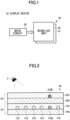
- FIG. 1 is a block diagram illustrating the configuration of a display device according to one embodiment of the present disclosure.
- a display device 10 includes a drive circuit 20 and a transparent display 30 driven by the drive circuit 20.
- the transparent display 30 includes a stack of two micro LED units U1 and U2, and the micro LED units U1 and U2 are driven by the drive circuit 20 independently of each other.
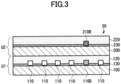
- FIG. 2 is a schematic cross-sectional view of the transparent display 30.
- the lower micro LED unit U1 includes a transparent drive substrate 100, a plurality of micro LEDs 110 arranged in a matrix on the transparent drive substrate 100, and a transparent protective agent 120 formed to cover the surface of the transparent drive substrate 100 including the plurality of micro LEDs 110.
- the upper micro LED unit U2 includes a transparent repair substrate 200, one or a plurality of repair LEDs 210 arranged on the transparent repair substrate 200, and a transparent protective agent 220 formed to cover the surface of the transparent repair substrate 200 including the one or a plurality of repair LEDs 210.
- the transparent repair substrate 200 is stacked on the transparent drive substrate 100 such that a back surface of the transparent repair substrate 200 contacts the transparent protective agent 120.
- the repair LED 210 is mounted on the transparent repair substrate 200 at a position corresponding to the defective LED 110D, i.e., directly above the defective LED 110D.
- the transparent drive substrate 100 and the transparent repair substrate 200 are simultaneously driven, respectively, and the user E sees a composite of an image generated by the transparent drive substrate 100 and an image generated by the transparent repair substrate 200.
- the upper micro LED unit U2 must be formed of a transparent substrate, but the lower micro LED unit U1 may not necessarily be a transparent substrate.
- a transparent display using micro LEDs has several tens of ⁇ m of LED chips, and a full high definition (HD) display has 1920 ⁇ 1080 pixels, and the number of LED chips to be mounted is 1920 ⁇ 1080 ⁇ 3 (RGB), or approximately 6.22 million. Therefore, LED defects often occur, and repair work is essential. Existing repair work requires many man-hours to remove defective LEDs and to transfer the detective LEDs, etc. Also, these processes require delicacy that does not damage the interconnect pattern on the substrate, thus, resulting in an increase in cost. On the other hand, as in the present embodiment, it is more advantageous in terms of process simplification and costs, to stack a transparent repair substrate and mount the LEDs for repair on the transparent repair substrate.
- FIG. 3 is a schematic cross-sectional view of a transparent display of a display device according to the first embodiment of the present disclosure, and the same reference numerals as those of FIG. 2 are used for the same configuration.
- the lower micro LED unit U1 includes a rectangular transparent drive substrate 100.
- the transparent drive substrate 100 is configured using, for example, a light-transmissive substrate such as glass, plastic, acrylic, or a transparent film.
- a substrate interconnect 130 is formed on the surface of the transparent drive substrate 100.
- the material of the substrate interconnect 130 is not particularly limited, but is, for example, a conductive material such as Cu or a light-transmissive conductive material such as ITO. Using these conductive materials, an interconnect pattern (for example, data electrode interconnect, scan electrode interconnect, etc.) is formed on the transparent drive substrate 100.
- the plurality of micro LEDs 110 are mounted in a matrix or arbitrary pattern (for example, 8-segment display) on the surface of the transparent drive substrate 100 so as to be electrically connected to the substrate interconnect 130. For example, at each intersection of the data electrode interconnect and the scan electrode interconnect, one electrode of the micro LED is connected to the data electrode interconnect, and the other electrode is connected to the scan electrode interconnect.
- a matrix or arbitrary pattern for example, 8-segment display
- a transparent protective agent 120 is formed on the transparent drive substrate 100 to cover the plurality of micro LEDs 110.
- the transparent protective agent 120 is formed of materials such as, but not limited to, polyethylene terephthalate (PET), polypropylene (PP), and polyvinyl chloride (PVC).
- the upper micro LED unit U2 includes a transparent repair substrate 200 on which a substrate interconnect 230 is formed.
- the transparent repair substrate 200 includes the same material, has the same size, and includes the same substrate interconnect as the transparent drive substrate 100. Accordingly, the transparent drive substrate 100 and the transparent repair substrate 200 have a same configuration.
- the transparent repair substrate 200 may be made of a different material, have a different size, and include different substrate interconnect from the transparent drive substrate 200.
- the former embodiment is more cost advantageous because the transparent substrates have the same configuration.
- a repair LED 210 is mounted on the transparent repair substrate 200 at a position corresponding to a defective LED on the transparent drive substrate 100.
- the repair LED 210 is mounted on the transparent repair substrate 200 by, for example, thermal pressure bonding a material containing conductive particles on the substrate interconnect 230.
- a transparent protective agent 220 is formed on the transparent repair substrate 200 to cover one or a plurality of repair LEDs 210.
- FIG. 4A is a schematic plan view of a transparent drive substrate
- FIG. 4B is a schematic plan view of a transparent repair substrate.
- a plurality of scan electrode interconnects S1, S2, ..., S5, and S6 extending in a row direction (X direction) and a plurality of data electrode interconnects D1, D2, ..., D5, and D6 extending in a column direction (Y direction) are formed on the transparent drive substrate 100 as substrate interconnects 130.
- a micro LED 110 is connected to each intersection of the plurality of scan electrode interconnects and the plurality of data electrode interconnects.
- a switching element may be arranged at the intersections of the scan electrode interconnects and the data electrode interconnects to serve as active driving.
- the scan electrode interconnects and the data electrode interconnects are illustrated linearly, the shape and pattern of the interconnects are appropriately determined according to the position of the anode/cathode of the micro LED.
- the cathode electrode of the micro LED is electrically connected to the scan electrode interconnect
- the anode electrode of the micro LED is electrically connected to the data electrode interconnect.
- one pixel is illustrated as one micro LED.
- one pixel is formed of three sub-pixels that generate red (R), green (G), and blue (B).
- the composition of the R, G, and B sub-pixels is not particularly limited, but may be formed of, for example, a red-emitting diode, a green-emitting diode, and a blue-emitting diode, or alternatively, a fluorescent filter that generates red and green from the blue-emitting diode may be used to form the R and G light-emitting elements.
- each of the R, G, and B sub-pixels is connected to both the scan electrode interconnect and the data electrode interconnect.
- the micro LED may be, for example, a white diode generating white light or an infrared diode generating infrared light.
- two defective LEDs 110D are illustrated at the intersection of the scan electrode interconnect S5 and the data electrode interconnect D6 and the intersection of the scan electrode interconnect S6 and the data electrode interconnect D4.
- the defective LED 110D represents a defect in one of the R, G, and B sub-pixels.
- a defect in the LED includes, for example, a defective connection between the anode/cathode electrodes of the micro LED and the interconnect, or a failure or defect of the LED itself.
- detection of the defective LED causes all of the micro LEDs 110 mounted on the transparent drive substrate 100 to be fully lit, and at this time identifies the location of the micro LEDs not emitting light.
- an imaging camera may be used to image the fully light-emitting micro LEDs of the transparent drive substrate 100, detect the location of the micro LEDs not emitting light from the captured image, and determine the micro LEDs not emitting light to be the defective LEDs.
- the defective LED detection processing may be performed using, for example, a computer device, and the positional information of the defective LEDs may be used when mounting the repair LEDs 210 on the transparent repair substrate 200.
- the scan electrode interconnect and the data electrode interconnect as illustrated in FIG. 4A are interconnects for passive driving.
- the drive circuit 20 as illustrated in FIG. 1 drives the scan electrode interconnect by time-division at a constant scan frequency. Also, the drive circuit 20 applies, in synchronization with the scan frequency of the scan electrode interconnect, a data signal (drive current) corresponding to the image data to be displayed to the data electrode interconnects D1, D2, ..., D5, and D6. As a result, the micro LED emits light at a luminance corresponding to the applied data signal.
- the scan electrode interconnect S1 when the scan electrode interconnect S1 is driven, data signals from the data electrode interconnects D1, D2, ..., D5, and D6 are applied to respective micro LEDs at the intersections of the scan electrode interconnect S1 and the data electrode interconnects D1, D2, ..., D5, and D6, and the micro LEDs of this line emit light.
- the scan electrode interconnect S2 when the scan electrode interconnect S2 is driven, data signals from the data electrode interconnects D1, D2, ..., D5, and D6 are applied to respective micro LEDs at the intersections of the scan electrode interconnect S2, and the micro LEDs of this line emit light.
- the scan electrode interconnects are sequentially driven from S1 to S6 to display one frame.
- the defective LED 110D at the intersection of the scan electrode interconnect S5 and the data electrode interconnect D6, and the defective LED 110D at the intersection of the scan electrode interconnect S6 and the data electrode interconnect D4 do not emit light.
- the transparent repair substrate 200 includes the same substrate interconnect as the transparent drive substrate 100, that is, the same scan electrode interconnect and data electrode interconnect. However, only the repair LED 210 for compensating the defective LED 110D is mounted on the transparent repair substrate 200. For example, when the defective LED is a subpixel R micro LED, the repair LED is an R micro LED. When the transparent repair substrate 200 is aligned with the transparent drive substrate 100, the repair LED 210 is arranged at a position corresponding to the defective LED 110D.
- the drive circuit 20 is connected to the micro LED units U1 and U2, respectively, and drives the micro LED units U1 and U2 simultaneously with and independently of each other. That is, the scan electrode interconnect and the data electrode interconnect that are of the transparent drive substrate 100 and the transparent repair substrate 200 are simultaneously driven. For example, when the scan electrode interconnect S5 is scanned, the defective LED 110D of the data electrode interconnect D6 of the transparent drive substrate 100 does not emit light, but the repair LED 210R of the transparent repair substrate 200 emits light in response to the data signal applied from the data electrode interconnect D6.
- the defective LED 110D of the data electrode interconnect D4 of the transparent drive substrate 100 does not emit light, but the repair LED 210R of the transparent repair substrate 200 emits light in response to the data signal applied from the data electrode interconnect D4.
- the transparent drive substrate and the transparent repair substrate having the same configuration, it is possible to repair only with the existing transparent drive substrate without generating a new transparent repair substrate, and as a result, the cost of the display device can be reduced.
- FIG. 5 is a schematic cross-sectional view of a transparent display according to the second embodiment.
- the substrate interconnect 130 of the transparent drive substrate 100 and the substrate interconnect 230 of the transparent repair substrate 200 that are used in the first embodiment are connected by the interconnect 240, and the connected interconnect 240 is connected to the drive circuit 20.
- the drive circuit 20 drives the transparent drive substrate 100 and the transparent repair substrate 200 through the common interconnect 240.
- a dedicated drive circuit for the transparent repair substrate 200 is not required, thereby reducing the cost. Since the transparent drive substrate 100 and the transparent repair substrate 200 are interconnect boards of same configuration, they can be easily connected by using an inter-board connector for interconnect connection.
- a repair LED is mounted on an upper transparent drive substrate using a method of stacking a transparent drive substrate on which a micro LED is mounted.
- FIG. 6A is a schematic cross-sectional view of the transparent display 30A according to the third embodiment.
- the transparent display 30A includes a stack of a lower micro LED unit U1 and an upper micro LED unit U2.
- the lower micro LED unit U1 includes a lower transparent drive substrate 300, a plurality of micro LEDs 310 two-dimensionally mounted on the lower transparent drive substrate 300, and a transparent protective agent 320 covering the surface of the lower transparent drive substrate 300.
- the upper micro LED unit U2 includes an upper transparent drive substrate 400, a plurality of micro LEDs 410 two-dimensionally mounted on the upper transparent drive substrate 400, and a transparent protective agent 420 covering the surface of the upper transparent drive substrate 400.
- the micro LEDs 310 mounted on the lower transparent drive substrate 300 are arranged such that positions thereon do not overlap with those of the micro LEDs 420 mounted on the upper transparent drive substrate 400.
- the rows and columns of the micro LEDs 310 are shifted by 1/2 from the rows and columns of the micro LEDs 420 so that the micro LEDs 310 and micro LEDs 420 are arranged in a staggered manner.
- Light emitted from the micro LED 310 of the lower transparent drive substrate 300 enters from the back surface of the upper transparent drive substrate 400 and is emitted from the front surface of the transparent protective agent 420.
- light emitted from the micro LED 410 of the upper transparent drive substrate 400 is also emitted through the transparent protective agent 420 from the front surface thereof.
- a frame image generated by the micro LED unit U1 and a frame image generated by the micro LED unit U2 are combined to display a high-resolution and high-definition image.
- a repair LED 410R is mounted to the position corresponding to the defective LED 310D on the upper transparent drive substrate 400.
- the repair LED when a high-definition transparent display is configured by stacking the transparent drive substrates, the repair LED can be arranged on the upper transparent drive substrate. Accordingly, by not adding a new repair substrate, a more cost-advantageous configuration can be achieved as described in the first and second embodiments.
Landscapes
- Engineering & Computer Science (AREA)
- Physics & Mathematics (AREA)
- General Physics & Mathematics (AREA)
- Theoretical Computer Science (AREA)
- Devices For Indicating Variable Information By Combining Individual Elements (AREA)
- Computer Hardware Design (AREA)
- Led Device Packages (AREA)
Abstract
Description
- The present disclosure relates to a display device in which a plurality of light-emitting elements are formed on a substrate, and in particular, to repair when a defect occurs in a micro light-emitting diode (LED), and to a repair method for repairing a defective light-emitting diode in a display.
- In recent years, micro LEDs that can display images directly from light-emitting diodes have been developed. The micro LEDs are two-dimensionally arranged to correspond to pixels. For color images, each of the pixels includes blue, green, and red sub-pixels.
- For example,
JP 2021-504752A scan interconnects -
U.S. 11,171,270B - In a display using a micro LED, when a failure or a defect of mounting of the micro LED occurs, it is necessary to repair the micro LED. For example,
JP 2022-140934A JP 2023-3062A - An existing micro LED repair method includes: (1) detecting an abnormal position of a defective micro LED on a substrate by inspection; (2) removing the defective micro LED from the substrate; and (3) remounting a micro LED for repair on the substrate. However, for removal of the micro LED, the micro LED is heated with a laser. This requires avoidance of damaging an interconnect pattern, and requires delicate work and many steps, resulting in great increase in cost.
- The present disclosure provides a display device and a repair method capable of readily and cost-effectively repairing a defective LED.
- The present disclosure relates to a display device and a repair method according to the appended claims. Embodiments are disclosed in the dependent claims. The display device according to an aspect of the present disclosure includes: a first substrate including a plurality of light-emitting elements arranged two-dimensionally; and a second substrate stacked on the first substrate. At least the second substrate is transparent. The second substrate includes a repair light-emitting element arranged on the second substrate at a position thereon that corresponds to a defective light-emitting element on the first substrate.
- In one embodiment, the first substrate and the second substrate have the same configuration. In a further embodiment, the first interconnect formed on the surface of the first substrate has the same configuration as the second interconnect formed on the surface of the second substrate. In one embodiment, the display device further includes a drive circuit connected to the first interconnect and the second interconnect, and the drive circuit is configured to simultaneously drive a light-emitting element on the first substrate and a light-emitting element on the second substrate. In one embodiment, a plurality of light-emitting elements are formed on the second substrate at positions thereon that do not overlap with positions of the plurality of light-emitting elements on the first substrate. In one embodiment, each of the first interconnect and the second interconnect includes a plurality of data lines and a plurality of scan lines, the first substrate includes a light-emitting element at intersections between the plurality of data lines and the plurality of scan lines, and the second substrate includes a repair light-emitting element at an intersection between a selected data line and a selected scan line. In one embodiment, the light-emitting element is a micro LED.
- The repair method according to a further aspect of the present disclosure is a method for repairing a defective LED in a transparent display in which a plurality of micro LEDs are mounted. In the repair method, a second transparent substrate is stacked on a first transparent substrate containing the defective LED, and the repair LED is mounted at a position corresponding to the defective LED on the second transparent substrate.
- According to aspects of the present disclosure, since the repair light-emitting element is arranged on the second substrate that is stacked on the first substrate, removing the defective light-emitting element from the first substrate becomes unnecessary. Accordingly, the repair work can be simplified, the efficiency of the repair work can be improved, and increase in cost can be suppressed.
-
FIG. 1 is a block diagram illustrating a schematic configuration of a display device according to one embodiment of the present disclosure; -
FIG. 2 is a schematic cross-sectional view of a transparent display according to one embodiment of the present disclosure; -
FIG. 3 is a schematic cross-sectional view of a transparent display of a display device according to a first embodiment of the present disclosure; -
FIG. 4A is a schematic plan view of a transparent drive substrate according to the first embodiment; -
FIG. 4B is a schematic plan view of a transparent repair substrate according to the first embodiment; -
FIG. 5 is a schematic cross-sectional view of a transparent display according to a second embodiment of the present disclosure; -
FIG. 6A is a schematic cross-sectional view of a transparent display according to a third embodiment of the present disclosure; and -
FIG. 6B is a schematic cross-sectional view of the transparent display according to the third embodiment of the present disclosure. - The present disclosure relates to a display device including a substrate on which a plurality of light-emitting elements are formed. In particular, the present disclosure relates to a display device that, when a defect of the light-emitting element is detected, arranges on a stacked substrate, the light-emitting element for repairing the defective light-emitting element. The light-emitting element is not particularly limited, but is, for example, a micro LED. It should be noted that the drawings referred to in the following description include exaggerated representations to facilitate understanding of the disclosure and are not intended to represent the shape or scale of the actual product.
-
FIG. 1 is a block diagram illustrating the configuration of a display device according to one embodiment of the present disclosure. As illustrated inFIG. 1 , adisplay device 10 includes adrive circuit 20 and atransparent display 30 driven by thedrive circuit 20. Thetransparent display 30 includes a stack of two micro LED units U1 and U2, and the micro LED units U1 and U2 are driven by thedrive circuit 20 independently of each other. -
FIG. 2 is a schematic cross-sectional view of thetransparent display 30. The lower micro LED unit U1 includes atransparent drive substrate 100, a plurality ofmicro LEDs 110 arranged in a matrix on thetransparent drive substrate 100, and a transparentprotective agent 120 formed to cover the surface of thetransparent drive substrate 100 including the plurality ofmicro LEDs 110. The upper micro LED unit U2 includes atransparent repair substrate 200, one or a plurality of repair LEDs 210 arranged on thetransparent repair substrate 200, and a transparentprotective agent 220 formed to cover the surface of thetransparent repair substrate 200 including the one or a plurality of repair LEDs 210. Thetransparent repair substrate 200 is stacked on thetransparent drive substrate 100 such that a back surface of thetransparent repair substrate 200 contacts the transparentprotective agent 120. - When a
defective LED 110D is detected among a plurality ofmicro LEDs 110 mounted on thetransparent drive substrate 100, the repair LED 210 is mounted on thetransparent repair substrate 200 at a position corresponding to thedefective LED 110D, i.e., directly above thedefective LED 110D. When the image is displayed by thetransparent display 30, thetransparent drive substrate 100 and thetransparent repair substrate 200 are simultaneously driven, respectively, and the user E sees a composite of an image generated by thetransparent drive substrate 100 and an image generated by thetransparent repair substrate 200. - Thus, by supplementing the
defective LED 110D of thetransparent drive substrate 100 with the LED 210 of the stackedtransparent repair substrate 200, it is possible to eliminate the work of removing thedefective LED 110D from thetransparent drive substrate 100 as in the existing manner. It should be noted that the upper micro LED unit U2 must be formed of a transparent substrate, but the lower micro LED unit U1 may not necessarily be a transparent substrate. - A transparent display using micro LEDs has several tens of µm of LED chips, and a full high definition (HD) display has 1920×1080 pixels, and the number of LED chips to be mounted is 1920×1080×3 (RGB), or approximately 6.22 million. Therefore, LED defects often occur, and repair work is essential. Existing repair work requires many man-hours to remove defective LEDs and to transfer the detective LEDs, etc. Also, these processes require delicacy that does not damage the interconnect pattern on the substrate, thus, resulting in an increase in cost. On the other hand, as in the present embodiment, it is more advantageous in terms of process simplification and costs, to stack a transparent repair substrate and mount the LEDs for repair on the transparent repair substrate.
- Next, a first embodiment of the present disclosure will be described.
FIG. 3 is a schematic cross-sectional view of a transparent display of a display device according to the first embodiment of the present disclosure, and the same reference numerals as those ofFIG. 2 are used for the same configuration. - The lower micro LED unit U1 includes a rectangular
transparent drive substrate 100. Thetransparent drive substrate 100 is configured using, for example, a light-transmissive substrate such as glass, plastic, acrylic, or a transparent film. - A
substrate interconnect 130 is formed on the surface of thetransparent drive substrate 100. The material of thesubstrate interconnect 130 is not particularly limited, but is, for example, a conductive material such as Cu or a light-transmissive conductive material such as ITO. Using these conductive materials, an interconnect pattern (for example, data electrode interconnect, scan electrode interconnect, etc.) is formed on thetransparent drive substrate 100. - The plurality of
micro LEDs 110 are mounted in a matrix or arbitrary pattern (for example, 8-segment display) on the surface of thetransparent drive substrate 100 so as to be electrically connected to thesubstrate interconnect 130. For example, at each intersection of the data electrode interconnect and the scan electrode interconnect, one electrode of the micro LED is connected to the data electrode interconnect, and the other electrode is connected to the scan electrode interconnect. - A transparent
protective agent 120 is formed on thetransparent drive substrate 100 to cover the plurality ofmicro LEDs 110. The transparentprotective agent 120 is formed of materials such as, but not limited to, polyethylene terephthalate (PET), polypropylene (PP), and polyvinyl chloride (PVC). - The upper micro LED unit U2 includes a
transparent repair substrate 200 on which asubstrate interconnect 230 is formed. In one embodiment, thetransparent repair substrate 200 includes the same material, has the same size, and includes the same substrate interconnect as thetransparent drive substrate 100. Accordingly, thetransparent drive substrate 100 and thetransparent repair substrate 200 have a same configuration. In another embodiment, thetransparent repair substrate 200 may be made of a different material, have a different size, and include different substrate interconnect from thetransparent drive substrate 200. However, the former embodiment is more cost advantageous because the transparent substrates have the same configuration. - A repair LED 210 is mounted on the
transparent repair substrate 200 at a position corresponding to a defective LED on thetransparent drive substrate 100. The repair LED 210 is mounted on thetransparent repair substrate 200 by, for example, thermal pressure bonding a material containing conductive particles on thesubstrate interconnect 230. A transparentprotective agent 220 is formed on thetransparent repair substrate 200 to cover one or a plurality of repair LEDs 210. -
FIG. 4A is a schematic plan view of a transparent drive substrate, andFIG. 4B is a schematic plan view of a transparent repair substrate. As illustrated inFIG. 4A , a plurality of scan electrode interconnects S1, S2, ..., S5, and S6 extending in a row direction (X direction) and a plurality of data electrode interconnects D1,
D2, ..., D5, and D6 extending in a column direction (Y direction) are formed on thetransparent drive substrate 100 as substrate interconnects 130. Amicro LED 110 is connected to each intersection of the plurality of scan electrode interconnects and the plurality of data electrode interconnects. Although the six scan electrode interconnects and the data electrode interconnects of passive driving are illustrated here for convenience, the number of scan electrode interconnects and the data electrode interconnects according to the number of pixels are actually formed. A switching element may be arranged at the intersections of the scan electrode interconnects and the data electrode interconnects to serve as active driving. - Although the scan electrode interconnects and the data electrode interconnects are illustrated linearly, the shape and pattern of the interconnects are appropriately determined according to the position of the anode/cathode of the micro LED. At the intersection of the scan electrode interconnect and the data electrode interconnect, for example, the cathode electrode of the micro LED is electrically connected to the scan electrode interconnect, and the anode electrode of the micro LED is electrically connected to the data electrode interconnect.
- In
FIG. 4A , one pixel is illustrated as one micro LED. However, when thetransparent display 30 displays a color image, one pixel is formed of three sub-pixels that generate red (R), green (G), and blue (B). The composition of the R, G, and B sub-pixels is not particularly limited, but may be formed of, for example, a red-emitting diode, a green-emitting diode, and a blue-emitting diode, or alternatively, a fluorescent filter that generates red and green from the blue-emitting diode may be used to form the R and G light-emitting elements. When the R, G, and B sub-pixels are included, each of the R, G, and B sub-pixels is connected to both the scan electrode interconnect and the data electrode interconnect. The micro LED may be, for example, a white diode generating white light or an infrared diode generating infrared light. - In
FIG. 4A , twodefective LEDs 110D are illustrated at the intersection of the scan electrode interconnect S5 and the data electrode interconnect D6 and the intersection of the scan electrode interconnect S6 and the data electrode interconnect D4. When the micro LED includes R, G, and B sub-pixels, thedefective LED 110D represents a defect in one of the R, G, and B sub-pixels. A defect in the LED includes, for example, a defective connection between the anode/cathode electrodes of the micro LED and the interconnect, or a failure or defect of the LED itself. - In one embodiment, detection of the defective LED causes all of the
micro LEDs 110 mounted on thetransparent drive substrate 100 to be fully lit, and at this time identifies the location of the micro LEDs not emitting light. For example, an imaging camera may be used to image the fully light-emitting micro LEDs of thetransparent drive substrate 100, detect the location of the micro LEDs not emitting light from the captured image, and determine the micro LEDs not emitting light to be the defective LEDs. The defective LED detection processing may be performed using, for example, a computer device, and the positional information of the defective LEDs may be used when mounting the repair LEDs 210 on thetransparent repair substrate 200. - The scan electrode interconnect and the data electrode interconnect as illustrated in
FIG. 4A are interconnects for passive driving. Thedrive circuit 20 as illustrated inFIG. 1 drives the scan electrode interconnect by time-division at a constant scan frequency. Also, thedrive circuit 20 applies, in synchronization with the scan frequency of the scan electrode interconnect, a data signal (drive current) corresponding to the image data to be displayed to the data electrode interconnects D1, D2, ..., D5, and D6. As a result, the micro LED emits light at a luminance corresponding to the applied data signal. - For example, when the scan electrode interconnect S1 is driven, data signals from the data electrode interconnects D1, D2, ..., D5, and D6 are applied to respective micro LEDs at the intersections of the scan electrode interconnect S1 and the data electrode interconnects D1, D2, ..., D5, and D6, and the micro LEDs of this line emit light. Next, when the scan electrode interconnect S2 is driven, data signals from the data electrode interconnects D1, D2, ..., D5, and D6 are applied to respective micro LEDs at the intersections of the scan electrode interconnect S2, and the micro LEDs of this line emit light. In such a way, the scan electrode interconnects are sequentially driven from S1 to S6 to display one frame. In the example as illustrated in the figure, the
defective LED 110D at the intersection of the scan electrode interconnect S5 and the data electrode interconnect D6, and thedefective LED 110D at the intersection of the scan electrode interconnect S6 and the data electrode interconnect D4, do not emit light. - As illustrated in
FIG. 4B , thetransparent repair substrate 200 includes the same substrate interconnect as thetransparent drive substrate 100, that is, the same scan electrode interconnect and data electrode interconnect. However, only the repair LED 210 for compensating thedefective LED 110D is mounted on thetransparent repair substrate 200. For example, when the defective LED is a subpixel R micro LED, the repair LED is an R micro LED. When thetransparent repair substrate 200 is aligned with thetransparent drive substrate 100, the repair LED 210 is arranged at a position corresponding to thedefective LED 110D. - The
drive circuit 20 is connected to the micro LED units U1 and U2, respectively, and drives the micro LED units U1 and U2 simultaneously with and independently of each other. That is, the scan electrode interconnect and the data electrode interconnect that are of thetransparent drive substrate 100 and thetransparent repair substrate 200 are simultaneously driven. For example, when the scan electrode interconnect S5 is scanned, thedefective LED 110D of the data electrode interconnect D6 of thetransparent drive substrate 100 does not emit light, but therepair LED 210R of thetransparent repair substrate 200 emits light in response to the data signal applied from the data electrode interconnect D6. Then, when the scan electrode interconnect S6 is scanned, thedefective LED 110D of the data electrode interconnect D4 of thetransparent drive substrate 100 does not emit light, but therepair LED 210R of thetransparent repair substrate 200 emits light in response to the data signal applied from the data electrode interconnect D4. - According to the present embodiment, by the transparent drive substrate and the transparent repair substrate having the same configuration, it is possible to repair only with the existing transparent drive substrate without generating a new transparent repair substrate, and as a result, the cost of the display device can be reduced.
- Next, a second embodiment of the present disclosure will be described.
FIG. 5 is a schematic cross-sectional view of a transparent display according to the second embodiment. In the second embodiment, thesubstrate interconnect 130 of thetransparent drive substrate 100 and thesubstrate interconnect 230 of thetransparent repair substrate 200 that are used in the first embodiment are connected by theinterconnect 240, and theconnected interconnect 240 is connected to thedrive circuit 20. Thedrive circuit 20 drives thetransparent drive substrate 100 and thetransparent repair substrate 200 through thecommon interconnect 240. As a result, a dedicated drive circuit for thetransparent repair substrate 200 is not required, thereby reducing the cost. Since thetransparent drive substrate 100 and thetransparent repair substrate 200 are interconnect boards of same configuration, they can be easily connected by using an inter-board connector for interconnect connection. - Next, a third embodiment of the present disclosure will be described. In the third embodiment, in order to achieve a high-resolution and high-definition transparent display, a repair LED is mounted on an upper transparent drive substrate using a method of stacking a transparent drive substrate on which a micro LED is mounted.
-
FIG. 6A is a schematic cross-sectional view of thetransparent display 30A according to the third embodiment. Thetransparent display 30A includes a stack of a lower micro LED unit U1 and an upper micro LED unit U2. The lower micro LED unit U1 includes a lowertransparent drive substrate 300, a plurality ofmicro LEDs 310 two-dimensionally mounted on the lowertransparent drive substrate 300, and a transparentprotective agent 320 covering the surface of the lowertransparent drive substrate 300. The upper micro LED unit U2 includes an uppertransparent drive substrate 400, a plurality ofmicro LEDs 410 two-dimensionally mounted on the uppertransparent drive substrate 400, and a transparentprotective agent 420 covering the surface of the uppertransparent drive substrate 400. - The
micro LEDs 310 mounted on the lowertransparent drive substrate 300 are arranged such that positions thereon do not overlap with those of themicro LEDs 420 mounted on the uppertransparent drive substrate 400. For example, the rows and columns of themicro LEDs 310 are shifted by 1/2 from the rows and columns of themicro LEDs 420 so that themicro LEDs 310 andmicro LEDs 420 are arranged in a staggered manner. - When an image is displayed on the
transparent display 30A, thedrive circuit 20 drives the micro LED unit U1 by time division at a scan frequency F1 and drives the micro LED unit U2 by time division at a scan frequency F2 (F2 = F1). Light emitted from themicro LED 310 of the lowertransparent drive substrate 300 enters from the back surface of the uppertransparent drive substrate 400 and is emitted from the front surface of the transparentprotective agent 420. Additionally, light emitted from themicro LED 410 of the uppertransparent drive substrate 400 is also emitted through the transparentprotective agent 420 from the front surface thereof. Thus, a frame image generated by the micro LED unit U1 and a frame image generated by the micro LED unit U2 are combined to display a high-resolution and high-definition image. - Here, as illustrated in
FIG. 6B , when adefective LED 310D is detected on the lowertransparent drive substrate 300, arepair LED 410R is mounted to the position corresponding to thedefective LED 310D on the uppertransparent drive substrate 400. - Thus, according to the present embodiment, when a high-definition transparent display is configured by stacking the transparent drive substrates, the repair LED can be arranged on the upper transparent drive substrate. Accordingly, by not adding a new repair substrate, a more cost-advantageous configuration can be achieved as described in the first and second embodiments.
- Although embodiments of the present invention have been described in detail above, the present invention is not limited to these specific embodiments and can be modified in various ways within the scope of the claims.
Claims (8)
- A display device, comprising:a first substrate including a plurality of light-emitting elements arranged two-dimensionally; anda second substrate stacked on the first substrate, whereinat least the second substrate is transparent, andthe second substrate includes a repair light-emitting element arranged on the second substrate at a position thereon that corresponds to a defective light-emitting element on the first substrate, the defective light-emitting element being from among the light-emitting elements.
- The display device according to claim 1, wherein the first substrate and the second substrate have a same configuration.
- The display device according to claim 1 or 2, wherein
a first interconnect formed on a surface of the first substrate has a same configuration as a second interconnect formed on a surface of the second substrate. - The display device according to claim 3, further comprising:
a drive circuit connected to the first interconnect and the second interconnect, wherein
the drive circuit is configured to simultaneously drive the light-emitting elements on the first substrate and a light-emitting element on the second substrate. - The display device according to one of claims 1 to 4, wherein
the second substrate includes a plurality of light-emitting elements formed on the second substrate at positions thereon that do not overlap with positions of the plurality of light-emitting elements on the first substrate. - The display device according to one of claims 3 to 5, whereinthe first interconnect and the second interconnect each include a plurality of data lines and a plurality of scan lines,the first substrate includes the light-emitting elements at intersections between the plurality of data lines and the plurality of scan lines, andthe second substrate includes a repair light-emitting element at an intersection of: a selected data line that is selected from the plurality of data lines; and a selected scan line that is selected from the plurality of scan lines.
- The display device according to one of claims 1 to 6, wherein the light-emitting elements are each a micro light-emitting diode (LED).
- A repair method for repairing a defective light-emitting diode (LED) in a display mounted with a plurality of micro LEDs, the repair method comprising:stacking a second transparent substrate on a first substrate including the defective LED, andmounting a repair LED on the second transparent substrate at a position thereon that corresponds to the defective LED.
Applications Claiming Priority (1)
| Application Number | Priority Date | Filing Date | Title |
|---|---|---|---|
| JP2023145916A JP2025039079A (en) | 2023-09-08 | 2023-09-08 | Display device and repair method |
Publications (2)
| Publication Number | Publication Date |
|---|---|
| EP4521890A1 true EP4521890A1 (en) | 2025-03-12 |
| EP4521890B1 EP4521890B1 (en) | 2026-01-21 |
Family
ID=92458998
Family Applications (1)
| Application Number | Title | Priority Date | Filing Date |
|---|---|---|---|
| EP24195245.6A Active EP4521890B1 (en) | 2023-09-08 | 2024-08-19 | Display device and repair method |
Country Status (4)
| Country | Link |
|---|---|
| US (1) | US20250087649A1 (en) |
| EP (1) | EP4521890B1 (en) |
| JP (1) | JP2025039079A (en) |
| CN (1) | CN119626145A (en) |
Citations (7)
| Publication number | Priority date | Publication date | Assignee | Title |
|---|---|---|---|---|
| US20180151632A1 (en) * | 2016-11-29 | 2018-05-31 | Gwangju Institute Of Science And Technology | Micro display having vertically stacked structure and method of forming the same |
| US20190172760A1 (en) * | 2017-12-05 | 2019-06-06 | Acer Incorporated | Micro lighting device |
| US20200388736A1 (en) * | 2019-06-06 | 2020-12-10 | PlayNitride Display Co., Ltd. | Method for fabricating micro light-emitting diode display |
| JP2021504752A (en) | 2017-11-27 | 2021-02-15 | ソウル バイオシス カンパニー リミテッドSeoul Viosys Co.,Ltd. | LED unit for display and display device having it |
| US11171270B2 (en) | 2016-04-11 | 2021-11-09 | Samsung Display Co., Ltd. | Display apparatus |
| JP2022140934A (en) | 2021-03-15 | 2022-09-29 | 東レエンジニアリング株式会社 | chip remover |
| JP2023003062A (en) | 2021-06-23 | 2023-01-11 | 東レエンジニアリング株式会社 | Chip repair method and chip repair system |
-
2023
- 2023-09-08 JP JP2023145916A patent/JP2025039079A/en active Pending
-
2024
- 2024-07-17 US US18/775,359 patent/US20250087649A1/en active Pending
- 2024-08-19 EP EP24195245.6A patent/EP4521890B1/en active Active
- 2024-09-03 CN CN202411224765.3A patent/CN119626145A/en active Pending
Patent Citations (7)
| Publication number | Priority date | Publication date | Assignee | Title |
|---|---|---|---|---|
| US11171270B2 (en) | 2016-04-11 | 2021-11-09 | Samsung Display Co., Ltd. | Display apparatus |
| US20180151632A1 (en) * | 2016-11-29 | 2018-05-31 | Gwangju Institute Of Science And Technology | Micro display having vertically stacked structure and method of forming the same |
| JP2021504752A (en) | 2017-11-27 | 2021-02-15 | ソウル バイオシス カンパニー リミテッドSeoul Viosys Co.,Ltd. | LED unit for display and display device having it |
| US20190172760A1 (en) * | 2017-12-05 | 2019-06-06 | Acer Incorporated | Micro lighting device |
| US20200388736A1 (en) * | 2019-06-06 | 2020-12-10 | PlayNitride Display Co., Ltd. | Method for fabricating micro light-emitting diode display |
| JP2022140934A (en) | 2021-03-15 | 2022-09-29 | 東レエンジニアリング株式会社 | chip remover |
| JP2023003062A (en) | 2021-06-23 | 2023-01-11 | 東レエンジニアリング株式会社 | Chip repair method and chip repair system |
Also Published As
| Publication number | Publication date |
|---|---|
| US20250087649A1 (en) | 2025-03-13 |
| CN119626145A (en) | 2025-03-14 |
| JP2025039079A (en) | 2025-03-21 |
| EP4521890B1 (en) | 2026-01-21 |
Similar Documents
| Publication | Publication Date | Title |
|---|---|---|
| CN114467186B (en) | Display device manufacturing method, insert substrate, and computer program stored in readable medium | |
| EP3770963B1 (en) | Display module having led packages and manufacturing method thereof | |
| EP3772752B1 (en) | Display apparatus and manufacturing method thereof | |
| EP1457953B1 (en) | Image display apparatus and manufacturing method thereof | |
| CN110364101B (en) | Display Panel | |
| CN105182644B (en) | The detection method of thin-film transistor array base-plate, display panel and display panel | |
| CN107967886B (en) | Display panel to be detected, detection method thereof, display panel, mother board and display device | |
| US20140111407A1 (en) | Organic light emitting display device and testing method thereof | |
| CN106297572A (en) | Frame-free displaying device | |
| US11587974B2 (en) | Micro LED transferring method and display module manufactured by the same | |
| CN111933540A (en) | Method for modularly repairing LED display | |
| TWI327446B (en) | Electro-optical device | |
| CN101093640B (en) | dual scan display device | |
| CN116322181A (en) | Electroluminescent display | |
| KR102955215B1 (en) | Display apparatus and light emitting diode module | |
| US20130155037A1 (en) | Organic light emitting display device having test pad | |
| EP4521890B1 (en) | Display device and repair method | |
| CN108054187A (en) | Display panel and its bad point processing method, display device | |
| CN113948023B (en) | Array substrate inspection method, display device, and inspection jig | |
| US20230420424A1 (en) | Display panel and display device | |
| KR101900365B1 (en) | Display apparatus and organic light emitting display apparatus | |
| CN115769374A (en) | Light emitting diode module and method of manufacturing the same | |
| JPWO2014174806A1 (en) | Method for manufacturing EL display device | |
| EP4474220A1 (en) | Display device | |
| KR20220014743A (en) | Display module |
Legal Events
| Date | Code | Title | Description |
|---|---|---|---|
| PUAI | Public reference made under article 153(3) epc to a published international application that has entered the european phase |
Free format text: ORIGINAL CODE: 0009012 |
|
| STAA | Information on the status of an ep patent application or granted ep patent |
Free format text: STATUS: THE APPLICATION HAS BEEN PUBLISHED |
|
| AK | Designated contracting states |
Kind code of ref document: A1 Designated state(s): AL AT BE BG CH CY CZ DE DK EE ES FI FR GB GR HR HU IE IS IT LI LT LU LV MC ME MK MT NL NO PL PT RO RS SE SI SK SM TR |
|
| STAA | Information on the status of an ep patent application or granted ep patent |
Free format text: STATUS: REQUEST FOR EXAMINATION WAS MADE |
|
| 17P | Request for examination filed |
Effective date: 20250325 |
|
| RIC1 | Information provided on ipc code assigned before grant |
Ipc: H10H 29/01 20250101AFI20250716BHEP Ipc: H10H 29/32 20250101ALI20250716BHEP Ipc: H10H 29/45 20250101ALI20250716BHEP Ipc: H10H 29/80 20250101ALI20250716BHEP |
|
| GRAP | Despatch of communication of intention to grant a patent |
Free format text: ORIGINAL CODE: EPIDOSNIGR1 |
|
| STAA | Information on the status of an ep patent application or granted ep patent |
Free format text: STATUS: GRANT OF PATENT IS INTENDED |
|
| INTG | Intention to grant announced |
Effective date: 20250902 |
|
| GRAS | Grant fee paid |
Free format text: ORIGINAL CODE: EPIDOSNIGR3 |
|
| GRAA | (expected) grant |
Free format text: ORIGINAL CODE: 0009210 |
|
| STAA | Information on the status of an ep patent application or granted ep patent |
Free format text: STATUS: THE PATENT HAS BEEN GRANTED |
|
| P01 | Opt-out of the competence of the unified patent court (upc) registered |
Free format text: CASE NUMBER: UPC_APP_0016214_4521890/2025 Effective date: 20251208 |
|
| AK | Designated contracting states |
Kind code of ref document: B1 Designated state(s): AL AT BE BG CH CY CZ DE DK EE ES FI FR GB GR HR HU IE IS IT LI LT LU LV MC ME MK MT NL NO PL PT RO RS SE SI SK SM TR |
|
| REG | Reference to a national code |
Ref country code: CH Ref legal event code: F10 Free format text: ST27 STATUS EVENT CODE: U-0-0-F10-F00 (AS PROVIDED BY THE NATIONAL OFFICE) Effective date: 20260121 |
|
| REG | Reference to a national code |
Ref country code: DE Ref legal event code: R096 Ref document number: 602024002169 Country of ref document: DE |
|
| REG | Reference to a national code |
Ref country code: IE Ref legal event code: FG4D |