EP4521470A1 - Method for manufacturing photovoltaic module and photovoltaic module - Google Patents
Method for manufacturing photovoltaic module and photovoltaic module Download PDFInfo
- Publication number
- EP4521470A1 EP4521470A1 EP23219593.3A EP23219593A EP4521470A1 EP 4521470 A1 EP4521470 A1 EP 4521470A1 EP 23219593 A EP23219593 A EP 23219593A EP 4521470 A1 EP4521470 A1 EP 4521470A1
- Authority
- EP
- European Patent Office
- Prior art keywords
- solder strip
- solar cells
- insulating adhesive
- adhesive
- along
- Prior art date
- Legal status (The legal status is an assumption and is not a legal conclusion. Google has not performed a legal analysis and makes no representation as to the accuracy of the status listed.)
- Granted
Links
Images



Classifications
-
- H—ELECTRICITY
- H10—SEMICONDUCTOR DEVICES; ELECTRIC SOLID-STATE DEVICES NOT OTHERWISE PROVIDED FOR
- H10F—INORGANIC SEMICONDUCTOR DEVICES SENSITIVE TO INFRARED RADIATION, LIGHT, ELECTROMAGNETIC RADIATION OF SHORTER WAVELENGTH OR CORPUSCULAR RADIATION
- H10F71/00—Manufacture or treatment of devices covered by this subclass
- H10F71/137—Batch treatment of the devices
- H10F71/1375—Apparatus for automatic interconnection of photovoltaic cells in a module
-
- H—ELECTRICITY
- H10—SEMICONDUCTOR DEVICES; ELECTRIC SOLID-STATE DEVICES NOT OTHERWISE PROVIDED FOR
- H10F—INORGANIC SEMICONDUCTOR DEVICES SENSITIVE TO INFRARED RADIATION, LIGHT, ELECTROMAGNETIC RADIATION OF SHORTER WAVELENGTH OR CORPUSCULAR RADIATION
- H10F19/00—Integrated devices, or assemblies of multiple devices, comprising at least one photovoltaic cell covered by group H10F10/00, e.g. photovoltaic modules
- H10F19/90—Structures for connecting between photovoltaic cells, e.g. interconnections or insulating spacers
- H10F19/902—Structures for connecting between photovoltaic cells, e.g. interconnections or insulating spacers for series or parallel connection of photovoltaic cells
- H10F19/908—Structures for connecting between photovoltaic cells, e.g. interconnections or insulating spacers for series or parallel connection of photovoltaic cells for back-contact photovoltaic cells
-
- H—ELECTRICITY
- H10—SEMICONDUCTOR DEVICES; ELECTRIC SOLID-STATE DEVICES NOT OTHERWISE PROVIDED FOR
- H10F—INORGANIC SEMICONDUCTOR DEVICES SENSITIVE TO INFRARED RADIATION, LIGHT, ELECTROMAGNETIC RADIATION OF SHORTER WAVELENGTH OR CORPUSCULAR RADIATION
- H10F71/00—Manufacture or treatment of devices covered by this subclass
- H10F71/137—Batch treatment of the devices
-
- H—ELECTRICITY
- H10—SEMICONDUCTOR DEVICES; ELECTRIC SOLID-STATE DEVICES NOT OTHERWISE PROVIDED FOR
- H10F—INORGANIC SEMICONDUCTOR DEVICES SENSITIVE TO INFRARED RADIATION, LIGHT, ELECTROMAGNETIC RADIATION OF SHORTER WAVELENGTH OR CORPUSCULAR RADIATION
- H10F77/00—Constructional details of devices covered by this subclass
- H10F77/20—Electrodes
- H10F77/206—Electrodes for devices having potential barriers
- H10F77/211—Electrodes for devices having potential barriers for photovoltaic cells
- H10F77/219—Arrangements for electrodes of back-contact photovoltaic cells
-
- Y—GENERAL TAGGING OF NEW TECHNOLOGICAL DEVELOPMENTS; GENERAL TAGGING OF CROSS-SECTIONAL TECHNOLOGIES SPANNING OVER SEVERAL SECTIONS OF THE IPC; TECHNICAL SUBJECTS COVERED BY FORMER USPC CROSS-REFERENCE ART COLLECTIONS [XRACs] AND DIGESTS
- Y02—TECHNOLOGIES OR APPLICATIONS FOR MITIGATION OR ADAPTATION AGAINST CLIMATE CHANGE
- Y02E—REDUCTION OF GREENHOUSE GAS [GHG] EMISSIONS, RELATED TO ENERGY GENERATION, TRANSMISSION OR DISTRIBUTION
- Y02E10/00—Energy generation through renewable energy sources
- Y02E10/50—Photovoltaic [PV] energy
Definitions
- the present disclosure relates to the field of photovoltaic technologies, and in particular, to a method for manufacturing a photovoltaic module and a photovoltaic module.
- a photovoltaic module is a core part in a solar power generation system and is also the most important part in the solar power generation system, whose function is to convert solar energy into electrical energy and send the electrical energy to a storage battery for storage or drive a load into operation.
- the photovoltaic module generally includes a front packaging structure, a back packaging structure, and a photovoltaic cell pack.
- the photovoltaic cell pack is formed by a plurality of solar cell strings connected in series or in parallel. Each solar cell string includes a plurality of solar cells arranged at intervals, and two adjacent solar cells are connected through a solder strip.
- the solder strip is fixedly connected to the solar cell by soldering.
- front and back surfaces thereof are required to be provided with a solder strip, which can offset soldering stress.
- positive and negative electrodes thereof are both located on the back surface, and soldering stress cannot be eliminated, which may lead to warping of the solar cell, thereby increasing the defective rate of the photovoltaic module.
- the present disclosure provides a method for manufacturing a photovoltaic module, and a photovoltaic module, which can reduce the possibility of warping of a back contact solar cell during the arrangement of the solder strip.
- a method for manufacturing a photovoltaic module includes the following steps: providing a plurality of solar cells and a solder strip, the solar cells are a back contact solar cell; applying an insulating adhesive on a rear surface of the solar cells; laying the plurality of solar cells in sequence along a first direction; placing the solder strip on the solar cells so that, along the first direction, one end of the solder strip abuts against a positive busbar of one of the solar cells, and at least part of the solder strip is bonded to the insulating adhesive on the solar cells; and the other end of the solder strip abuts against a negative busbar of another one of the solar cells adjacent thereto, and at least part of the solder strip is bonded to the insulating adhesive on the solar cell; curing the insulating adhesive by irradiation with an ultraviolet lamp to fixedly connect the solder strip to the solar cells, so that the plurality of solar cells are connected through the solder strip to form
- the applying an insulating adhesive on a rear surface of the solar cells includes: applying, along the second direction, the insulating adhesive on negative fingers on two sides of the positive busbar and/or positive fingers on two sides of the negative busbar.
- the abutting the solder strip against a positive busbar and bonding at least part of the solder strip to the insulating adhesive on the solar cell includes: bonding, along the second direction, two sides of the solder strip respectively to the insulating adhesive on the negative fingers on the two sides of the positive busbar; and/or the abutting the solder strip against a negative busbar and bonding at least part of the solder strip to the insulating adhesive on the solar cell includes: bonding, along the second direction, two sides of the solder strip respectively to the insulating adhesive on the positive fingers on the two sides of the negative busbar.
- an irradiation time of the ultraviolet lamp ranges from 0.2 s to 0.8 s.
- an irradiance of the ultraviolet lamp ranges from 500 m ⁇ W/cm 2 to 1000 m ⁇ W/cm 2 .
- the manufacturing method further includes: applying a reinforcing adhesive to an exposed surface of the solder strip, so that at least part of the reinforcing adhesive is bonded to the insulating adhesive and/or the rear surface of the solar cell; and curing the reinforcing adhesive by irradiation with the ultraviolet lamp.
- the applying a reinforcing adhesive to an exposed surface of the solder strip includes: applying, along the first direction, the reinforcing adhesive intermittently on the solder strip.
- an irradiation time of the ultraviolet lamp ranges from 2 s to 6 s.
- an irradiance of the ultraviolet lamp ranges from 1000 m ⁇ W/cm 2 to 2000 m ⁇ W/cm 2 .
- a photovoltaic module in a second aspect of the present disclosure, includes: a photovoltaic cell pack including a plurality of solar cell strings arranged along a second direction; a front packaging structure arranged on a front surface of the photovoltaic cell pack; and a back packaging structure arranged on a rear surface of the photovoltaic cell pack.
- Each of the solar cell strings includes a plurality of solar cells arranged in sequence along a first direction, and the solar cells are back contact solar cells.
- Each of the solar cell strings further includes a solder strip, and along the first direction, two ends of the solder strip are bonded and fixed to two adjacent solar cells through an insulating adhesive, so that the two adjacent solar cells are connected in series through the solder strip.
- a positive busbar of any one of the solar cells is aligned with a negative busbar of another one of the solar cells adjacent thereto; and along the first direction, the solder strip includes one end abutting against the positive busbar of one of the solar cells and the other end abutting against the negative busbar of the another one of the solar cells adjacent thereto.
- the insulating adhesive is provided on negative fingers on two sides of the positive busbar and/or positive fingers on two sides of the negative busbar; and along the second direction, lengths of bonding of two sides of the solder strip to the insulating adhesive are both L2, and L2 ranges from 0.1 mm to 0.2 mm.
- each of the solar cell strings further includes a reinforcing adhesive, and along the first direction, the reinforcing adhesive is provided at intervals on an outer surface of the solder strip, and at least part of the reinforcing adhesive is fixedly connected to the insulating adhesive and/or a rear surface of the solar cell; and along the first direction, a distance L3 between the reinforcing adhesive at two adjacent positions ranges from 2 mm to 10 mm.
- the solder strip is one of a circular solder strip, a rectangular solder strip, or a T-shaped solder strip.
- orientation terms such as “above”, “below”, “left”, and “right” described in the embodiments of the present disclosure are described from the perspective shown in the accompanying drawings, and should not be construed as limiting the embodiments of the present disclosure.
- one element described as being connected “above” or “below” another element not only means that the element may be directly connected “above” or “below” the other element, but also means that the element may be indirectly connected “above” or “below” the other element through an intermediate element.
- a solder strip is fixedly connected to a solar cell by soldering, and the specific process includes: drying an insulating adhesive on the solar cell, applying solder paste on an electrode pad of a positive busbar and/or a negative busbar, then laying the solder strip over the solder paste, and transiently heating and soldering the solder paste by using an infrared lamp. Since a positive busbar and/or a negative busbar of a back contact solar cell are/is located on a rear surface thereof, if the solder strip is fixed in the above soldering manner, soldering stress may lead to warping of the back contact solar cell, which easily causes empty soldering. Moreover, in subsequent procedures of the photovoltaic module, the solar cell is more prone to hidden cracks and even splitting, resulting in an increase in the defective rate of the photovoltaic module.
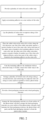
- some embodiments of the present disclosure provide a method for manufacturing a photovoltaic module. As shown in FIG. 1 and FIG. 2 , the manufacturing method includes the following steps.
- step S 1 a solar cell 1 and a solder strip 2 are provided, and the solar cell 1 is a back contact solar cell.
- a photovoltaic cell pack 100 of the photovoltaic module includes a plurality of solar cell strings 10.
- Each solar cell string 10 includes a plurality of solar cells 1 arranged at intervals. Two adjacent solar cells 1 are connected through the solder strip 2.
- step S2 an insulating adhesive 11 is applied on a rear surface of the solar cell 1.
- the solar cell 1 is a back contact solar cell, and a positive electrode and a negative electrode thereof are both arranged on a rear surface, which can reduce light blocking on the front surface and improve cell efficiency. Since the positive electrode and the negative electrode are on a same surface, the insulating adhesive 11 is required to be applied to prevent connection between positive and negative electrodes of a same solar cell caused by simultaneous contact of the solder strip with the positive electrode and the negative electrode, thereby achieving the purpose of preventing short circuit of the solar cell 1.
- step S3 a plurality of solar cells 1 are laid in sequence along a first direction X.
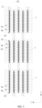
- a plurality of solar cells 1 are laid at intervals in sequence along the first direction X, and a positive busbar 12 of any solar cell 1 is aligned, along the first direction X, with a negative busbar 13 of another solar cell 1 adjacent thereto.
- step S4 the solder strip 2 is placed on the solar cells 1, and along the first direction X, one end of the solder strip 2 abuts against a positive busbar 12 of one of the solar cells 1, and at least part of the solder strip 2 is bonded to the insulating adhesive 11 on the solar cell 1.
- the other end of the solder strip 2 abuts against a negative busbar 13 of the other of the solar cells 1 adjacent thereto, and at least part of the solder strip 2 is bonded to the insulating adhesive 11 on the solar cell 1.
- the solder strip 2 is horizontally placed on surfaces of two adjacent solar cells 1 along the first direction X, and two ends of the solder strip 2 abut against the positive busbar 12 of one solar cell 1 and the negative busbar 13 of the other solar cell respectively for electrical connection, so that the two adjacent solar cells 1 are electrically connected.
- the solder strip 2 is also required to be bonded and fixed to the insulating adhesive 11 on the solar cell 1.
- the solder strip 2 may be placed by using a series soldering machine, which is more efficient and able to ensure accuracy of the placement of the solder strip 2.
- step S5 the insulating adhesive 11 is cured by irradiation with an ultraviolet lamp, to fixedly connect the solder strip 2 to the solar cell 1, so that the plurality of solar cells 1 are connected through the solder strip 2 to form solar cell strings 10.
- the plurality of solar cell strings 10 are arranged along a second direction Y, and two adjacent solar cell strings 10 are connected in series and/or in parallel to form a photovoltaic cell pack 100.
- the solder strip 2 can be fixed to the solar cell 1, which improves reliability of the connection between the solder strip 2 and the solar cell 1.
- a plurality of solder strips 2 are required to connect two adjacent solar cells 1 (the quantity of the solder strip 2 corresponds to the quantity of the positive busbar 12 and the quantity of the negative busbar 13), and the plurality of solar cells 1 are finally connected in series to form a solar cell string 10.
- the plurality of solar cell strings 10 are arranged along the second direction Y, and are connected through a busbar to form the photovoltaic cell pack 100.
- step S6 a front packaging structure 200 and a back packaging structure 300 are provided.
- the front packaging structure 200 includes a cover plate 201 and a front packaging adhesive film 202
- the back packaging structure 300 includes a back plate 301 and a back packaging adhesive film 302.
- the cover plate 201 and/or the back plate 301 may be made of one of rigid materials such as tempered glass, Polyethylene Terephthalate (PET), and Polycarbonate (PC), or made of one of flexible materials such as Polyvinyl Fluoride (PVF), Ethylene-Tetra-Fluoro-Ethylene (ETFE), and Polyvinylidene Fluoride (PVDF).
- PVDF Polyvinylidene Fluoride
- the front packaging adhesive film 202 and the back packaging adhesive film 302 may be made of one of materials such as Ethylene-Vinyl Acetate Copolymer (EVA), Polyolefin Elastomer (POE), and Polyvinyl Butyral (PVB).
- EVA Ethylene-Vinyl Acetate Copolymer
- POE Polyolefin Elastomer
- PVB Polyvinyl Butyral
- step S7 the front packaging structure 200 is arranged on a front surface of the photovoltaic cell pack 100, the back packaging structure 300 is arranged on a rear surface of the photovoltaic cell pack 100, and the front packaging structure 200, the photovoltaic cell pack 100, and the back packaging structure 300 are laminated to form the photovoltaic module.
- the front surface refers to the sunlight receiving surface of the photovoltaic cell
- the rear surface refers to the surface facing away from sunlight.
- Lamination is to bond and fuse various components of the photovoltaic module together under certain temperature, pressure, and vacuum conditions, so as to protect the photovoltaic cell pack 100.
- the fixed connection between the solder strip 2 and the solar cell 1 is realized by using the insulating adhesive 11, which, compared with the manner of connecting the solder strip 2 to the solar cell 1 by soldering in the related art, can prevent warping of the solar cell 1 caused by a transient high temperature to maintain structural stability of the solar cell 1, and then prevent hidden cracks and even splitting in subsequent procedures of the photovoltaic module, thereby helping to improve the yield of the photovoltaic module.
- "applying an insulating adhesive 11" is a necessary step in the manufacturing of the photovoltaic module.
- the solder strip 2 is laid when the insulating adhesive 11 is applied on a surface of the solar cell 1 and is not cured, the position of the solder strip 2 is first determined by using viscosity of the insulating adhesive 11, and then the insulating adhesive 11 is cured by irradiation with the ultraviolet lamp, so as to fix the solder strip 2.
- the solder strip 2 is connected to the solar cell 1 by soldering, there is a need to first cure the insulating adhesive 11 and then apply solder paste to the positive busbar 12 and/or the negative busbar 13.
- the method of the present disclosure can save manufacturing procedures, reduce manufacturing difficulty of the photovoltaic module, improve manufacturing efficiency of the photovoltaic module, save materials, and reduce the manufacturing cost of the photovoltaic module.
- the second direction Y is perpendicular to the first direction X.
- the first direction X may be a length direction of the solar cell string 10
- the second direction Y may be a width direction of the solar cell string 10.
- step S2 of applying an insulating adhesive 11 on a rear surface of the solar cell 1 the manufacturing method includes:
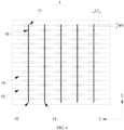
- the positive electrode includes the positive busbar 12 and the positive fingers 14, and two sides of the positive busbar 12 along the second direction Y are respectively connected to a plurality of positive fingers 14.
- the negative electrode includes the negative busbar 13 and the negative fingers 15, and two sides of the negative busbar 13 along the second direction Y are respectively connected to a plurality of negative fingers.
- the positive fingers 14 and the negative fingers 15 are respectively configured to collect currents in a cell diffusion layer and transfer the currents to the positive busbar 12 and the negative busbar 13.
- the positive busbar 12 and the negative busbar 13 are configured to transmit the currents collected from the positive fingers 14 and the negative fingers 15 to the outside of the solar cell 1.
- the positive busbar 12 is closer to the negative fingers 15 on the two sides thereof. Therefore, there is a need to apply the insulating adhesive 11 on one end of the negative fingers 15 close to the positive busbar 12. Similarly, the insulating adhesive 11 is further required to be applied on one end of the positive fingers 14 close to the negative busbar 13. In this way, even if the solder strip 2 slightly deviates during the placement and contacts the positive electrode and the negative electrode on a same solar cell 1 at the same time (contacts the positive busbar 12 and the negative fingers 15 at the same time or contacts the positive fingers 14 and the negative busbar 13 at the same time), the solar cell 1 may not be short circuited, which improves the yield of the photovoltaic module.
- the positive busbar 12 and/or the negative busbar 13 are/is connected to a body of the solar cell 1 through electrode pads 16.
- the electrode pads 16 are arranged at intervals along the first direction X and can be electrically connected to the solder strip 2.
- the solder strip 2 can completely fit the electrode pad 16 to ensure the electrical connection between the solder strip 2 and the solar cell 1.
- the electrical connection between the solder strip 2 and the solar cell 1 may not be affected.
- the thickness H1 of the applied insulating adhesive 11 is greater than 30 ⁇ m.
- H1 may be, for example, 30 ⁇ m, 32 ⁇ m, 35 ⁇ m, 40 ⁇ m, 44 ⁇ m, 48 ⁇ m, 50 ⁇ m, 53 ⁇ m, 59 ⁇ m, 65 ⁇ m, or 70 ⁇ m, or other values in the above range, which is not limited in the present disclosure.
- the thickness H1 of the applied insulating adhesive 11 is excessively small (e.g., less than or equal to 30 ⁇ m), when the solder strip 2 is placed, stable contact between the solder strip 2 and the insulating adhesive 11 cannot be ensured, which may affect stability of the connection between the solder strip 2 and the solar cell 1.
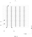
- the insulating adhesive 11 When applied, the insulating adhesive 11 may be applied consecutively along the first direction X (as shown in FIG. 13 ), or applied at intervals along the first direction X (as shown in FIG. 14 ). In this regard, it should be guaranteed that the insulating adhesive 11 is applied on one end of each negative finger 15 close to the positive busbar 12 and the insulating adhesive 11 is applied on one end of each positive finger 14 close to the negative busbar 13.
- the insulating adhesive 11 is applied at intervals in the first direction X and there is a need to minimize the usage amount of the insulating adhesive 11. For example, as shown in FIG. 4 , along the first direction X, an applying width W1 of the insulating adhesive 11 at each position ranges from 200 ⁇ m to 600 ⁇ m.
- W1 may be, for example, 200 ⁇ m, 230 ⁇ m, 250 ⁇ m, 300 ⁇ m, 350 ⁇ m, 400 ⁇ m, 440 ⁇ m, 480 ⁇ m, 500 ⁇ m, 550 ⁇ m, 570 ⁇ m, or 800 ⁇ m, or other values in the above range, which is not limited in the present disclosure.
- an applying length L1 of the insulating adhesive 11 is determined, if the applying width W1 of the insulating adhesive 11 is excessively small (e.g., less than 200 ⁇ m), applying areas of the insulating adhesive 11 on the positive finger 14 and/or the negative finger 15 may be excessively small, thereby leading to an insufficient connection area between the solar cell 1 and the solder strip 2 and affecting stability of the connection with the solder strip 2. If the applying width W1 of the insulating adhesive 11 is excessively large (e.g., greater than 600 ⁇ m), the insulation effect or the stability of the connection with the solder strip 2 may not be improved, but the insulating adhesive 11 may be wasted, resulting in an increase in the weight and the cost of the photovoltaic module.
- the applying width W1 of the insulating adhesive 11 is excessively small (e.g., less than 200 ⁇ m)
- applying areas of the insulating adhesive 11 on the positive finger 14 and/or the negative finger 15 may be excessively small, thereby leading to an insufficient connection
- the applying length L1 of the insulating adhesive 11 at each position ranges from 800 ⁇ m to 1200 ⁇ m.
- L1 may be, for example, 800 ⁇ m, 820 ⁇ m, 850 ⁇ m, 880 ⁇ m, 900 ⁇ m, 930 ⁇ m, 970 ⁇ m, 1000 ⁇ m, 1050 ⁇ m, 1080 ⁇ m, 1100 ⁇ m, 1120 ⁇ m, 1150 ⁇ m, or 1200 ⁇ m, or other values in the above range, which is not limited in the present disclosure.
- the applying width W1 of the insulating adhesive 11 is determined, if the applying length L1 of the insulating adhesive 11 is excessively small (e.g., less than 800 ⁇ m), applying areas of the insulating adhesive 11 on the positive finger 14 and/or the negative finger 15 may be excessively small, thereby leading to an insufficient connection area between the solar cell 1 and the solder strip 2 and affecting stability of the connection with the solder strip 2. If the applying length L1 of the insulating adhesive 11 is excessively large (e.g., greater than 1200 ⁇ m), the insulation effect or the stability of the connection with the solder strip 2 may not be improved, but the insulating adhesive 11 may be wasted, resulting in an increase in the weight and the cost of the photovoltaic module.
- the applying length L1 of the insulating adhesive 11 is excessively small (e.g., less than 800 ⁇ m)
- applying areas of the insulating adhesive 11 on the positive finger 14 and/or the negative finger 15 may be excessively small, thereby leading to an insufficient
- the applying length L1 of the insulating adhesive 11 ranges from 800 ⁇ m to 1200 ⁇ m and the applying width W1 ranges from 200 ⁇ m to 600 ⁇ m, the stability of the connection between the solder strip 2 and the solar cell 1 can be ensured, and the weight and the manufacturing cost of the photovoltaic module can be appropriately reduced.
- the insulating adhesive 11 may be one or more of silicone, acrylic acid, and epoxy resin. "Applying an insulating adhesive 11" may be attaching, by screen printing, a template with a pattern to a screen for applying the insulating adhesive.
- the solar cell 1 is placed under the screen with the template, and the insulating adhesive 11 passes through meshes in the middle of the screen under extrusion of a scraper and is applied on the rear surface of the solar cell 1.
- the template on the screen seals part of small holes of the screen, and the insulating adhesive 11 cannot pass therethrough. Therefore, only the position corresponding to the pattern of the screen on the solar cell 1 (the negative fingers 15 on two sides of the positive busbar 12 and/or the positive fingers 14 on two sides of the negative busbar 13) is coated with the insulating adhesive 11.
- applying an insulating adhesive may alternatively be using, by mask printing, a mask applied with a pattern for applying the insulating adhesive.
- the principle and the effect are the same as those of screen printing. Details are not described herein again.
- step S4 of abutting the solder strip 2 against a positive busbar 12 and bonding at least part of the solder strip 2 to the insulating adhesive 11 on the solar cell 1 the manufacturing method includes: bonding, along the second direction Y, two sides of the solder strip 2 respectively to the insulating adhesive 11 on the negative fingers 15 on the two sides of the positive busbar 12.
- the manufacturing method includes: bonding, along the second direction Y, two sides of the solder strip 2 respectively to the insulating adhesive 11 on the positive fingers 14 on the two sides of the negative busbar 13.
- L2 lengths of bonding of two sides of the solder strip 2 to the insulating adhesive 11 are both L2, and L2 ranges from 0.1 mm to 0.2 mm.
- L2 may be, for example, 0.1 mm, 0.11 mm, 0.12 mm, 0.13 mm, 0.14 mm, 0.15 mm, 0.16 mm, 0.17 mm, 0.18 mm, 0.19 mm, or 0.2 mm, or other values in the above range, which is not limited in the present disclosure.
- the length of bonding L2 is excessively small (e.g., less than 0.1 mm), a connection area between the solder strip 2 and the solar cell 1 may be insufficient, which affects the stability of the connection with the solder strip 2.
- the length of bonding L2 is excessively large (e.g., greater than 0.2 mm)
- a solder strip 2 with a larger width is required, but the widened solder strip 2 may lead to an increase in the cost of the photovoltaic module.
- the width of the solder strip 2 remains unchanged, an applying position of the insulating adhesive 11 is required to be set closer to the positive busbar 12 and/or the negative busbar 13. However, this may increase applying difficulty of the insulating adhesive and easily lead to defective photovoltaic modules.
- the lengths of bonding L2 between the two sides of the solder strip 2 and the insulating adhesive 11 range from 0.1 mm to 0.2 mm, the stability of the connection between the solder strip 2 and the insulating adhesive 11 can be ensured, and the yield of the photovoltaic module can be improved.
- irradiation time of the ultraviolet lamp ranges from 0.2 s to 0.8 s, which may be, for example, 0.2 s, 0.25 s, 0.3 s, 0.35 s, 0.4 s, 0.45 s, 0.5 s, 0.55 s, 0.6 s, 0.65 s, 0.7 s, 0.75 s, or 0.8 s, or other values in the above range, which is not limited in the present disclosure.
- the insulating adhesive 11 cannot be completely cured, thereby leading to an insufficiently strong connection between the solar cell 1 and the solder strip 2. If the irradiation time of the ultraviolet lamp is excessively long (e.g., longer than 0.8 s), the curing has been completed, which may not improve the curing effect but may lead to reduction in manufacturing efficiency of the photovoltaic module.
- the irradiation time of the ultraviolet lamp ranges from 0.2 s to 0.8 s, which can improve the manufacturing efficiency of the photovoltaic module on the basis of ensuring that the solder strip 2 can be firmly connected to the solar cell 1.
- irradiance of the ultraviolet lamp ranges from 500 m ⁇ W/cm 2 to 1000 m ⁇ W/cm 2 , which may be, for example, 500 m ⁇ W/cm 2 , 550 m ⁇ W/cm 2 , 600 m ⁇ W/cm 2 , 650 m ⁇ W/cm 2 , 700 m ⁇ W/cm 2 , 750 m ⁇ W/cm 2 , 800 m ⁇ W/cm 2 , 850 m ⁇ W/cm 2 , 900 m ⁇ W/cm 2 , 950 m ⁇ W/cm 2 , or 1000 m ⁇ W/cm 2 , or other values in the above range, which is not limited in the present disclosure.
- the irradiance refers to radiation flux per unit area of an illuminated surface. If the irradiance of the ultraviolet lamp is excessively low (e.g., less than 500 m ⁇ W/cm 2 ), in order to ensure the curing effect of the insulating adhesive 11, the irradiation time of the ultraviolet lamp is required to be extended, which leads to a decrease in the efficiency of the curing step. If the irradiance of the ultraviolet lamp is excessively high (e.g., greater than 1000 m ⁇ W/cm 2 ), energy consumption of the ultraviolet lamp may be excessively large, thereby leading to an increase in the manufacturing cost of the photovoltaic module.
- the irradiance of the ultraviolet lamp ranges from 500 m ⁇ W/cm 2 to 1000 m ⁇ W/cm 2 , which can improve the manufacturing efficiency of the photovoltaic module and can also appropriately reduce the manufacturing cost of the photovoltaic module.
- the manufacturing method further includes the following steps.
- step A1 a reinforcing adhesive 3 is applied to an exposed surface of the solder strip 2, so that at least part of the reinforcing adhesive 3 is bonded to the insulating adhesive 11 and/or the rear surface of the solar cell 1.
- the reinforcing adhesive 3 is provided on a surface of the solder strip 2 that is not in contact with the positive busbar 12 and/or the negative busbar 13 and the insulating adhesive 11 to wrap the solder strip 2.
- step A2 the reinforcing adhesive 3 is cured by irradiation with the ultraviolet lamp.
- the cured reinforcing adhesive 3 can wrap the solder strip 2, which restricts movement of the solder strip 2 along a thickness direction Z of the solar cell 1, enables the mutual tension force between the solder strip 2 and the solar cell 1, further improves the stability of the connection between the solder strip 2 and the solar cell 1, and prevents falling off of the solder strip 2 from the solar cell 1.
- the manufacturing method further includes the following steps.
- step B1 adhesive deviation inspection is performed on the solar cell 1 on which the insulating adhesive 11 is applied.
- the adhesive deviation inspection is mainly to check an adhesive application result of the insulating adhesive 11 to see whether there is adhesive position deviation, adhesive shortage, adhesive breakage, or adhesive overflow.
- manual visual inspection may be replaced with an auto optical inspection (AOI) process, i.e., by an auto optical detector, so as to improve inspection efficiency and accuracy of inspection results.
- AOI auto optical inspection
- step B2 appearance inspection is performed on the solar cell 1.
- the appearance inspection is mainly to inspect the thickness, defects, flatness, and the like of the solar cell 1. At the same time, the color of the solar cell 1 should remain uniform without any obvious color difference.
- the manufacturing method further includes the following steps.
- step B3 the solar cell 1 is scribed into half-cut cells.
- the photovoltaic module is generally manufactured by using the half-cut cells. That is, a complete cell is cut by laser into two half-cells, and the half-cells are the half-cut cells.
- step B4 front appearance inspection and back appearance inspection are performed on the half-cut cells.
- Thicknesses, defects, flatness, and the like of the half-cut cells are inspected, to ensure that there are no scratches or splits and that the membrane is not dirty.
- the solar cell 1 used to manufacture the solar cell string 10 may be a whole cell or half-cut cells.
- step A1 of applying a reinforcing adhesive 3 to an exposed surface of the solder strip 2 the manufacturing method includes: applying, along the first direction X, the reinforcing adhesive 3 intermittently to the solder strip 2.
- the reinforcing adhesive 3 is not required to be applied to an entire outer surface of the solder strip 2, and the effect of reinforcing the solder strip 2 can be achieved by intermittent application.
- a distance L3 between the reinforcing adhesive 3 at two adjacent positions ranges from 2 mm to 10 mm.
- L3 may be, for example, 2 mm, 3 mm, 4 mm, 5 mm, 6 mm, 7 mm, 8 mm, 9 mm, or 10 mm, or other values in the above range, which is not limited in the present disclosure.
- the distance L3 between the reinforcing adhesive 3 at two adjacent positions is excessively large (e.g., greater than 10 mm), the area of the applied reinforcing adhesive 3 may be insufficient, resulting in a non-ideal reinforcing effect of the reinforcing adhesive 3 on the solder strip 2. If the distance L3 between the reinforcing adhesive 3 at two adjacent positions is excessively small (e.g., less than 2 mm), the reinforcing effect of the reinforcing adhesive 3 on the solder strip 2 may no longer be improved, and the reinforcing adhesive 3 may be wasted, resulting in an increase in the weight and the cost of the photovoltaic module.
- the distance L3 between the reinforcing adhesive 3 at two adjacent positions ranges from 2 mm to 10 mm, which can ensure the reinforcing effect of the reinforcing adhesive 3 on the solder strip 2 and can also save the usage amount of the reinforcing adhesive 3, thereby preventing waste of material and appropriately reducing the weight and the cost of the photovoltaic module.
- the thickness H3 of the applied reinforcing adhesive 3 ranges from 50 ⁇ m to 300 ⁇ m.
- H3 may be, for example, 50 ⁇ m, 80 ⁇ m, 100 ⁇ m, 120 ⁇ m, 150 ⁇ m, 180 ⁇ m, 200 ⁇ m, 230 ⁇ m, 260 ⁇ m, 290 ⁇ m, or 300 ⁇ m, or other values in the above range, which is not limited in the present disclosure.
- the application thickness H3 of the reinforcing adhesive 3 is excessively small (e.g., less than 50 ⁇ m), stable contact between the reinforcing adhesive 3 and the insulating adhesive 11 and/or the rear surface of the solar cell 1 cannot be ensured, and after the reinforcing adhesive 3 is cured, the reinforcing adhesive 3 may easily fall off, which affects the reinforcing effect of the reinforcing adhesive 3. If the application thickness H3 of the reinforcing adhesive 3 is excessively large (e.g., greater than 300 ⁇ m), the curing effect of the solder strip 2 may not be improved, but the reinforcing adhesive 3 may be wasted, resulting in an increase in the weight, the thickness, and the cost of the photovoltaic module.
- the application thickness H3 of the reinforcing adhesive 3 ranges from 50 ⁇ m to 300 ⁇ m, the reinforcing effect of the reinforcing adhesive 3 on the connection between the solder strip 2 and the solar cell 1 can be ensured, and the usage amount of the reinforcing adhesive 3 can be saved, thereby preventing waste of material and appropriately reducing the weight, the thickness, and the cost of the photovoltaic module.
- the reinforcing adhesive 3 is a light-curing adhesive, which may be, for example, made of silicone and acrylic resin.
- the acrylic resin includes, but is not limited to, epoxy acrylate, polyurethane acrylate, polyester acrylate, polyether acrylate, acrylated acrylate resin or vinyl resin, and the like.
- irradiation time of the ultraviolet lamp ranges from 2 s to 6 s, which may be, for example, 2 s, 2.5 s, 3 s, 3.5 s, 4 s, 4.5 s, 5 s, 5.5 s, or 6 s, or other values in the above range, which is not limited in the present disclosure.
- the area of the applied reinforcing adhesive 3 is larger than that of the insulating adhesive 11, it takes a longer irradiation time to cure the reinforcing adhesive 3.
- the irradiation time of the ultraviolet lamp is excessively short (e.g., shorter than 2 s)
- the reinforcing adhesive 3 cannot be completely cured, and strength of the connection between the solder strip 2 and the solar cell 1 cannot be further improved.
- the irradiation time of the ultraviolet lamp is excessively long (e.g., longer than 6 s), the curing has been completed, which may not improve the curing effect but may lead to reduction in manufacturing efficiency of the photovoltaic module.
- the irradiation time of the ultraviolet lamp ranges from 2 s to 6 s, which can improve the manufacturing efficiency of the photovoltaic module on the basis of ensuring that the reinforcing adhesive 3 has been completely cured.
- irradiance of the ultraviolet lamp ranges from 1000 m ⁇ W/cm 2 to 2000 m ⁇ W/cm 2 , which may be, for example, 1000 m ⁇ W/cm 2 , 1100 m W/cm 2 , 1200 m ⁇ W/cm 2 , 1300 m ⁇ W/cm 2 , 1400 m ⁇ W/cm 2 , 1500 m ⁇ W/cm 2 , 1600 m ⁇ W/cm 2 , 1700 m ⁇ W/cm 2 , 1800 m ⁇ W/cm 2 , 1900 m ⁇ W/cm 2 , or 2000 m ⁇ W/cm 2 , or other values in the above range, which is not limited in the present disclosure.
- the irradiance of the ultraviolet lamp is excessively low (e.g., less than 1000 m ⁇ W/cm 2 ), in order to ensure the curing effect of the reinforcing adhesive 3, the irradiation time of the ultraviolet lamp is required to be extended, which leads to a decrease in the efficiency of the curing step. If the irradiance of the ultraviolet lamp is excessively high (e.g., greater than 2000 m ⁇ W/cm 2 ), energy consumption of the ultraviolet lamp may be excessively large, thereby leading to an increase in the manufacturing cost of the photovoltaic module.
- the irradiance of the ultraviolet lamp ranges from 1000 m ⁇ W/cm 2 to 2000 m ⁇ W/cm 2 , which can improve the manufacturing efficiency of the photovoltaic module and can also appropriately reduce the manufacturing cost of the photovoltaic module.
- an irradiation temperature of the ultraviolet lamp ranges from 200tovoltai°Cn some embodiments, for step S5 and/or step A2, an irradiation temperature of the ultraviolet lamp ranges from 200tovoltaic module.not limited in the present disclosure.
- the temperature is excessively low (e.g., less than 200ation temperature of the ultraviolfor the insulating adhesive 11 and/or the reinforcing adhesive 3 may be extended, which reduces efficiency of the curing step.
- the temperature is excessively high (e.g., greater than 400000 m W/cm is excessively long (e.g., longer than 6 s), the curing e/is prone to dehydration and failure due to a high temperature.
- the irradiation temperature of the ultraviolet lamp ranges from 200hich reduces efficiency of the curing step. If the temperature is excessivimproved, and the yield of the photovoltaic module can also be improved.
- an infrared soldering head of the existing series soldering machine is replaced by a UV light box, so step S5 and/or step A2 may be performed in the UV light box.
- a finished UV light box may alternatively be used, which is not limited in the present disclosure.
- the photovoltaic module includes a photovoltaic cell pack 100, a front packaging structure 200, and a back packaging structure 300.
- the photovoltaic cell pack 100 includes a plurality of solar cell strings 10 arranged along the second direction Y
- the front packaging structure 200 is arranged on the front surface of the photovoltaic cell pack 100.
- the back packaging structure 300 is arranged on the rear surface of the photovoltaic cell pack 100.
- Each of the solar cell strings 10 includes a plurality of solar cells 1 arranged in sequence along a first direction X, and the solar cells 1 are back contact solar cells.
- Each of the solar cell strings 10 further includes a solder strip 2. Along the first direction X, two ends of the solder strip 2 are bonded and fixed to two adjacent solar cells 1 through an insulating adhesive 11, so that the two adjacent solar cells 1 are connected in series through the solder strip 2.
- the solder strip 2 connects the plurality of solar cells 1 in series to form one solar cell string 10.
- the plurality of solar cell strings 10 are connected in series/parallel to form the photovoltaic cell pack 100.
- the insulating adhesive 11 can also be used to fix the solder strip 2 to ensure stable contact of the solder strip 2 with the positive busbar 12 and/or the negative busbar 13 of the solar cell 1.
- the insulating adhesive 11, after being applied on the rear surface of the solar cell 1, may be immediately formed through a high-temperature curing treatment.
- solder strip 2 and the insulating adhesive 11 are not connected by bonding, and the solder strip 2 is fixed to the positive busbar 12 and/or the negative busbar 13 by soldering.
- the connection between the solder strip 2 and the busbar by bonding is replaced by the connection between the insulating adhesive 11 and the solder strip 2 through bonding, which can prevent warping of the solar cell 1 and help to improve the yield of the photovoltaic module.
- the photovoltaic module provided according to the present disclosure can save manufacturing procedures, reduce manufacturing difficulty of the photovoltaic module, improve manufacturing efficiency of the photovoltaic module, save materials, and thus reduce the manufacturing cost of the photovoltaic module.
- a positive busbar 12 of any one of the solar cells 1 is aligned with a negative busbar 13 of the other one of the solar cells 1 adjacent thereto, and along the first direction X, the solder strip 2 has one end abutting against the positive busbar 12 of one of the solar cells 1 and the other end abutting against the negative busbar 13 of the other one of the solar cells 1 adjacent thereto.
- the insulating adhesive 11 is provided on negative fingers 15 on two sides of the positive busbar 12 and/or positive fingers 14 on two sides of the negative busbar 13. In this way, short circuit of the solar cell 1 can be effectively prevented, and the yield of the photovoltaic module is improved.
- the insulating adhesive 11 may be applied consecutively along the first direction X (as shown in FIG. 13 ), or applied at intervals along the first direction X (as shown in FIG. 14 and FIG. 4 ). In this regard, it should be guaranteed that the insulating adhesive 11 is provided on one end of each negative finger 15 close to the positive busbar 12 and the insulating adhesive 11 is provided on one end of each positive finger 14 close to the negative busbar 13.
- the lengths of bonding L2 between the two sides of the solder strip 2 and the insulating adhesive 11 are both L2, and L2 ranges from 0.1 mm to 0.2 mm, which can ensure a good bonding effect of the solder strip 2 and the insulating adhesive 11, and can maintain a stable connection, and thus improve the yield of the photovoltaic module.
- the solar cell string 10 further includes a reinforcing adhesive 3, and along the first direction X.
- the reinforcing adhesive 3 is provided at intervals on an outer surface of the solder strip 2, and at least part of the reinforcing adhesive 3 is fixedly connected to the insulating adhesive 11 and/or the rear surface of the solar cell 1.
- a distance L3 between the reinforcing adhesive 3 at two adjacent positions ranges from 2 mm to 10 mm.
- the reinforcing adhesive 3 covers the outer surface of the solder strip 2, with two ends bonded to the insulating adhesive 11 and/or the rear surface of the solar cell 1, which prevents falling off of the cured reinforcing adhesive 3 from the surface of the solder strip 2.
- the cured reinforcing adhesive 3 can wrap the solder strip 2, which restricts movement of the solder strip 2 along a thickness direction Z of the solar cell 1, thus enables a mutual tension force between the solder strip 2 and the solar cell 1, further improves the stability of the connection between the solder strip 2 and the solar cell 1, and thereby preventing falling off of the solder strip 2 from the solar cell 1.
- the distance L3 between the reinforcing adhesive 3 at two adjacent positions ranges from 2 mm to 10 mm, the reinforcing effect of the reinforcing adhesive 3 on the solder strip 2 can be ensured, and the usage amount of the reinforcing adhesive 3 can be saved, thereby preventing waste of material and appropriately reducing the weight and the cost of the photovoltaic module.
- the solder strip 2 is one of a circular solder strip, a rectangular solder strip, and a T-shaped solder strip, or in other shapes, which is not limited in the present disclosure. It should be made clear that the shape of the solder strip refers to the shape of the cross-section of the solder strip.
- a diameter D1 thereof ranges from 160 ⁇ m to 1000 ⁇ m, which may be, for example, 160 ⁇ m, 200 ⁇ m, 250 ⁇ m, 300 ⁇ m, 350 ⁇ m, 400 ⁇ m, 450 ⁇ m, 500 ⁇ m, 550 ⁇ m, 600 ⁇ m, 650 ⁇ m, 700 ⁇ m, 750 ⁇ m, 800 ⁇ m, 850 ⁇ m, 900 ⁇ m, 950 ⁇ m, or 1000 ⁇ m, or other values in the above range, which is not limited in the present disclosure.
- the diameter D1 is excessively small (e.g., less than 160 ⁇ m), the solder strip 2 cannot be bonded to the insulating adhesive 11 on the two sides of the positive busbar 12 and/or the negative busbar 13, or the bonding area is excessively small, which results in insufficient stability of the connection between the solder strip 2 and the solar cell 1. If the diameter D1 is excessively large (e.g., greater than 1000 ⁇ m), it is not convenient to laminate the photovoltaic module.
- the diameter D1 of the circular solder strip ranges from 160 ⁇ m to 1000 ⁇ m, the stability of the connection between the solder strip 2 and the solar cell 1 can be ensured, without affecting the subsequent lamination step of the photovoltaic module.
- the solder strip 2 has small hardness, and the circular solder strip can be deformed into an oval shape by pressing, so as to increase the area of contact with the insulating adhesive 11 and facilitate bonding between the two.
- a height H2 thereof ranges from 260 ⁇ m to 1200 ⁇ m, which may be, for example, 260 ⁇ m, 300 ⁇ m, 350 ⁇ m, 400 ⁇ m, 450 ⁇ m, 500 ⁇ m, 550 ⁇ m, 600 ⁇ m, 650 ⁇ m, 700 ⁇ m, 750 ⁇ m, 800 ⁇ m, 850 ⁇ m, 900 ⁇ m, 950 ⁇ m, 1000 ⁇ m, 1050 ⁇ m, 1100 ⁇ m, 1150 ⁇ m, or 1200 ⁇ m, or other values in the above range, which is not limited in the present disclosure.
- the solder strip 2 has insufficient strength is prone to breakage during the manufacturing, which affects the use of the solar cell 1. If the height H2 is excessively large (e.g., greater than 1200 ⁇ m), it is not convenient to laminate the photovoltaic module.
- the height H2 of the T-shaped solder strip or the rectangular solder strip ranges from 260 ⁇ m to 1200 ⁇ m, strength of the solder strip 2 can be improved, without affecting the subsequent lamination step of the photovoltaic module.
- part of the insulating adhesive 11 may half-wrap the solder strip 2 from two sides of the solder strip 2 along the second direction Y, so as to further improve the strength of the bonding between the solder strip 2 and the insulating adhesive 11, thereby improving the stability of the connection between the solder strip 2 and the solar cell 1.
- the solder strip 2 when the solder strip 2 is the T-shaped solder strip, the solder strip 2 includes a main body portion 21 and an abutting portion 22.
- the main body portion 21 is configured to be bonded to the insulating adhesive 11 along the second direction Y.
- the abutting portion 22 is configured to abut against the positive busbar 12 and/or the negative busbar 13.
- the abutting portion 22 is located between the insulating adhesive 11 on two sides, which can increase the bonding area of the solder strip 2 and the insulating adhesive 11, so that the connection between the solder strip 2 and the solar cell 1 is firmer.
- the dimension of the abutting portion 22 in the second direction Y is less than the distance between the insulating adhesive 11 at two positions, so that a certain gap can be maintained between the abutting portion 22 and the insulating adhesive 11 to enable the abutting portion 22 to be smoothly placed at the position between portions applied with the insulating adhesive 11.
Landscapes
- Photovoltaic Devices (AREA)
Abstract
Description
- The present disclosure relates to the field of photovoltaic technologies, and in particular, to a method for manufacturing a photovoltaic module and a photovoltaic module.
- Solar energy is an inexhaustible renewable energy source for human beings. A photovoltaic module is a core part in a solar power generation system and is also the most important part in the solar power generation system, whose function is to convert solar energy into electrical energy and send the electrical energy to a storage battery for storage or drive a load into operation. The photovoltaic module generally includes a front packaging structure, a back packaging structure, and a photovoltaic cell pack. The photovoltaic cell pack is formed by a plurality of solar cell strings connected in series or in parallel. Each solar cell string includes a plurality of solar cells arranged at intervals, and two adjacent solar cells are connected through a solder strip.
- In the related art, the solder strip is fixedly connected to the solar cell by soldering. For a conventional solar cell, front and back surfaces thereof are required to be provided with a solder strip, which can offset soldering stress. However, for a back contact solar cell, positive and negative electrodes thereof are both located on the back surface, and soldering stress cannot be eliminated, which may lead to warping of the solar cell, thereby increasing the defective rate of the photovoltaic module.
- The present disclosure provides a method for manufacturing a photovoltaic module, and a photovoltaic module, which can reduce the possibility of warping of a back contact solar cell during the arrangement of the solder strip.
- In a first aspect of the present disclosure, a method for manufacturing a photovoltaic module is provided, the method includes the following steps: providing a plurality of solar cells and a solder strip, the solar cells are a back contact solar cell; applying an insulating adhesive on a rear surface of the solar cells; laying the plurality of solar cells in sequence along a first direction; placing the solder strip on the solar cells so that, along the first direction, one end of the solder strip abuts against a positive busbar of one of the solar cells, and at least part of the solder strip is bonded to the insulating adhesive on the solar cells; and the other end of the solder strip abuts against a negative busbar of another one of the solar cells adjacent thereto, and at least part of the solder strip is bonded to the insulating adhesive on the solar cell; curing the insulating adhesive by irradiation with an ultraviolet lamp to fixedly connect the solder strip to the solar cells, so that the plurality of solar cells are connected through the solder strip to form a solar cell string; arranging a plurality of formed solar cell strings along a second direction, and connecting two adjacent solar cell strings in series and/or in parallel to form a photovoltaic cell pack, the second direction is perpendicular to the first direction; providing a front packaging structure and a back packaging structure; and arranging the front packaging structure on a front surface of the photovoltaic cell pack, arranging the back packaging structure on a rear surface of the photovoltaic cell pack, and laminating the front packaging structure, the photovoltaic cell pack, and the back packaging structure to form the photovoltaic module.
- In one or more embodiments, the applying an insulating adhesive on a rear surface of the solar cells includes: applying, along the second direction, the insulating adhesive on negative fingers on two sides of the positive busbar and/or positive fingers on two sides of the negative busbar.
- In one or more embodiments, the abutting the solder strip against a positive busbar and bonding at least part of the solder strip to the insulating adhesive on the solar cell includes: bonding, along the second direction, two sides of the solder strip respectively to the insulating adhesive on the negative fingers on the two sides of the positive busbar; and/or the abutting the solder strip against a negative busbar and bonding at least part of the solder strip to the insulating adhesive on the solar cell includes: bonding, along the second direction, two sides of the solder strip respectively to the insulating adhesive on the positive fingers on the two sides of the negative busbar.
- In one or more embodiments, in the curing the insulating adhesive by irradiation with an ultraviolet lamp, an irradiation time of the ultraviolet lamp ranges from 0.2 s to 0.8 s.
- In one or more embodiments, in the curing the insulating adhesive by irradiation with an ultraviolet lamp, an irradiance of the ultraviolet lamp ranges from 500 m·W/cm2 to 1000 m·W/cm2.
- In one or more embodiments, subsequent to the curing the insulating adhesive by irradiation with an ultraviolet lamp, the manufacturing method further includes: applying a reinforcing adhesive to an exposed surface of the solder strip, so that at least part of the reinforcing adhesive is bonded to the insulating adhesive and/or the rear surface of the solar cell; and curing the reinforcing adhesive by irradiation with the ultraviolet lamp.
- In one or more embodiments, the applying a reinforcing adhesive to an exposed surface of the solder strip includes: applying, along the first direction, the reinforcing adhesive intermittently on the solder strip.
- In one or more embodiments, in the curing the reinforcing adhesive by irradiation with the ultraviolet lamp, an irradiation time of the ultraviolet lamp ranges from 2 s to 6 s.
- In one or more embodiments, in the curing the reinforcing adhesive by irradiation with the ultraviolet lamp, an irradiance of the ultraviolet lamp ranges from 1000 m·W/cm2 to 2000 m·W/cm2.
- In a second aspect of the present disclosure, a photovoltaic module is provided, the photovoltaic module includes: a photovoltaic cell pack including a plurality of solar cell strings arranged along a second direction; a front packaging structure arranged on a front surface of the photovoltaic cell pack; and a back packaging structure arranged on a rear surface of the photovoltaic cell pack. Each of the solar cell strings includes a plurality of solar cells arranged in sequence along a first direction, and the solar cells are back contact solar cells. Each of the solar cell strings further includes a solder strip, and along the first direction, two ends of the solder strip are bonded and fixed to two adjacent solar cells through an insulating adhesive, so that the two adjacent solar cells are connected in series through the solder strip.
- In one or more embodiments, along the first direction, a positive busbar of any one of the solar cells is aligned with a negative busbar of another one of the solar cells adjacent thereto; and along the first direction, the solder strip includes one end abutting against the positive busbar of one of the solar cells and the other end abutting against the negative busbar of the another one of the solar cells adjacent thereto.
- In one or more embodiments, along the second direction, the insulating adhesive is provided on negative fingers on two sides of the positive busbar and/or positive fingers on two sides of the negative busbar; and along the second direction, lengths of bonding of two sides of the solder strip to the insulating adhesive are both L2, and L2 ranges from 0.1 mm to 0.2 mm.
- In one or more embodiments, each of the solar cell strings further includes a reinforcing adhesive, and along the first direction, the reinforcing adhesive is provided at intervals on an outer surface of the solder strip, and at least part of the reinforcing adhesive is fixedly connected to the insulating adhesive and/or a rear surface of the solar cell; and along the first direction, a distance L3 between the reinforcing adhesive at two adjacent positions ranges from 2 mm to 10 mm.
- In one or more embodiments, the solder strip is one of a circular solder strip, a rectangular solder strip, or a T-shaped solder strip.
- It should be understood that the general description above and the detailed description in the following are merely exemplary and illustrative, and cannot limit the present disclosure.
-
-
FIG. 1 is a schematic structural diagram of a photovoltaic module according to one or more embodiments of the present disclosure; -
FIG. 2 is a flowchart of manufacturing a photovoltaic module according to one or more embodiments of the present disclosure; -
FIG. 3 is a schematic structural diagram of a solar cell string inFIG. 1 ; -
FIG. 4 is a schematic structural diagram of the solar cells inFIG. 3 according to some embodiments; -
FIG. 5 is a sectional view ofFIG. 3 according to some embodiments; -
FIG. 6 is a flowchart of manufacturing a photovoltaic module according to one or more embodiments of the present disclosure; -
FIG. 7 is a schematic structural diagram the solar cell string inFIG. 3 after a reinforcing adhesive is applied; -
FIG. 8 is a sectional view ofFIG. 7 ; -
FIG. 9 is a flowchart of manufacturing a photovoltaic module according to one or more embodiments of the present disclosure; -
FIG. 10 is a flowchart of manufacturing a photovoltaic module according to one or more embodiments of the present disclosure; -
FIG. 11 is a sectional view ofFIG. 3 according to some embodiments; -
FIG. 12 is a sectional view ofFIG. 3 according to some embodiments; -
FIG. 13 is a schematic structural diagram of the solar cell string inFIG. 3 according to some embodiments; and -
FIG. 14 is a schematic structural diagram of the solar cell string inFIG. 3 according to some embodiments. - The accompanying drawings herein, which are incorporated in and constitute a part of this specification, illustrate embodiments consistent with the present disclosure and, together with the specification, serve to explain principles of the present disclosure.
- In order to better understand the technical solutions of the present disclosure, embodiments of the present disclosure will be described in detail below in conjunction with the accompanying drawings.
- It should be clear that the described embodiments are only some rather than all of the embodiments of the present disclosure.
- Terms used in the embodiments of the present disclosure are only for the purpose of describing specific embodiments, and are not intended to limit the present disclosure. Singular forms of "alan", "the", and "said" used in the embodiments of the present disclosure and the appended claims are intended to include plural forms, unless otherwise clearly specified in the context.
- It should be understood that the term "and/or" used herein describes an association relationship between associated objects and represents that three relationships may exist. For example, A and/or B may represent the following three cases: only A exists, both A and B exist, and only B exists. In addition, the character "/" herein generally indicates an "or" relationship between the associated objects.
- It is to be noted that orientation terms such as "above", "below", "left", and "right" described in the embodiments of the present disclosure are described from the perspective shown in the accompanying drawings, and should not be construed as limiting the embodiments of the present disclosure. Besides, in this context, it is to be further understood that one element described as being connected "above" or "below" another element not only means that the element may be directly connected "above" or "below" the other element, but also means that the element may be indirectly connected "above" or "below" the other element through an intermediate element.
- In an existing method for manufacturing a photovoltaic module, a solder strip is fixedly connected to a solar cell by soldering, and the specific process includes: drying an insulating adhesive on the solar cell, applying solder paste on an electrode pad of a positive busbar and/or a negative busbar, then laying the solder strip over the solder paste, and transiently heating and soldering the solder paste by using an infrared lamp. Since a positive busbar and/or a negative busbar of a back contact solar cell are/is located on a rear surface thereof, if the solder strip is fixed in the above soldering manner, soldering stress may lead to warping of the back contact solar cell, which easily causes empty soldering. Moreover, in subsequent procedures of the photovoltaic module, the solar cell is more prone to hidden cracks and even splitting, resulting in an increase in the defective rate of the photovoltaic module.
- To this end, some embodiments of the present disclosure provide a method for manufacturing a photovoltaic module. As shown in
FIG. 1 andFIG. 2 , the manufacturing method includes the following steps. - In
step S 1, asolar cell 1 and asolder strip 2 are provided, and thesolar cell 1 is a back contact solar cell. - A
photovoltaic cell pack 100 of the photovoltaic module includes a plurality of solar cell strings 10. Eachsolar cell string 10 includes a plurality ofsolar cells 1 arranged at intervals. Two adjacentsolar cells 1 are connected through thesolder strip 2. - In step S2, an insulating
adhesive 11 is applied on a rear surface of thesolar cell 1. - The
solar cell 1 is a back contact solar cell, and a positive electrode and a negative electrode thereof are both arranged on a rear surface, which can reduce light blocking on the front surface and improve cell efficiency. Since the positive electrode and the negative electrode are on a same surface, the insulatingadhesive 11 is required to be applied to prevent connection between positive and negative electrodes of a same solar cell caused by simultaneous contact of the solder strip with the positive electrode and the negative electrode, thereby achieving the purpose of preventing short circuit of thesolar cell 1. - In step S3, a plurality of
solar cells 1 are laid in sequence along a first direction X. - As shown in
FIG. 3 , a plurality ofsolar cells 1 are laid at intervals in sequence along the first direction X, and apositive busbar 12 of anysolar cell 1 is aligned, along the first direction X, with anegative busbar 13 of anothersolar cell 1 adjacent thereto. - In step S4, the
solder strip 2 is placed on thesolar cells 1, and along the first direction X, one end of thesolder strip 2 abuts against apositive busbar 12 of one of thesolar cells 1, and at least part of thesolder strip 2 is bonded to the insulatingadhesive 11 on thesolar cell 1. The other end of thesolder strip 2 abuts against anegative busbar 13 of the other of thesolar cells 1 adjacent thereto, and at least part of thesolder strip 2 is bonded to the insulatingadhesive 11 on thesolar cell 1. - As shown in
FIG. 3 , thesolder strip 2 is horizontally placed on surfaces of two adjacentsolar cells 1 along the first direction X, and two ends of thesolder strip 2 abut against thepositive busbar 12 of onesolar cell 1 and thenegative busbar 13 of the other solar cell respectively for electrical connection, so that the two adjacentsolar cells 1 are electrically connected. In order to ensure that thesolder strip 2 can be in stable contact with thepositive busbar 12 and/or thenegative busbar 13 of thesolar cell 1, thesolder strip 2 is also required to be bonded and fixed to the insulatingadhesive 11 on thesolar cell 1. For example, thesolder strip 2 may be placed by using a series soldering machine, which is more efficient and able to ensure accuracy of the placement of thesolder strip 2. - In step S5, the insulating
adhesive 11 is cured by irradiation with an ultraviolet lamp, to fixedly connect thesolder strip 2 to thesolar cell 1, so that the plurality ofsolar cells 1 are connected through thesolder strip 2 to form solar cell strings 10. The plurality of solar cell strings 10 are arranged along a second direction Y, and two adjacent solar cell strings 10 are connected in series and/or in parallel to form aphotovoltaic cell pack 100. - After the insulating
adhesive 11 is cured, thesolder strip 2 can be fixed to thesolar cell 1, which improves reliability of the connection between thesolder strip 2 and thesolar cell 1. As shown inFIG. 3 , a plurality ofsolder strips 2 are required to connect two adjacent solar cells 1 (the quantity of thesolder strip 2 corresponds to the quantity of thepositive busbar 12 and the quantity of the negative busbar 13), and the plurality ofsolar cells 1 are finally connected in series to form asolar cell string 10. The plurality of solar cell strings 10 are arranged along the second direction Y, and are connected through a busbar to form thephotovoltaic cell pack 100. - In step S6, a
front packaging structure 200 and aback packaging structure 300 are provided. - As shown in
FIG. 1 , thefront packaging structure 200 includes acover plate 201 and a frontpackaging adhesive film 202, and theback packaging structure 300 includes aback plate 301 and a backpackaging adhesive film 302. Thecover plate 201 and/or theback plate 301 may be made of one of rigid materials such as tempered glass, Polyethylene Terephthalate (PET), and Polycarbonate (PC), or made of one of flexible materials such as Polyvinyl Fluoride (PVF), Ethylene-Tetra-Fluoro-Ethylene (ETFE), and Polyvinylidene Fluoride (PVDF). The frontpackaging adhesive film 202 and the backpackaging adhesive film 302 may be made of one of materials such as Ethylene-Vinyl Acetate Copolymer (EVA), Polyolefin Elastomer (POE), and Polyvinyl Butyral (PVB). Through a packaging process, thephotovoltaic cell pack 100 can be ensured to have good mechanical strength, thereby reducing influences of hail impact, wind blowing, mechanical vibration, and the like. The packaging process can also improve sealing performance of thephotovoltaic cell pack 100 and improve corrosion resistance and safety thereof. Moreover, the above materials can meet packaging requirements of the photovoltaic module, and ensure that the photovoltaic module has good mechanical strength, and thus help to improve the yield and reliability of the photovoltaic module. - In step S7, the
front packaging structure 200 is arranged on a front surface of thephotovoltaic cell pack 100, theback packaging structure 300 is arranged on a rear surface of thephotovoltaic cell pack 100, and thefront packaging structure 200, thephotovoltaic cell pack 100, and theback packaging structure 300 are laminated to form the photovoltaic module. In the context of the present disclosure, the front surface refers to the sunlight receiving surface of the photovoltaic cell, and the rear surface refers to the surface facing away from sunlight. - Lamination is to bond and fuse various components of the photovoltaic module together under certain temperature, pressure, and vacuum conditions, so as to protect the
photovoltaic cell pack 100. - In the method for manufacturing a photovoltaic module provided according to some embodiments of the present disclosure, the fixed connection between the
solder strip 2 and thesolar cell 1 is realized by using the insulatingadhesive 11, which, compared with the manner of connecting thesolder strip 2 to thesolar cell 1 by soldering in the related art, can prevent warping of thesolar cell 1 caused by a transient high temperature to maintain structural stability of thesolar cell 1, and then prevent hidden cracks and even splitting in subsequent procedures of the photovoltaic module, thereby helping to improve the yield of the photovoltaic module. Moreover, "applying an insulatingadhesive 11" is a necessary step in the manufacturing of the photovoltaic module. In the manufacturing method according to the present disclosure, thesolder strip 2 is laid when the insulatingadhesive 11 is applied on a surface of thesolar cell 1 and is not cured, the position of thesolder strip 2 is first determined by using viscosity of the insulatingadhesive 11, and then the insulatingadhesive 11 is cured by irradiation with the ultraviolet lamp, so as to fix thesolder strip 2. In the related art, when thesolder strip 2 is connected to thesolar cell 1 by soldering, there is a need to first cure the insulatingadhesive 11 and then apply solder paste to thepositive busbar 12 and/or thenegative busbar 13. The method of the present disclosure can save manufacturing procedures, reduce manufacturing difficulty of the photovoltaic module, improve manufacturing efficiency of the photovoltaic module, save materials, and reduce the manufacturing cost of the photovoltaic module. - In addition, it is to be noted that, in the present disclosure, the second direction Y is perpendicular to the first direction X. For example, the first direction X may be a length direction of the
solar cell string 10, and the second direction Y may be a width direction of thesolar cell string 10. - In some embodiments, in step S2 of applying an insulating
adhesive 11 on a rear surface of thesolar cell 1, the manufacturing method includes: - Applying, along the second direction Y, the insulating
adhesive 11 onnegative fingers 15 on two sides of thepositive busbar 12 and/orpositive fingers 14 on two sides of thenegative busbar 13. - As shown in
FIG. 4 , the positive electrode includes thepositive busbar 12 and thepositive fingers 14, and two sides of thepositive busbar 12 along the second direction Y are respectively connected to a plurality ofpositive fingers 14. The negative electrode includes thenegative busbar 13 and thenegative fingers 15, and two sides of thenegative busbar 13 along the second direction Y are respectively connected to a plurality of negative fingers. Thepositive fingers 14 and thenegative fingers 15 are respectively configured to collect currents in a cell diffusion layer and transfer the currents to thepositive busbar 12 and thenegative busbar 13. Thepositive busbar 12 and thenegative busbar 13 are configured to transmit the currents collected from thepositive fingers 14 and thenegative fingers 15 to the outside of thesolar cell 1. - As shown in
FIG. 4 , along the second direction Y, thepositive busbar 12 is closer to thenegative fingers 15 on the two sides thereof. Therefore, there is a need to apply the insulatingadhesive 11 on one end of thenegative fingers 15 close to thepositive busbar 12. Similarly, the insulatingadhesive 11 is further required to be applied on one end of thepositive fingers 14 close to thenegative busbar 13. In this way, even if thesolder strip 2 slightly deviates during the placement and contacts the positive electrode and the negative electrode on a samesolar cell 1 at the same time (contacts thepositive busbar 12 and thenegative fingers 15 at the same time or contacts thepositive fingers 14 and thenegative busbar 13 at the same time), thesolar cell 1 may not be short circuited, which improves the yield of the photovoltaic module. - It is to be noted that, as shown in
FIG. 4 , thepositive busbar 12 and/or thenegative busbar 13 are/is connected to a body of thesolar cell 1 throughelectrode pads 16. Theelectrode pads 16 are arranged at intervals along the first direction X and can be electrically connected to thesolder strip 2. When thesolder strip 2 is bonded to the insulatingadhesive 11, since a height of theelectrode pad 16 is higher than a height of thepositive busbar 12 and a height of thenegative busbar 13, thesolder strip 2 can completely fit theelectrode pad 16 to ensure the electrical connection between thesolder strip 2 and thesolar cell 1. Therefore, in some situations, due to the influence of theelectrode pad 16, even if there may be gaps in some regions between thesolder strip 2 and thepositive busbar 12 and/or thenegative busbar 13 so that complete fitting is not applicable, the electrical connection between thesolder strip 2 and thesolar cell 1 may not be affected. - In some embodiments, as shown in
FIG. 5 , the thickness H1 of the applied insulatingadhesive 11 is greater than 30 µm. H1 may be, for example, 30 µm, 32 µm, 35 µm, 40 µm, 44 µm, 48 µm, 50 µm, 53 µm, 59 µm, 65 µm, or 70 µm, or other values in the above range, which is not limited in the present disclosure. - If the thickness H1 of the applied insulating
adhesive 11 is excessively small (e.g., less than or equal to 30 µm), when thesolder strip 2 is placed, stable contact between thesolder strip 2 and the insulatingadhesive 11 cannot be ensured, which may affect stability of the connection between thesolder strip 2 and thesolar cell 1. - When applied, the insulating
adhesive 11 may be applied consecutively along the first direction X (as shown inFIG. 13 ), or applied at intervals along the first direction X (as shown inFIG. 14 ). In this regard, it should be guaranteed that the insulatingadhesive 11 is applied on one end of eachnegative finger 15 close to thepositive busbar 12 and the insulatingadhesive 11 is applied on one end of eachpositive finger 14 close to thenegative busbar 13. - On the basis of ensuring insulation effects of the positive and negative electrodes, in order to reduce the cost and the weight of the photovoltaic module, in some embodiments, the insulating
adhesive 11 is applied at intervals in the first direction X and there is a need to minimize the usage amount of the insulatingadhesive 11. For example, as shown inFIG. 4 , along the first direction X, an applying width W1 of the insulatingadhesive 11 at each position ranges from 200 µm to 600 µm. W1 may be, for example, 200 µm, 230 µm, 250 µm, 300 µm, 350 µm, 400 µm, 440 µm, 480 µm, 500 µm, 550 µm, 570 µm, or 800 µm, or other values in the above range, which is not limited in the present disclosure. - When an applying length L1 of the insulating
adhesive 11 is determined, if the applying width W1 of the insulatingadhesive 11 is excessively small (e.g., less than 200 µm), applying areas of the insulatingadhesive 11 on thepositive finger 14 and/or thenegative finger 15 may be excessively small, thereby leading to an insufficient connection area between thesolar cell 1 and thesolder strip 2 and affecting stability of the connection with thesolder strip 2. If the applying width W1 of the insulatingadhesive 11 is excessively large (e.g., greater than 600 µm), the insulation effect or the stability of the connection with thesolder strip 2 may not be improved, but the insulatingadhesive 11 may be wasted, resulting in an increase in the weight and the cost of the photovoltaic module. - As shown in
FIG. 4 , along the second direction Y, the applying length L1 of the insulatingadhesive 11 at each position ranges from 800 µm to 1200 µm. L1 may be, for example, 800 µm, 820 µm, 850 µm, 880 µm, 900 µm, 930 µm, 970 µm, 1000 µm, 1050 µm, 1080 µm, 1100 µm, 1120 µm, 1150 µm, or 1200 µm, or other values in the above range, which is not limited in the present disclosure. - When the applying width W1 of the insulating
adhesive 11 is determined, if the applying length L1 of the insulatingadhesive 11 is excessively small (e.g., less than 800 µm), applying areas of the insulatingadhesive 11 on thepositive finger 14 and/or thenegative finger 15 may be excessively small, thereby leading to an insufficient connection area between thesolar cell 1 and thesolder strip 2 and affecting stability of the connection with thesolder strip 2. If the applying length L1 of the insulatingadhesive 11 is excessively large (e.g., greater than 1200 µm), the insulation effect or the stability of the connection with thesolder strip 2 may not be improved, but the insulatingadhesive 11 may be wasted, resulting in an increase in the weight and the cost of the photovoltaic module. - Therefore, when the applying length L1 of the insulating
adhesive 11 ranges from 800 µm to 1200 µm and the applying width W1 ranges from 200 µm to 600 µm, the stability of the connection between thesolder strip 2 and thesolar cell 1 can be ensured, and the weight and the manufacturing cost of the photovoltaic module can be appropriately reduced. - In the present disclosure, the insulating
adhesive 11 may be one or more of silicone, acrylic acid, and epoxy resin. "Applying an insulatingadhesive 11" may be attaching, by screen printing, a template with a pattern to a screen for applying the insulating adhesive. Thesolar cell 1 is placed under the screen with the template, and the insulatingadhesive 11 passes through meshes in the middle of the screen under extrusion of a scraper and is applied on the rear surface of thesolar cell 1. The template on the screen seals part of small holes of the screen, and the insulatingadhesive 11 cannot pass therethrough. Therefore, only the position corresponding to the pattern of the screen on the solar cell 1 (thenegative fingers 15 on two sides of thepositive busbar 12 and/or thepositive fingers 14 on two sides of the negative busbar 13) is coated with the insulatingadhesive 11. - In addition, "applying an insulating adhesive" may alternatively be using, by mask printing, a mask applied with a pattern for applying the insulating adhesive. The principle and the effect are the same as those of screen printing. Details are not described herein again.
- In some embodiments, in step S4 of abutting the
solder strip 2 against apositive busbar 12 and bonding at least part of thesolder strip 2 to the insulatingadhesive 11 on thesolar cell 1, the manufacturing method includes: bonding, along the second direction Y, two sides of thesolder strip 2 respectively to the insulatingadhesive 11 on thenegative fingers 15 on the two sides of thepositive busbar 12. - Additionally or alternatively, in the abutting the
solder strip 2 against anegative busbar 13 and bonding at least part of thesolder strip 2 to the insulatingadhesive 11 on thesolar cell 1, the manufacturing method includes: bonding, along the second direction Y, two sides of thesolder strip 2 respectively to the insulatingadhesive 11 on thepositive fingers 14 on the two sides of thenegative busbar 13. - As shown in
FIG. 5 , when the two sides of thesolder strip 2 are both bonded and fixed to the insulatingadhesive 11 along the second direction Y, the position of thesolder strip 2 can be fixed, which prevents the influence of possible movement of thesolder strip 2 on the electrical connection with thesolar cell 1. - For example, as shown in
FIG. 5 , along the second direction Y, lengths of bonding of two sides of thesolder strip 2 to the insulatingadhesive 11 are both L2, and L2 ranges from 0.1 mm to 0.2 mm. L2 may be, for example, 0.1 mm, 0.11 mm, 0.12 mm, 0.13 mm, 0.14 mm, 0.15 mm, 0.16 mm, 0.17 mm, 0.18 mm, 0.19 mm, or 0.2 mm, or other values in the above range, which is not limited in the present disclosure. - If the length of bonding L2 is excessively small (e.g., less than 0.1 mm), a connection area between the
solder strip 2 and thesolar cell 1 may be insufficient, which affects the stability of the connection with thesolder strip 2. If the length of bonding L2 is excessively large (e.g., greater than 0.2 mm), asolder strip 2 with a larger width is required, but the widenedsolder strip 2 may lead to an increase in the cost of the photovoltaic module. If the width of thesolder strip 2 remains unchanged, an applying position of the insulatingadhesive 11 is required to be set closer to thepositive busbar 12 and/or thenegative busbar 13. However, this may increase applying difficulty of the insulating adhesive and easily lead to defective photovoltaic modules. - Therefore, when the lengths of bonding L2 between the two sides of the
solder strip 2 and the insulatingadhesive 11 range from 0.1 mm to 0.2 mm, the stability of the connection between thesolder strip 2 and the insulatingadhesive 11 can be ensured, and the yield of the photovoltaic module can be improved. - In some embodiments, in step S5 of curing the insulating
adhesive 11 by irradiation with an ultraviolet lamp, irradiation time of the ultraviolet lamp ranges from 0.2 s to 0.8 s, which may be, for example, 0.2 s, 0.25 s, 0.3 s, 0.35 s, 0.4 s, 0.45 s, 0.5 s, 0.55 s, 0.6 s, 0.65 s, 0.7 s, 0.75 s, or 0.8 s, or other values in the above range, which is not limited in the present disclosure. - If the irradiation time of the ultraviolet lamp is excessively short (e.g., shorter than 0.2 s), the insulating
adhesive 11 cannot be completely cured, thereby leading to an insufficiently strong connection between thesolar cell 1 and thesolder strip 2. If the irradiation time of the ultraviolet lamp is excessively long (e.g., longer than 0.8 s), the curing has been completed, which may not improve the curing effect but may lead to reduction in manufacturing efficiency of the photovoltaic module. - Therefore, the irradiation time of the ultraviolet lamp ranges from 0.2 s to 0.8 s, which can improve the manufacturing efficiency of the photovoltaic module on the basis of ensuring that the
solder strip 2 can be firmly connected to thesolar cell 1. - In some embodiments, in step S5 of curing the insulating
adhesive 11 by irradiation with an ultraviolet lamp, irradiance of the ultraviolet lamp ranges from 500 m·W/cm 2 to 1000 m·W/cm2, which may be, for example, 500 m·W/cm2, 550 m·W/cm2, 600 m·W/cm2, 650 m·W/cm2, 700 m·W/cm2, 750 m·W/cm2, 800 m·W/cm2, 850 m·W/cm2, 900 m·W/cm2, 950 m·W/cm2, or 1000 m·W/cm2, or other values in the above range, which is not limited in the present disclosure. - The irradiance refers to radiation flux per unit area of an illuminated surface. If the irradiance of the ultraviolet lamp is excessively low (e.g., less than 500 m·W/cm2), in order to ensure the curing effect of the insulating
adhesive 11, the irradiation time of the ultraviolet lamp is required to be extended, which leads to a decrease in the efficiency of the curing step. If the irradiance of the ultraviolet lamp is excessively high (e.g., greater than 1000 m·W/cm2), energy consumption of the ultraviolet lamp may be excessively large, thereby leading to an increase in the manufacturing cost of the photovoltaic module. - Therefore, when the insulating
adhesive 11 is cured, the irradiance of the ultraviolet lamp ranges from 500 m·W/cm 2 to 1000 m·W/cm2, which can improve the manufacturing efficiency of the photovoltaic module and can also appropriately reduce the manufacturing cost of the photovoltaic module. - In some embodiments, as shown in
FIG. 6 , subsequent to step S5, the manufacturing method further includes the following steps. - In step A1, a reinforcing adhesive 3 is applied to an exposed surface of the
solder strip 2, so that at least part of the reinforcing adhesive 3 is bonded to the insulatingadhesive 11 and/or the rear surface of thesolar cell 1. - As shown in
FIG. 7 and FIG. 8 , the reinforcing adhesive 3 is provided on a surface of thesolder strip 2 that is not in contact with thepositive busbar 12 and/or thenegative busbar 13 and the insulatingadhesive 11 to wrap thesolder strip 2. - In step A2, the reinforcing adhesive 3 is cured by irradiation with the ultraviolet lamp.
- As shown in
FIG. 8 , along the second direction Y, two ends of the reinforcing adhesive 3 are bonded to the insulatingadhesive 11 or bonded to the rear surface of thesolar cell 1, which prevents falling off of the cured reinforcing adhesive 3 from the surface of thesolder strip 2. The cured reinforcing adhesive 3 can wrap thesolder strip 2, which restricts movement of thesolder strip 2 along a thickness direction Z of thesolar cell 1, enables the mutual tension force between thesolder strip 2 and thesolar cell 1, further improves the stability of the connection between thesolder strip 2 and thesolar cell 1, and prevents falling off of thesolder strip 2 from thesolar cell 1. - In some embodiments, as shown in
FIG. 9 , subsequent to step S2 and prior to step S3, the manufacturing method further includes the following steps. - In step B1, adhesive deviation inspection is performed on the
solar cell 1 on which the insulatingadhesive 11 is applied. - The adhesive deviation inspection is mainly to check an adhesive application result of the insulating
adhesive 11 to see whether there is adhesive position deviation, adhesive shortage, adhesive breakage, or adhesive overflow. For example, manual visual inspection may be replaced with an auto optical inspection (AOI) process, i.e., by an auto optical detector, so as to improve inspection efficiency and accuracy of inspection results. - In step B2, appearance inspection is performed on the
solar cell 1. - The appearance inspection is mainly to inspect the thickness, defects, flatness, and the like of the
solar cell 1. At the same time, the color of thesolar cell 1 should remain uniform without any obvious color difference. - In some embodiments, as shown in
FIG. 10 , subsequent to step B2 and prior to step S3, the manufacturing method further includes the following steps. - In step B3, the
solar cell 1 is scribed into half-cut cells. - The photovoltaic module is generally manufactured by using the half-cut cells. That is, a complete cell is cut by laser into two half-cells, and the half-cells are the half-cut cells.
- In step B4, front appearance inspection and back appearance inspection are performed on the half-cut cells.
- Thicknesses, defects, flatness, and the like of the half-cut cells are inspected, to ensure that there are no scratches or splits and that the membrane is not dirty.
- As can be seen from the above steps, in the present disclosure, the
solar cell 1 used to manufacture thesolar cell string 10 may be a whole cell or half-cut cells. - In some embodiments, in step A1 of applying a reinforcing adhesive 3 to an exposed surface of the
solder strip 2, the manufacturing method includes: applying, along the first direction X, the reinforcing adhesive 3 intermittently to thesolder strip 2. - The reinforcing adhesive 3 is not required to be applied to an entire outer surface of the
solder strip 2, and the effect of reinforcing thesolder strip 2 can be achieved by intermittent application. As shown inFIG. 7 , along the first direction X, a distance L3 between the reinforcing adhesive 3 at two adjacent positions ranges from 2 mm to 10 mm. L3 may be, for example, 2 mm, 3 mm, 4 mm, 5 mm, 6 mm, 7 mm, 8 mm, 9 mm, or 10 mm, or other values in the above range, which is not limited in the present disclosure. - If the distance L3 between the reinforcing adhesive 3 at two adjacent positions is excessively large (e.g., greater than 10 mm), the area of the applied reinforcing adhesive 3 may be insufficient, resulting in a non-ideal reinforcing effect of the reinforcing adhesive 3 on the
solder strip 2. If the distance L3 between the reinforcing adhesive 3 at two adjacent positions is excessively small (e.g., less than 2 mm), the reinforcing effect of the reinforcing adhesive 3 on thesolder strip 2 may no longer be improved, and the reinforcing adhesive 3 may be wasted, resulting in an increase in the weight and the cost of the photovoltaic module. - Therefore, the distance L3 between the reinforcing adhesive 3 at two adjacent positions ranges from 2 mm to 10 mm, which can ensure the reinforcing effect of the reinforcing adhesive 3 on the
solder strip 2 and can also save the usage amount of the reinforcing adhesive 3, thereby preventing waste of material and appropriately reducing the weight and the cost of the photovoltaic module. - In some embodiments, the thickness H3 of the applied reinforcing adhesive 3 ranges from 50 µm to 300 µm. H3 may be, for example, 50 µm, 80 µm, 100 µm, 120 µm, 150 µm, 180 µm, 200 µm, 230 µm, 260 µm, 290 µm, or 300 µm, or other values in the above range, which is not limited in the present disclosure.
- If the application thickness H3 of the reinforcing adhesive 3 is excessively small (e.g., less than 50 µm), stable contact between the reinforcing adhesive 3 and the insulating
adhesive 11 and/or the rear surface of thesolar cell 1 cannot be ensured, and after the reinforcing adhesive 3 is cured, the reinforcing adhesive 3 may easily fall off, which affects the reinforcing effect of the reinforcingadhesive 3. If the application thickness H3 of the reinforcing adhesive 3 is excessively large (e.g., greater than 300 µm), the curing effect of thesolder strip 2 may not be improved, but the reinforcing adhesive 3 may be wasted, resulting in an increase in the weight, the thickness, and the cost of the photovoltaic module. - Therefore, when the application thickness H3 of the reinforcing adhesive 3 ranges from 50 µm to 300 µm, the reinforcing effect of the reinforcing adhesive 3 on the connection between the
solder strip 2 and thesolar cell 1 can be ensured, and the usage amount of the reinforcing adhesive 3 can be saved, thereby preventing waste of material and appropriately reducing the weight, the thickness, and the cost of the photovoltaic module. - The reinforcing adhesive 3 is a light-curing adhesive, which may be, for example, made of silicone and acrylic resin. The acrylic resin includes, but is not limited to, epoxy acrylate, polyurethane acrylate, polyester acrylate, polyether acrylate, acrylated acrylate resin or vinyl resin, and the like.
- In some embodiments, in step A2 of curing the reinforcing adhesive 3 by irradiation with the ultraviolet lamp, irradiation time of the ultraviolet lamp ranges from 2 s to 6 s, which may be, for example, 2 s, 2.5 s, 3 s, 3.5 s, 4 s, 4.5 s, 5 s, 5.5 s, or 6 s, or other values in the above range, which is not limited in the present disclosure.
- Since the area of the applied reinforcing adhesive 3 is larger than that of the insulating
adhesive 11, it takes a longer irradiation time to cure the reinforcingadhesive 3. However, if the irradiation time of the ultraviolet lamp is excessively short (e.g., shorter than 2 s), the reinforcing adhesive 3 cannot be completely cured, and strength of the connection between thesolder strip 2 and thesolar cell 1 cannot be further improved. If the irradiation time of the ultraviolet lamp is excessively long (e.g., longer than 6 s), the curing has been completed, which may not improve the curing effect but may lead to reduction in manufacturing efficiency of the photovoltaic module. - Therefore, the irradiation time of the ultraviolet lamp ranges from 2 s to 6 s, which can improve the manufacturing efficiency of the photovoltaic module on the basis of ensuring that the reinforcing adhesive 3 has been completely cured.
- In some embodiments, in step A2 of curing the reinforcing adhesive 3 by irradiation with the ultraviolet lamp, irradiance of the ultraviolet lamp ranges from 1000 m·W/cm 2 to 2000 m·W/cm2, which may be, for example, 1000 m·W/cm2, 1100 m W/cm2, 1200 m·W/cm2, 1300 m·W/cm2, 1400 m·W/cm2, 1500 m·W/cm2, 1600 m·W/cm2, 1700 m·W/cm2, 1800 m·W/cm2, 1900 m·W/cm2, or 2000 m·W/cm2, or other values in the above range, which is not limited in the present disclosure.
- If the irradiance of the ultraviolet lamp is excessively low (e.g., less than 1000 m·W/cm2), in order to ensure the curing effect of the reinforcing adhesive 3, the irradiation time of the ultraviolet lamp is required to be extended, which leads to a decrease in the efficiency of the curing step. If the irradiance of the ultraviolet lamp is excessively high (e.g., greater than 2000 m·W/cm2), energy consumption of the ultraviolet lamp may be excessively large, thereby leading to an increase in the manufacturing cost of the photovoltaic module.
- Therefore, when the reinforcing adhesive 3 is cured, the irradiance of the ultraviolet lamp ranges from 1000 m·W/cm 2 to 2000 m·W/cm2, which can improve the manufacturing efficiency of the photovoltaic module and can also appropriately reduce the manufacturing cost of the photovoltaic module.
- In some embodiments, for step S5 and/or step A2, an irradiation temperature of the ultraviolet lamp ranges from 200tovoltai°Cn some embodiments, for step S5 and/or step A2, an irradiation temperature of the ultraviolet lamp ranges from 200tovoltaic module.not limited in the present disclosure.
- If the temperature is excessively low (e.g., less than 200ation temperature of the ultraviolfor the insulating
adhesive 11 and/or the reinforcing adhesive 3 may be extended, which reduces efficiency of the curing step. If the temperature is excessively high (e.g., greater than 400000 m W/cm is excessively long (e.g., longer than 6 s), the curing e/is prone to dehydration and failure due to a high temperature. - Therefore, when the irradiation temperature of the ultraviolet lamp ranges from 200hich reduces efficiency of the curing step. If the temperature is excessivimproved, and the yield of the photovoltaic module can also be improved.
- It is to be noted that, in the present disclosure, an infrared soldering head of the existing series soldering machine is replaced by a UV light box, so step S5 and/or step A2 may be performed in the UV light box. A finished UV light box may alternatively be used, which is not limited in the present disclosure.
- Some embodiments of the present disclosure further provide a photovoltaic module. As shown in
FIG. 1 andFIG. 3 , the photovoltaic module includes aphotovoltaic cell pack 100, afront packaging structure 200, and aback packaging structure 300. Thephotovoltaic cell pack 100 includes a plurality of solar cell strings 10 arranged along the second direction Y Thefront packaging structure 200 is arranged on the front surface of thephotovoltaic cell pack 100. Theback packaging structure 300 is arranged on the rear surface of thephotovoltaic cell pack 100. Each of the solar cell strings 10 includes a plurality ofsolar cells 1 arranged in sequence along a first direction X, and thesolar cells 1 are back contact solar cells. Each of the solar cell strings 10 further includes asolder strip 2. Along the first direction X, two ends of thesolder strip 2 are bonded and fixed to two adjacentsolar cells 1 through an insulatingadhesive 11, so that the two adjacentsolar cells 1 are connected in series through thesolder strip 2. - The
solder strip 2 connects the plurality ofsolar cells 1 in series to form onesolar cell string 10. The plurality of solar cell strings 10 are connected in series/parallel to form thephotovoltaic cell pack 100. In addition to its basic function of preventing short circuit of positive and negative electrodes of thesolar cell 1, the insulatingadhesive 11 can also be used to fix thesolder strip 2 to ensure stable contact of thesolder strip 2 with thepositive busbar 12 and/or thenegative busbar 13 of thesolar cell 1. In the related art, the insulatingadhesive 11, after being applied on the rear surface of thesolar cell 1, may be immediately formed through a high-temperature curing treatment. That is, thesolder strip 2 and the insulatingadhesive 11 are not connected by bonding, and thesolder strip 2 is fixed to thepositive busbar 12 and/or thenegative busbar 13 by soldering. In the present disclosure, the connection between thesolder strip 2 and the busbar by bonding is replaced by the connection between the insulatingadhesive 11 and thesolder strip 2 through bonding, which can prevent warping of thesolar cell 1 and help to improve the yield of the photovoltaic module. - In addition, in the related art, when the
solder strip 2 is connected to thesolar cell 1 by soldering, there is also a need to apply solder paste to thepositive busbar 12 and/or thenegative busbar 13. The photovoltaic module provided according to the present disclosure can save manufacturing procedures, reduce manufacturing difficulty of the photovoltaic module, improve manufacturing efficiency of the photovoltaic module, save materials, and thus reduce the manufacturing cost of the photovoltaic module. - In some embodiments, as shown in
FIG. 3 , along the first direction X, apositive busbar 12 of any one of thesolar cells 1 is aligned with anegative busbar 13 of the other one of thesolar cells 1 adjacent thereto, and along the first direction X, thesolder strip 2 has one end abutting against thepositive busbar 12 of one of thesolar cells 1 and the other end abutting against thenegative busbar 13 of the other one of thesolar cells 1 adjacent thereto. - When the
positive busbar 12 of onesolar cell 1 is aligned, along the first direction X, with thenegative busbar 13 of the othersolar cell 1, it is convenient to place thesolder strip 2 vertically to ensure that two adjacentsolar cells 1 are electrically connected and prevent short circuit of thesolar cell 1 caused by deviation of thesolder strip 2. - In some embodiments, as shown in
FIG. 4 , along the second direction Y, the insulatingadhesive 11 is provided onnegative fingers 15 on two sides of thepositive busbar 12 and/orpositive fingers 14 on two sides of thenegative busbar 13. In this way, short circuit of thesolar cell 1 can be effectively prevented, and the yield of the photovoltaic module is improved. - For example, the insulating
adhesive 11 may be applied consecutively along the first direction X (as shown inFIG. 13 ), or applied at intervals along the first direction X (as shown inFIG. 14 andFIG. 4 ). In this regard, it should be guaranteed that the insulatingadhesive 11 is provided on one end of eachnegative finger 15 close to thepositive busbar 12 and the insulatingadhesive 11 is provided on one end of eachpositive finger 14 close to thenegative busbar 13. Along the second direction Y, the lengths of bonding L2 between the two sides of thesolder strip 2 and the insulatingadhesive 11 are both L2, and L2 ranges from 0.1 mm to 0.2 mm, which can ensure a good bonding effect of thesolder strip 2 and the insulatingadhesive 11, and can maintain a stable connection, and thus improve the yield of the photovoltaic module. - In some embodiments, as shown in
FIG. 7 , thesolar cell string 10 further includes a reinforcing adhesive 3, and along the first direction X. The reinforcing adhesive 3 is provided at intervals on an outer surface of thesolder strip 2, and at least part of the reinforcing adhesive 3 is fixedly connected to the insulatingadhesive 11 and/or the rear surface of thesolar cell 1. Along the first direction X, a distance L3 between the reinforcing adhesive 3 at two adjacent positions ranges from 2 mm to 10 mm. - The reinforcing adhesive 3 covers the outer surface of the
solder strip 2, with two ends bonded to the insulatingadhesive 11 and/or the rear surface of thesolar cell 1, which prevents falling off of the cured reinforcing adhesive 3 from the surface of thesolder strip 2. The cured reinforcing adhesive 3 can wrap thesolder strip 2, which restricts movement of thesolder strip 2 along a thickness direction Z of thesolar cell 1, thus enables a mutual tension force between thesolder strip 2 and thesolar cell 1, further improves the stability of the connection between thesolder strip 2 and thesolar cell 1, and thereby preventing falling off of thesolder strip 2 from thesolar cell 1. When the distance L3 between the reinforcing adhesive 3 at two adjacent positions ranges from 2 mm to 10 mm, the reinforcing effect of the reinforcing adhesive 3 on thesolder strip 2 can be ensured, and the usage amount of the reinforcing adhesive 3 can be saved, thereby preventing waste of material and appropriately reducing the weight and the cost of the photovoltaic module. - In some embodiments, the
solder strip 2 is one of a circular solder strip, a rectangular solder strip, and a T-shaped solder strip, or in other shapes, which is not limited in the present disclosure. It should be made clear that the shape of the solder strip refers to the shape of the cross-section of the solder strip. - As shown in
FIG. 11 , when thesolder strip 2 is the circular solder strip, a diameter D1 thereof ranges from 160 µm to 1000 µm, which may be, for example, 160 µm, 200 µm, 250 µm, 300 µm, 350 µm, 400 µm, 450 µm, 500 µm, 550 µm, 600 µm, 650 µm, 700 µm, 750 µm, 800 µm, 850 µm, 900 µm, 950 µm, or 1000 µm, or other values in the above range, which is not limited in the present disclosure. - If the diameter D1 is excessively small (e.g., less than 160 µm), the
solder strip 2 cannot be bonded to the insulatingadhesive 11 on the two sides of thepositive busbar 12 and/or thenegative busbar 13, or the bonding area is excessively small, which results in insufficient stability of the connection between thesolder strip 2 and thesolar cell 1. If the diameter D1 is excessively large (e.g., greater than 1000 µm), it is not convenient to laminate the photovoltaic module. - Therefore, when the diameter D1 of the circular solder strip ranges from 160 µm to 1000 µm, the stability of the connection between the
solder strip 2 and thesolar cell 1 can be ensured, without affecting the subsequent lamination step of the photovoltaic module. - The
solder strip 2 has small hardness, and the circular solder strip can be deformed into an oval shape by pressing, so as to increase the area of contact with the insulatingadhesive 11 and facilitate bonding between the two. - As shown in
FIG. 5 andFIG. 12 , when thesolder strip 2 is the T-shaped solder strip or the rectangular solder strip, a height H2 thereof ranges from 260 µm to 1200 µm, which may be, for example, 260 µm, 300 µm, 350 µm, 400 µm, 450 µm, 500 µm, 550 µm, 600 µm, 650 µm, 700 µm, 750 µm, 800 µm, 850 µm, 900 µm, 950 µm, 1000 µm, 1050 µm, 1100 µm, 1150 µm, or 1200 µm, or other values in the above range, which is not limited in the present disclosure. - If the height H2 is excessively small (e.g., less than 260 µm), the
solder strip 2 has insufficient strength is prone to breakage during the manufacturing, which affects the use of thesolar cell 1. If the height H2 is excessively large (e.g., greater than 1200 µm), it is not convenient to laminate the photovoltaic module. - Therefore, when the height H2 of the T-shaped solder strip or the rectangular solder strip ranges from 260 µm to 1200 µm, strength of the
solder strip 2 can be improved, without affecting the subsequent lamination step of the photovoltaic module. - In addition, when the
solder strip 2 is the T-shaped solder strip or the rectangular solder strip, during the placement of thesolder strip 2, part of the insulatingadhesive 11 may half-wrap thesolder strip 2 from two sides of thesolder strip 2 along the second direction Y, so as to further improve the strength of the bonding between thesolder strip 2 and the insulatingadhesive 11, thereby improving the stability of the connection between thesolder strip 2 and thesolar cell 1. - As shown in
FIG. 5 , when thesolder strip 2 is the T-shaped solder strip, thesolder strip 2 includes amain body portion 21 and an abuttingportion 22. Themain body portion 21 is configured to be bonded to the insulatingadhesive 11 along the second direction Y. The abuttingportion 22 is configured to abut against thepositive busbar 12 and/or thenegative busbar 13. The abuttingportion 22 is located between the insulatingadhesive 11 on two sides, which can increase the bonding area of thesolder strip 2 and the insulatingadhesive 11, so that the connection between thesolder strip 2 and thesolar cell 1 is firmer. - It is to be noted that the dimension of the abutting
portion 22 in the second direction Y is less than the distance between the insulatingadhesive 11 at two positions, so that a certain gap can be maintained between the abuttingportion 22 and the insulatingadhesive 11 to enable the abuttingportion 22 to be smoothly placed at the position between portions applied with the insulatingadhesive 11. - The above descriptions are only preferred embodiments of the present disclosure, and are not intended to limit the present disclosure. For those skilled in the art, various modifications and changes may be made to the present disclosure. The scope of the present disclosure is defined by the appended claims.
Claims (15)
- A method for manufacturing a photovoltaic module, comprising:providing a plurality of solar cells (1) and a solder strip (2), wherein the solar cells (1) are back contact solar cells;applying an insulating adhesive (11) on a rear surface of the solar cells (1);laying the plurality of solar cells (1) in sequence along a first direction;placing the solder strip (2) on the solar cells (1) so that, along the first direction, one end of the solder strip (2) abuts against a positive busbar (12) of one of the solar cells (1), and at least part of the solder strip (2) is bonded to the insulating adhesive (11) on the solar cells (1); and the other end of the solder strip (2) abuts against a negative busbar (13) of another one of the solar cells (1) adjacent thereto, and at least part of the solder strip (2) is bonded to the insulating adhesive (11) on the solar cells (1);curing the insulating adhesive (11) by irradiation with an ultraviolet lamp to fixedly connect the solder strip (2) to the solar cells (1), so that the plurality of solar cells (1) are connected through the solder strip (2) to form a solar cell string (10);arranging a plurality of formed solar cell strings (10) along a second direction, and connecting two adjacent solar cell strings (10) in series and/or in parallel to form a photovoltaic cell pack (100), wherein the second direction is perpendicular to the first direction;providing a front packaging structure (200) and a back packaging structure (300); andarranging the front packaging structure (200) on a front surface of the photovoltaic cell pack (100), arranging the back packaging structure (300) on a rear surface of the photovoltaic cell pack (100), and laminating the front packaging structure (200), the photovoltaic cell pack (100), and the back packaging structure (300) to form the photovoltaic module.
- The method according to claim 1, wherein, the applying an insulating adhesive (11) on a rear surface of the solar cells (1) comprises:
applying, along the second direction, the insulating adhesive (11) on negative fingers (15) on two sides of the positive busbar (12) and/or positive fingers (14) on two sides of the negative busbar (13). - The method according to claim 2, wherein the abutting the solder strip (2) against a positive busbar (12) and bonding at least part of the solder strip (2) to the insulating adhesive (11) on the solar cells (1) comprises:bonding, along the second direction, two sides of the solder strip (2) respectively to the insulating adhesive (11) on the negative fingers (15) on the two sides of the positive busbar (12); and/orthe abutting the solder strip (2) against a negative busbar (13) and bonding at least part of the solder strip (2) to the insulating adhesive (11) on the solar cells (1) comprises:
bonding, along the second direction, two sides of the solder strip (2) respectively to the insulating adhesive (11) on the positive fingers (14) on the two sides of the negative busbar (13). - The method according to claim 1, wherein, in the curing the insulating adhesive (11) by irradiation with an ultraviolet lamp, an irradiation time of the ultraviolet lamp ranges from 0.2 s to 0.8 s.
- The method according to claim 1, wherein, in the curing the insulating adhesive (11) by irradiation with an ultraviolet lamp, an irradiance of the ultraviolet lamp ranges from 500 m·W/cm2 to 1000 m·W/cm2.
- The method according to claim 1, wherein, subsequent to the curing the insulating adhesive (11) by irradiation with an ultraviolet lamp, the method further comprises:applying a reinforcing adhesive (3) to an exposed surface of the solder strip (2), so that at least part of the reinforcing adhesive (3) is bonded to the insulating adhesive (11) and/or the rear surface of the solar cell (1); andcuring the reinforcing adhesive (3) by irradiation with the ultraviolet lamp.
- The method according to claim 6, wherein, the applying a reinforcing adhesive (3) to an exposed surface of the solder strip (2) comprises:
applying, along the first direction, the reinforcing adhesive (3) intermittently on the solder strip (2). - The method according to claim 6, wherein, in the curing the reinforcing adhesive (3) by irradiation with the ultraviolet lamp, anirradiation time of the ultraviolet lamp ranges from 2 s to 6 s.
- The method according to claim 6, wherein, in the curing the reinforcing adhesive (3) by irradiation with the ultraviolet lamp, an irradiance of the ultraviolet lamp ranges from 1000 m·W/cm2 to 2000 m·W/cm2.
- The method according to claim 1, wherein, subsequent to the applying an insulating adhesive on a rear surface of the solar cells and prior to the laying the plurality of solar cells in sequence along a first direction, the method further comprises:performing adhesive deviation inspection to the solar cells on which the insulating adhesive is applied;performing appearance inspection to the solar cells;scribing each of the solar cells into half-cut cells; andperforming front appearance inspection and back appearance inspection to the half-cut cells.
- A photovoltaic module, comprising:a photovoltaic cell pack (100) comprising a plurality of solar cell strings (10) arranged along a second direction;a front packaging structure (200) arranged on a front surface of the photovoltaic cell pack (100); anda back packaging structure (300) arranged on a rear surface of the photovoltaic cell pack (100); andwherein each of the solar cell strings (10) includes a plurality of solar cells (1) arranged in sequence along a first direction, and the solar cells (1) are back contact solar cells; andeach of the solar cell strings (10) further includes a solder strip (2), and along the first direction, two ends of the solder strip (2) are bonded and fixed to two adjacent solar cells (1) through an insulating adhesive (11), so that the two adjacent solar cells (1) are connected in series through the solder strip (2).
- The photovoltaic module according to claim 11, wherein, along the first direction, a positive busbar (12) of any one of the solar cells (1) is aligned with a negative busbar (13) of another one of the solar cells (1) adjacent thereto; and
along the first direction, the solder strip (2) includes one end abutting against the positive busbar (12) of one of the solar cells (1) and the other end abutting against the negative busbar (13) of the another one of the solar cells (1) adjacent thereto. - The photovoltaic module according to claim 12, wherein, along the second direction, the insulating adhesive (11) is provided on negative fingers (15) on two sides of the positive busbar (12) and/or positive fingers (14) on two sides of the negative busbar (13); and
along the second direction, lengths of bonding of two sides of the solder strip (2) to the insulating adhesive (11) are both L2, and L2 ranges from 0.1 mm to 0.2 mm. - The photovoltaic module according to any one of claims 11 to 13, wherein each of the solar cell strings (10) further comprises a reinforcing adhesive (3), and along the first direction, the reinforcing adhesive (3) is provided at intervals on an outer surface of the solder strip (2), and at least part of the reinforcing adhesive (3) is fixedly connected to the insulating adhesive (11) and/or a rear surface of the solar cell (1); and
along the first direction, a distance L3 between the reinforcing adhesive (3) at two adjacent positions ranges from 2 mm to 10 mm. - The photovoltaic module according to any one of claims 11 to 13, wherein the solder strip (2) is one of a circular solder strip, a rectangular solder strip, or a T-shaped solder strip.
Applications Claiming Priority (1)
| Application Number | Priority Date | Filing Date | Title |
|---|---|---|---|
| CN202311141914.5A CN117219702A (en) | 2023-09-05 | 2023-09-05 | A method for manufacturing photovoltaic components and photovoltaic components |
Publications (2)
| Publication Number | Publication Date |
|---|---|
| EP4521470A1 true EP4521470A1 (en) | 2025-03-12 |
| EP4521470B1 EP4521470B1 (en) | 2026-04-29 |
Family
ID=89047303
Family Applications (1)
| Application Number | Title | Priority Date | Filing Date |
|---|---|---|---|
| EP23219593.3A Active EP4521470B1 (en) | 2023-09-05 | 2023-12-22 | Method for manufacturing photovoltaic module and photovoltaic module |
Country Status (5)
| Country | Link |
|---|---|
| US (1) | US12183843B1 (en) |
| EP (1) | EP4521470B1 (en) |
| JP (1) | JP2025037216A (en) |
| CN (1) | CN117219702A (en) |
| AU (1) | AU2023286016B2 (en) |
Cited By (1)
| Publication number | Priority date | Publication date | Assignee | Title |
|---|---|---|---|---|
| EP4683461A1 (en) | 2024-05-30 | 2026-01-21 | Longi Photovoltaic Technology (Jiaxing) Co., Ltd. | Battery string and photovoltaic module |
Families Citing this family (9)
| Publication number | Priority date | Publication date | Assignee | Title |
|---|---|---|---|---|
| CN117712196B (en) * | 2023-12-15 | 2025-11-11 | 晶科能源股份有限公司 | Photovoltaic module |
| CN117577716A (en) * | 2024-01-16 | 2024-02-20 | 正泰新能科技股份有限公司 | Photovoltaic module and production method thereof |
| CN119545921B (en) * | 2024-04-08 | 2025-08-12 | 隆基绿能科技股份有限公司 | Battery strings and photovoltaic modules |
| CN118507572B (en) * | 2024-05-08 | 2024-12-31 | 隆基绿能科技股份有限公司 | Battery piece, battery string and photovoltaic module |
| CN118522790A (en) * | 2024-05-28 | 2024-08-20 | 隆基绿能科技股份有限公司 | A solar cell, a photovoltaic module and a method for preparing a photovoltaic module |
| CN119486353B (en) * | 2024-11-07 | 2025-12-05 | 晶科能源股份有限公司 | photovoltaic modules |
| CN121358057A (en) * | 2024-12-12 | 2026-01-16 | 晶科能源股份有限公司 | Back contact photovoltaic modules |
| CN119630119B (en) * | 2024-12-12 | 2025-10-31 | 晶科能源股份有限公司 | Back contact photovoltaic modules |
| CN120152411B (en) * | 2025-02-12 | 2026-01-09 | 武汉帝尔激光科技股份有限公司 | Photovoltaic module welding strip arrangement method |
Citations (4)
| Publication number | Priority date | Publication date | Assignee | Title |
|---|---|---|---|---|
| US20140060615A1 (en) * | 2012-08-30 | 2014-03-06 | Komax Holding Ag | Method and device for connecting solar cells to form a solar cell string, and a solar cell string |
| US20160035907A1 (en) * | 2014-08-04 | 2016-02-04 | Lg Electronics Inc. | Solar cell module |
| WO2022199881A2 (en) * | 2022-03-03 | 2022-09-29 | Solarlab Aiko Europe Gmbh | Method for soldering solar cell, cell string, photovoltaic module, and soldering device |
| CN115632086A (en) * | 2022-09-14 | 2023-01-20 | 泰州隆基乐叶光伏科技有限公司 | Welding method and photovoltaic module |
Family Cites Families (24)
| Publication number | Priority date | Publication date | Assignee | Title |
|---|---|---|---|---|
| US5951786A (en) * | 1997-12-19 | 1999-09-14 | Sandia Corporation | Laminated photovoltaic modules using back-contact solar cells |
| WO2008121293A2 (en) * | 2007-03-29 | 2008-10-09 | Baldwin Daniel F | Solar module manufacturing processes |
| WO2009025147A1 (en) * | 2007-08-23 | 2009-02-26 | Sharp Kabushiki Kaisha | Rear surface bonding type solar cell, rear surface bonding type solar cell having wiring board, solar cell string and soar cell module |
| NL2001958C (en) * | 2008-09-05 | 2010-03-15 | Stichting Energie | Method of monolithic photo-voltaic module assembly. |
| US9048360B2 (en) * | 2009-06-22 | 2015-06-02 | Sharp Kabushiki Kaisha | Solar cell, solar cell with interconnection sheet attached and solar cell module |
| JP4678698B2 (en) * | 2009-09-15 | 2011-04-27 | シャープ株式会社 | Solar cell module and manufacturing method thereof |
| EP2549489B1 (en) * | 2010-03-17 | 2014-10-22 | Nippon Steel & Sumitomo Metal Corporation | Metal tape material, and interconnector for solar cell collector |
| WO2012018582A2 (en) * | 2010-07-26 | 2012-02-09 | Applied Nanotech Holdings, Inc. | Highly transparent and electrically conductive substrate |
| US8981205B2 (en) * | 2011-01-26 | 2015-03-17 | Spire Corporation | Photovoltaic module and method |
| CN103797587B (en) * | 2012-03-29 | 2016-08-17 | 大日本印刷株式会社 | Collector plate used for solar batteries and use its solar module |
| JP2013214603A (en) * | 2012-04-02 | 2013-10-17 | Sharp Corp | Method for manufacturing solar cell with wiring sheet and method for manufacturing solar cell module |
| US20140000682A1 (en) * | 2012-06-27 | 2014-01-02 | E I Du Pont De Nemours And Company | Integrated back-sheet for back contact photovoltaic module |
| EP2966693B1 (en) * | 2014-07-07 | 2023-05-03 | Shangrao Jinko solar Technology Development Co., LTD | Solar cell module |
| CN104282788B (en) * | 2014-09-28 | 2017-03-22 | 苏州中来光伏新材股份有限公司 | Main-grid-free high-efficiency back contact solar cell module, main-grid-free high-efficiency back contact solar cell assembly and manufacturing technology of main-grid-free high-efficiency back contact solar cell assembly |
| KR102319724B1 (en) * | 2014-11-04 | 2021-11-01 | 엘지전자 주식회사 | Solar cell |
| TWI545783B (en) * | 2015-01-07 | 2016-08-11 | 友達光電股份有限公司 | Solar cell assembly and solar cell module |
| JP6877897B2 (en) * | 2016-06-22 | 2021-05-26 | シャープ株式会社 | Solar cell module |
| CN214672644U (en) * | 2021-05-31 | 2021-11-09 | 东方日升新能源股份有限公司 | Grid-line-free battery assembly |
| CN215988782U (en) * | 2021-06-30 | 2022-03-08 | 泰州隆基乐叶光伏科技有限公司 | Solar cell and photovoltaic module |
| CN116247120A (en) * | 2021-12-08 | 2023-06-09 | 中能创光电科技(常州)有限公司 | Manufacturing method of photovoltaic cell assembly and photovoltaic cell assembly |
| CN115295637A (en) * | 2022-07-01 | 2022-11-04 | 青海黄河上游水电开发有限责任公司西宁太阳能电力分公司 | Busbarless back-contact solar cell, photovoltaic cell module and preparation method thereof |
| CN218827171U (en) * | 2022-10-21 | 2023-04-07 | 浙江晶科能源有限公司 | Photovoltaic cell and photovoltaic module |
| CN218918904U (en) * | 2022-12-06 | 2023-04-25 | 晶科能源(海宁)有限公司 | Solar cell and photovoltaic module |
| CN116581171B (en) * | 2023-07-14 | 2023-11-07 | 金阳(泉州)新能源科技有限公司 | Padless ultra-fine busbar back-contact battery and back-contact battery module and preparation method |
-
2023
- 2023-09-05 CN CN202311141914.5A patent/CN117219702A/en active Pending
- 2023-11-08 JP JP2023190661A patent/JP2025037216A/en active Pending
- 2023-12-22 EP EP23219593.3A patent/EP4521470B1/en active Active
- 2023-12-27 US US18/397,455 patent/US12183843B1/en active Active
- 2023-12-28 AU AU2023286016A patent/AU2023286016B2/en active Active
Patent Citations (4)
| Publication number | Priority date | Publication date | Assignee | Title |
|---|---|---|---|---|
| US20140060615A1 (en) * | 2012-08-30 | 2014-03-06 | Komax Holding Ag | Method and device for connecting solar cells to form a solar cell string, and a solar cell string |
| US20160035907A1 (en) * | 2014-08-04 | 2016-02-04 | Lg Electronics Inc. | Solar cell module |
| WO2022199881A2 (en) * | 2022-03-03 | 2022-09-29 | Solarlab Aiko Europe Gmbh | Method for soldering solar cell, cell string, photovoltaic module, and soldering device |
| CN115632086A (en) * | 2022-09-14 | 2023-01-20 | 泰州隆基乐叶光伏科技有限公司 | Welding method and photovoltaic module |
Cited By (1)
| Publication number | Priority date | Publication date | Assignee | Title |
|---|---|---|---|---|
| EP4683461A1 (en) | 2024-05-30 | 2026-01-21 | Longi Photovoltaic Technology (Jiaxing) Co., Ltd. | Battery string and photovoltaic module |
Also Published As
| Publication number | Publication date |
|---|---|
| US12183843B1 (en) | 2024-12-31 |
| EP4521470B1 (en) | 2026-04-29 |
| AU2023286016B2 (en) | 2025-08-28 |
| CN117219702A (en) | 2023-12-12 |
| JP2025037216A (en) | 2025-03-17 |
| AU2023286016A1 (en) | 2025-03-20 |
Similar Documents
| Publication | Publication Date | Title |
|---|---|---|
| EP4521470B1 (en) | Method for manufacturing photovoltaic module and photovoltaic module | |
| CN116995109A (en) | A low-temperature welded back-contact photovoltaic module and its preparation method | |
| CN116247120A (en) | Manufacturing method of photovoltaic cell assembly and photovoltaic cell assembly | |
| US20100243027A1 (en) | Solar cell and solar cell module | |
| US11742441B2 (en) | Flexible and rollable back-contact solar cell module and preparation method thereof | |
| WO2024012161A1 (en) | Main gate-free ibc battery module unit and manufacturing method thereof, battery module, and battery module string | |
| US12484334B2 (en) | Photovoltaic cell module and manufacturing method thereof | |
| CN117577716A (en) | Photovoltaic module and production method thereof | |
| CN111477709A (en) | Flexible series-parallel laminated photovoltaic module and manufacturing method thereof | |
| CN210040217U (en) | A stitch welding solar module | |
| EP4312364B1 (en) | Method for visual inspection of photovoltaic module | |
| CN217387177U (en) | Light photovoltaic module | |
| CN211743168U (en) | Flexible series-parallel laminated photovoltaic module | |
| CN217468456U (en) | Photovoltaic module and photovoltaic power plant | |
| CN209029393U (en) | A kind of printable flexible solar battery | |
| CN211045451U (en) | Shingle assembly | |
| JP4061525B2 (en) | Manufacturing method of solar cell module | |
| CN208352345U (en) | A kind of perovskite solar cell module | |
| CN119584688B (en) | Preparation method of photovoltaic module and photovoltaic module | |
| CN223528421U (en) | Photovoltaic modules, power generation devices and electrical equipment | |
| CN223515240U (en) | A battery module, a battery string, and a photovoltaic system | |
| CN223798585U (en) | Battery string and photovoltaic module | |
| CN222928745U (en) | Main grid-free battery, photovoltaic module and photovoltaic system | |
| CN223246969U (en) | A solar cell negative spacing unit | |
| CN215184006U (en) | Semi-flexible solar photovoltaic module |
Legal Events
| Date | Code | Title | Description |
|---|---|---|---|
| PUAI | Public reference made under article 153(3) epc to a published international application that has entered the european phase |
Free format text: ORIGINAL CODE: 0009012 |
|
| STAA | Information on the status of an ep patent application or granted ep patent |
Free format text: STATUS: REQUEST FOR EXAMINATION WAS MADE |
|
| 17P | Request for examination filed |
Effective date: 20240122 |
|
| AK | Designated contracting states |
Kind code of ref document: A1 Designated state(s): AL AT BE BG CH CY CZ DE DK EE ES FI FR GB GR HR HU IE IS IT LI LT LU LV MC ME MK MT NL NO PL PT RO RS SE SI SK SM TR |
|
| STAA | Information on the status of an ep patent application or granted ep patent |
Free format text: STATUS: EXAMINATION IS IN PROGRESS |
|
| 17Q | First examination report despatched |
Effective date: 20251001 |
|
| REG | Reference to a national code |
Ref country code: DE Ref legal event code: R079 Free format text: PREVIOUS MAIN CLASS: H01L0031022400 Ipc: H10F0019900000 Ref country code: DE Ref legal event code: R079 Ref document number: 602023016112 Country of ref document: DE Free format text: PREVIOUS MAIN CLASS: H01L0031022400 Ipc: H10F0019900000 |
|
| GRAP | Despatch of communication of intention to grant a patent |
Free format text: ORIGINAL CODE: EPIDOSNIGR1 |
|
| STAA | Information on the status of an ep patent application or granted ep patent |
Free format text: STATUS: GRANT OF PATENT IS INTENDED |
|
| RIC1 | Information provided on ipc code assigned before grant |
Ipc: H10F 19/90 20250101AFI20260121BHEP Ipc: H10F 71/00 20250101ALI20260121BHEP Ipc: H10F 77/20 20250101ALI20260121BHEP |
|
| INTG | Intention to grant announced |
Effective date: 20260203 |
|
| GRAS | Grant fee paid |
Free format text: ORIGINAL CODE: EPIDOSNIGR3 |
|
| GRAA | (expected) grant |
Free format text: ORIGINAL CODE: 0009210 |
|
| STAA | Information on the status of an ep patent application or granted ep patent |
Free format text: STATUS: THE PATENT HAS BEEN GRANTED |
|
| AK | Designated contracting states |
Kind code of ref document: B1 Designated state(s): AL AT BE BG CH CY CZ DE DK EE ES FI FR GB GR HR HU IE IS IT LI LT LU LV MC ME MK MT NL NO PL PT RO RS SE SI SK SM TR |
|
| REG | Reference to a national code |
Ref country code: CH Ref legal event code: F10 Free format text: ST27 STATUS EVENT CODE: U-0-0-F10-F00 (AS PROVIDED BY THE NATIONAL OFFICE) Effective date: 20260429 |