EP4518131A1 - Power conversion device - Google Patents
Power conversion device Download PDFInfo
- Publication number
- EP4518131A1 EP4518131A1 EP22940316.7A EP22940316A EP4518131A1 EP 4518131 A1 EP4518131 A1 EP 4518131A1 EP 22940316 A EP22940316 A EP 22940316A EP 4518131 A1 EP4518131 A1 EP 4518131A1
- Authority
- EP
- European Patent Office
- Prior art keywords
- connection member
- power
- conversion device
- power conversion
- connection
- Prior art date
- Legal status (The legal status is an assumption and is not a legal conclusion. Google has not performed a legal analysis and makes no representation as to the accuracy of the status listed.)
- Pending
Links
Images



Classifications
-
- H—ELECTRICITY
- H02—GENERATION; CONVERSION OR DISTRIBUTION OF ELECTRIC POWER
- H02M—APPARATUS FOR CONVERSION BETWEEN AC AND AC, BETWEEN AC AND DC, OR BETWEEN DC AND DC, AND FOR USE WITH MAINS OR SIMILAR POWER SUPPLY SYSTEMS; CONVERSION OF DC OR AC INPUT POWER INTO SURGE OUTPUT POWER; CONTROL OR REGULATION THEREOF
- H02M7/00—Conversion of AC power input into DC power output; Conversion of DC power input into AC power output
- H02M7/003—Constructional details, e.g. physical layout, assembly, wiring or busbar connections
-
- H—ELECTRICITY
- H02—GENERATION; CONVERSION OR DISTRIBUTION OF ELECTRIC POWER
- H02M—APPARATUS FOR CONVERSION BETWEEN AC AND AC, BETWEEN AC AND DC, OR BETWEEN DC AND DC, AND FOR USE WITH MAINS OR SIMILAR POWER SUPPLY SYSTEMS; CONVERSION OF DC OR AC INPUT POWER INTO SURGE OUTPUT POWER; CONTROL OR REGULATION THEREOF
- H02M7/00—Conversion of AC power input into DC power output; Conversion of DC power input into AC power output
- H02M7/42—Conversion of DC power input into AC power output without possibility of reversal
- H02M7/44—Conversion of DC power input into AC power output without possibility of reversal by static converters
- H02M7/48—Conversion of DC power input into AC power output without possibility of reversal by static converters using discharge tubes with control electrode or semiconductor devices with control electrode
- H02M7/53—Conversion of DC power input into AC power output without possibility of reversal by static converters using discharge tubes with control electrode or semiconductor devices with control electrode using devices of a triode or transistor type requiring continuous application of a control signal
- H02M7/537—Conversion of DC power input into AC power output without possibility of reversal by static converters using discharge tubes with control electrode or semiconductor devices with control electrode using devices of a triode or transistor type requiring continuous application of a control signal using semiconductor devices only, e.g. single switched pulse inverters
- H02M7/5387—Conversion of DC power input into AC power output without possibility of reversal by static converters using discharge tubes with control electrode or semiconductor devices with control electrode using devices of a triode or transistor type requiring continuous application of a control signal using semiconductor devices only, e.g. single switched pulse inverters in a bridge configuration
-
- B—PERFORMING OPERATIONS; TRANSPORTING
- B60—VEHICLES IN GENERAL
- B60L—PROPULSION OF ELECTRICALLY-PROPELLED VEHICLES; SUPPLYING ELECTRIC POWER FOR AUXILIARY EQUIPMENT OF ELECTRICALLY-PROPELLED VEHICLES; ELECTRODYNAMIC BRAKE SYSTEMS FOR VEHICLES IN GENERAL; MAGNETIC SUSPENSION OR LEVITATION FOR VEHICLES; MONITORING OPERATING VARIABLES OF ELECTRICALLY-PROPELLED VEHICLES; ELECTRIC SAFETY DEVICES FOR ELECTRICALLY-PROPELLED VEHICLES
- B60L50/00—Electric propulsion with power supplied within the vehicle
- B60L50/50—Electric propulsion with power supplied within the vehicle using propulsion power supplied by batteries or fuel cells
- B60L50/51—Electric propulsion with power supplied within the vehicle using propulsion power supplied by batteries or fuel cells characterised by AC-motors
-
- H—ELECTRICITY
- H02—GENERATION; CONVERSION OR DISTRIBUTION OF ELECTRIC POWER
- H02M—APPARATUS FOR CONVERSION BETWEEN AC AND AC, BETWEEN AC AND DC, OR BETWEEN DC AND DC, AND FOR USE WITH MAINS OR SIMILAR POWER SUPPLY SYSTEMS; CONVERSION OF DC OR AC INPUT POWER INTO SURGE OUTPUT POWER; CONTROL OR REGULATION THEREOF
- H02M1/00—Details of apparatus for conversion
- H02M1/32—Means for protecting converters other than automatic disconnection
- H02M1/327—Means for protecting converters other than automatic disconnection against abnormal temperatures
-
- H—ELECTRICITY
- H02—GENERATION; CONVERSION OR DISTRIBUTION OF ELECTRIC POWER
- H02M—APPARATUS FOR CONVERSION BETWEEN AC AND AC, BETWEEN AC AND DC, OR BETWEEN DC AND DC, AND FOR USE WITH MAINS OR SIMILAR POWER SUPPLY SYSTEMS; CONVERSION OF DC OR AC INPUT POWER INTO SURGE OUTPUT POWER; CONTROL OR REGULATION THEREOF
- H02M1/00—Details of apparatus for conversion
- H02M1/32—Means for protecting converters other than automatic disconnection
- H02M1/34—Snubber circuits
- H02M1/346—Passive non-dissipative snubbers
-
- H—ELECTRICITY
- H05—ELECTRIC TECHNIQUES NOT OTHERWISE PROVIDED FOR
- H05K—PRINTED CIRCUITS; CASINGS OR CONSTRUCTIONAL DETAILS OF ELECTRIC APPARATUS; MANUFACTURE OF ASSEMBLAGES OF ELECTRICAL COMPONENTS
- H05K7/00—Constructional details common to different types of electric apparatus
- H05K7/14—Mounting supporting structure in casing or on frame or rack
- H05K7/1422—Printed circuit boards receptacles, e.g. stacked structures, electronic circuit modules or box like frames
- H05K7/1427—Housings
- H05K7/1432—Housings specially adapted for power drive units or power converters
- H05K7/14329—Housings specially adapted for power drive units or power converters specially adapted for the configuration of power bus bars
-
- H—ELECTRICITY
- H05—ELECTRIC TECHNIQUES NOT OTHERWISE PROVIDED FOR
- H05K—PRINTED CIRCUITS; CASINGS OR CONSTRUCTIONAL DETAILS OF ELECTRIC APPARATUS; MANUFACTURE OF ASSEMBLAGES OF ELECTRICAL COMPONENTS
- H05K7/00—Constructional details common to different types of electric apparatus
- H05K7/20—Modifications to facilitate cooling, ventilating, or heating
- H05K7/2089—Modifications to facilitate cooling, ventilating, or heating for power electronics, e.g. for inverters for controlling motor
- H05K7/20927—Liquid coolant without phase change
-
- B—PERFORMING OPERATIONS; TRANSPORTING
- B60—VEHICLES IN GENERAL
- B60L—PROPULSION OF ELECTRICALLY-PROPELLED VEHICLES; SUPPLYING ELECTRIC POWER FOR AUXILIARY EQUIPMENT OF ELECTRICALLY-PROPELLED VEHICLES; ELECTRODYNAMIC BRAKE SYSTEMS FOR VEHICLES IN GENERAL; MAGNETIC SUSPENSION OR LEVITATION FOR VEHICLES; MONITORING OPERATING VARIABLES OF ELECTRICALLY-PROPELLED VEHICLES; ELECTRIC SAFETY DEVICES FOR ELECTRICALLY-PROPELLED VEHICLES
- B60L2210/00—Converter types
- B60L2210/40—DC to AC converters
Definitions
- the present disclosure relates to a power conversion device.
- a power conversion device for electric powertrain In an electrified vehicle such as an electric vehicle or a hybrid vehicle using a motor as a driving source, a power conversion device for electric powertrain is provided.
- power conversion devices include a charger which converts commercial AC power to DC power to charge a high-voltage battery, a DC/DC converter which converts DC power of a high-voltage battery to voltage (e.g., 12 V) for an auxiliary-device battery, and an inverter which converts DC power of a battery to AC power for a motor.
- the power conversion device is a device that converts input current from DC to AC or from AC to DC, or converts input voltage to different voltage.
- Patent Document 1 A configuration of a vehicular power conversion device incorporating some measures using a power module structure so as to achieve inductance reduction and size reduction, is disclosed (see, for example, Patent Document 1).
- a DC input portion and an AC output portion of a power module having a reduced size are arranged in an L shape.
- a PN stacked busbar having a large area is provided above the power module.
- Patent Document 1 Japanese Laid-Open Patent Publication No. 2011-15460
- Patent Document 1 since the DC input portion and the AC output portion of the power module are arranged in an L shape, the size of the power module can be reduced. In addition, since the PN stacked busbar having a large area is provided above the power module, the inductance of the power conversion device can be reduced. However, in this structure, since PN terminals in the power module and the PN stacked busbar having a large area are provided above the power module, heat generated at the PN stacked busbar having an increased size influences members provided therearound. In addition, considering suppression of heat generation at the PN stacked busbar, the output of the power conversion device cannot be increased.
- the present disclosure has been made to solve the above problems, and an object of the present disclosure is to provide a power conversion device having an increased output while suppressing heat generation at a DC connection member connecting a power module and a capacitor.
- a power conversion device includes: a DC connection member through which DC power flows; an AC connection member through which AC power flows; a power module electrically connected to the DC connection member and the AC connection member, and having a power semiconductor element for performing power conversion between the DC power of the DC connection member and the AC power of the AC connection member; a capacitor electrically connected to the DC connection member; a housing having a cooler and a cooling surface cooled by the cooler, the power module being thermally connected to the cooling surface; and a control board which controls a switching operation of the power semiconductor element.
- the power module has a module body portion, a DC connection terminal protruding from the module body portion and electrically connected to the DC connection member, and an AC connection terminal protruding from the module body portion and electrically connected to the AC connection member.
- One direction parallel to the cooling surface is defined as a first direction
- a direction parallel to the cooling surface and perpendicular to the first direction is defined as a second direction.
- the AC connection member and the AC connection terminal are located on one side in the first direction of the module body portion, and the capacitor is located on another side in the first direction of the module body portion.
- the DC connection terminal is located on one side or another side in the second direction of the module body portion.
- the DC connection member has an opposed portion opposed to the cooling surface, and at least a part of the opposed portion is thermally connected to the cooling surface.
- the power conversion device includes the power module electrically connected to the DC connection member, and the capacitor electrically connected to the DC connection member.
- the power module has the module body portion, the DC connection terminal protruding from the module body portion and electrically connected to the DC connection member, and the AC connection terminal protruding from the module body portion and electrically connected to the AC connection member.
- the AC connection member and the AC connection terminal are located on the one side in the first direction of the module body portion, and the capacitor is located on the other side in the first direction of the module body portion.
- the DC connection terminal is located on the one side or the other side in the second direction of the module body portion.
- the DC connection member has the opposed portion opposed to the cooling surface, and at least a part of the opposed portion is thermally connected to the cooling surface.
- heat generated at the DC connection member heat transferred from the power module side to the DC connection member, and heat transferred from the capacitor side to the DC connection member, can be dissipated to the housing from the opposed portion thermally connected to the cooling surface.
- the power conversion device having an increased output while suppressing heat generation at the DC connection member can be provided.
- FIG. 1 schematically shows a circuit of a power conversion device 1 according to embodiment 1
- FIG. 2 is a plan view schematically showing the power conversion device 1
- FIG. 3 is a sectional view of the power conversion device 1 taken at an A-A cross-section position in FIG. 2
- FIG. 4 is a sectional view of the power conversion device 1 taken at a B-B cross-section position in FIG. 2
- FIG. 5 is a sectional view of the power conversion device 1 taken at a C-C cross-section position in FIG. 2
- the power conversion device 1 is a device that converts input current from DC to AC or from AC to DC, or converts input voltage to different voltage.
- the power conversion device 1 is described as a three-phase inverter that converts DC power to AC power, but the power conversion device according to the present disclosure is not limited to a three-phase inverter.
- the power conversion device 1 includes a power module 30 and a capacitor 40.
- the power conversion device 1 is connected to a battery 100 present outside.
- the power conversion device 1 includes a DC connection member 9 through which DC power flows, and an AC connection member 13 through which AC power flows.
- the capacitor 40 is electrically connected to the DC connection member 9.
- the power module 30 is electrically connected to the DC connection member 9 and the AC connection member 13.
- the power module 30 has a plurality of power semiconductor elements 300 for performing power conversion between DC power of the DC connection member 9 and AC power of the AC connection member 13.
- the AC power is outputted from the AC connection member 13 to a three-phase motor 101, thus driving the three-phase motor 101.
- a power control semiconductor element such as a metal oxide semiconductor field effect transistor (MOSFET) or an insulated gate bipolar transistor (IGBT), a flyback diode, or the like is used.
- MOSFET metal oxide semiconductor field effect transistor
- IGBT insulated gate bipolar transistor
- flyback diode or the like.
- the semiconductor elements are not limited thereto, and another semiconductor element such as a bipolar transistor may be used.
- a configuration in which a MOSFET is used and a parasitic diode of the MOSFET is used as a flyback diode is adopted.
- a flyback diode may be added in parallel.
- a reverse conducting IGBT (RC-IGBT) having a switching element and a flyback diode integrated with each other may be used.
- the power semiconductor elements 300 are formed at a semiconductor substrate made of a material such as silicon, silicon carbide, or gallium nitride, and a wide bandgap semiconductor element having a wider bandgap than silicon may be used for the power semiconductor elements 300.
- a MOSFET made of silicon carbide which is a wide bandgap semiconductor element
- a temporal change di/dt of current occurring in switching can be made greater than in a case of a MOSFET made of silicon.
- the wide bandgap semiconductor element is small in ON resistance, small in loss, and small in heat generation, the chip area can be reduced. Since the chip area is reduced, the size of the power module 30 can be reduced. Since the size of the power module 30 is reduced, the space for providing the capacitor 40 can be easily ensured, and therefore the space for cooling the DC connection member 9 can be easily ensured.
- the configuration of the power conversion device 1 will be described with reference to FIG. 2 to FIG. 5 .
- the power conversion device 1 includes the power module 30, the capacitor 40, the DC connection member 9, the AC connection member 13, a housing 2, and a control board 70.
- the power conversion device 1 further includes a DC input portion 60 which is a part where the DC connection member 9 is connected to the battery 100, an AC output portion 50 which is a part where the AC connection member 13 is connected to the three-phase motor 101, and a magnetic member 20.
- the housing 2 has a cooler 4 and a cooling surface 2a cooled by the cooler 4.
- the power module 30 is thermally connected to the cooling surface 2a.
- the control board 70 controls switching operations of the power semiconductor elements 300.
- one direction parallel to the cooling surface 2a is defined as a first direction (arrow Y)
- a direction parallel to the cooling surface 2a and perpendicular to the first direction is defined as a second direction (arrow X)
- a direction perpendicular to the first direction and the second direction is defined as a third direction (arrow Z).
- the housing 2 is made from a metal material such as aluminum, or a resin member.
- the cooler 4 is a flow path through which a coolant flows, for example.
- a coolant for example, water or an ethylene glycol solution is used.
- FIG. 3 a configuration in which the cooler 4 is provided in the housing 2 is shown.
- the cooler 4 may be provided at a surface of the housing 2 on a side opposite to the cooling surface 2a.
- Such a cooler 4 may be further provided on the capacitor 40 side.
- the capacitor 40 is thermally connected to the cooling surface 2a. With this configuration, heat generated at the capacitor 40 is transferred to the housing 2, whereby temperature increase in the capacitor 40 can be suppressed. Since temperature increase in the capacitor 40 is suppressed, the life of the capacitor 40 can be prolonged.
- a positive-side terminal 41 and a negative-side terminal 42 of the capacitor 40 are formed such that terminal parts made of metal are coated with a resin member.
- the positive-side terminal 41 and the negative-side terminal 42 are parts indicated by broken lines in FIG. 2 .
- the positive-side terminal 41 and the negative-side terminal 42 are thermally connected to the housing 2 via resin member parts.
- heat generated at the capacitor 40 can be dissipated to the housing 2 through the positive-side terminal 41 and the negative-side terminal 42. Since heat generated at the capacitor 40 is dissipated to the housing 2 through the positive-side terminal 41 and the negative-side terminal 42, temperature increase in the capacitor 40 can be further suppressed, whereby the life of the capacitor 40 can be further prolonged.
- the capacitor 40, the positive-side terminal 41, and the negative-side terminal 42 are directly provided at the cooling surface 2a.
- a heat dissipation member may be provided between the above member and the cooling surface 2a.
- the power module 30 has a module body portion 35, a positive-side DC connection terminal 31 and a negative-side DC connection terminal 32 which are DC connection terminals protruding from the module body portion 35 and electrically connected to the DC connection member 9, an AC connection terminal 33 protruding from the module body portion 35 and electrically connected to the AC connection member 13, and a signal terminal 34 protruding from the module body portion 35 and electrically connected to the control board 70.
- the DC connection member 9 has a positive-side connection member 10 electrically connected to the positive-side terminal 41 of the capacitor 40 and the positive-side DC connection terminal 31, and a negative-side connection member 11 electrically connected to the negative-side terminal 42 of the capacitor 40 and the negative-side DC connection terminal 32.
- the AC connection member 13 and the AC connection terminal 33 are located on one side in the first direction of the module body portion 35, and the capacitor 40 is located on another side in the first direction of the module body portion 35.
- the positive-side DC connection terminal 31 and the negative-side DC connection terminal 32 are located on one side or another side in the second direction of the module body portion 35.
- the positive-side DC connection terminal 31 and the negative-side DC connection terminal 32 are located on the one side in the second direction of the module body portion 35.
- the DC connection member 9 has an opposed portion opposed to the cooling surface 2a, and at least a part of the opposed portion is thermally connected to the cooling surface 2a.
- heat generated at the DC connection member 9, heat transferred from the power module 30 side to the DC connection member 9, and heat transferred from the capacitor 40 side to the DC connection member 9, can be dissipated to the housing 2 from the opposed portion thermally connected to the cooling surface 2a.
- the power conversion device 1 having an increased output while suppressing heat generation at the DC connection member 9 can be provided.
- the cooling surface 2a has a protrusion 3 protruding toward the DC connection member 9 side, and at least a part of the opposed portion is thermally connected to the protrusion 3.
- An insulation member 12 or an additional insulation member 12a is provided between the DC connection member 9 and the protrusion 3, thus making insulation between the DC connection member 9 and the protrusion 3.
- FIG. 3 an example in which the insulation member 12 and the additional insulation member 12a formed in sheet shapes are provided, is shown.
- the configurations of the insulation member 12 and the additional insulation member 12a are not limited thereto, and the insulation member 12 may be air or may be a liquid or solid insulation member.
- a configuration in which the opposed portion is thermally connected to the protrusion 3 is shown.
- a configuration for thermally connecting the opposed portion to the cooling surface 2a is not limited thereto.
- the DC connection member 9 may be bent to the cooling surface 2a side so that the opposed portion is thermally connected to the cooling surface 2a.
- the length of the DC connection member 9 can be shortened, whereby the inductance of the DC connection member 9 can be reduced. Since the inductance of the DC connection member 9 is reduced, heat generation at the DC connection member 9 can be suppressed.
- the positive-side connection member 10 and the negative-side connection member 11 are located on the one side or the other side in the second direction of the module body portion 35. In the present embodiment, the positive-side connection member 10 and the negative-side connection member 11 are located on the one side in the second direction of the module body portion 35. With this configuration, the positive-side connection member 10 and the negative-side connection member 11 do not pass on the control board 70 side of the module body portion 35, and therefore heat of the DC connection member 9 can be efficiently dissipated to the housing 2. In addition, the length of the DC connection member 9 can be shortened, whereby the inductance of the DC connection member 9 can be reduced. In addition, since the positive-side connection member 10 and the negative-side connection member 11 do not pass on the control board 70 side of the module body portion 35, the power conversion device 1 can be formed with a small height.
- control board 70 is located so as to overlap the power module 30 without overlapping the positive-side connection member 10 and the negative-side connection member 11, as seen in the direction perpendicular to the cooling surface 2a, as shown in FIG. 2 .
- the positive-side connection member 10 and the negative-side connection member 11 are not located on one side or another side in the third direction of the control board 70, and therefore the positive-side connection member 10 and the negative-side connection member 11 are not present near the control board 70.
- heat transfer and noise influence from the positive-side connection member 10 and the negative-side connection member 11 to the control board 70 can be reduced.
- the positive-side connection member 10 and the negative-side connection member 11 are each formed in a plate shape.
- the positive-side connection member 10 and the negative-side connection member 11 are made from a metal material such as copper, for example.
- the positive-side connection member 10 and the negative-side connection member 11 have parts arranged in a stacked manner with the insulation member 12 interposed therebetween.
- the positive-side connection member 10 and the negative-side connection member 11 are arranged so as to form parallel flat plates, whereby the inductance of the DC connection member 9 can be reduced. Since the inductance of the DC connection member 9 is reduced, surge voltage due to switching of the power semiconductor elements 300 can be reduced.
- the DC connection member 9 is branched at a part between the capacitor 40 and the DC connection terminal.
- a branched connection member which is a branched part of the DC connection member 9 has, at an end on a side opposite to a branch-base side, a power supply connection terminal portion 9a connected to a DC power supply.
- the power supply connection terminal portion 9a is connected to the battery 100 (not shown in FIG. 2 ) which is the DC power supply, at the DC input portion 60.
- the DC input portion 60 and the AC output portion 50 are located at different positions.
- the AC output portion 50 is located on the one side in the first direction of the module body portion 35, as with the AC connection member 13 and the AC connection terminal 33.
- the DC input portion 60 is located on the one side in the second direction of the module body portion 35, as with the positive-side DC connection terminal 31 and the negative-side DC connection terminal 32.
- the battery 100 is located in a direction (DC input portion 60 side) different from the motor-axis direction, so that the battery 100 and the DC input portion 60 can be easily connected.
- the opposed portion of the DC connection member 9 has a top surface opposed part 9b opposed to a top surface of the protrusion 3 and a side surface opposed part 9c opposed to a side surface of the protrusion 3, and thus is bent so as to surround the protrusion 3.
- the area of the opposed portion of the DC connection member 9 thermally connected to the protrusion 3 can be increased, whereby the effect of heat dissipation from the DC connection member 9 to the housing 2 can be enhanced.
- the sectional areas of the positive-side connection member 10 and the negative-side connection member 11 composing the DC connection member 9 are increased and their resistance values are decreased, whereby the positive-side connection member 10 and the negative-side connection member 11 can adapt to large current.
- the thicknesses of the positive-side connection member 10 and the negative-side connection member 11 can be reduced.
- top surface opposed parts 9b and the side surface opposed parts 9c are provided at a part where the positive-side connection member 10 and the negative-side connection member 11 are arranged without being stacked.
- the top surface opposed parts 9b and the side surface opposed parts 9c may be provided at a part where the positive-side connection member 10 and the negative-side connection member 11 are arranged in a stacked manner.
- the top surface opposed part 9b of one connection member may have a cutout for the purpose of screwing the other connection member.
- top surface opposed part 9b and the side surface opposed part 9c are provided at a part where the positive-side connection member 10 and the negative-side connection member 11 are arranged in a stacked manner, even if the top surface opposed part 9b of one connection member has a cutout for the purpose of screwing the other connection member, current flowing through the top surface opposed part 9b which has a cutout and thus is not a parallel flat plate is reduced but current flows through the side surface opposed part 9c which is a parallel flat plate.
- reduced inductances of the positive-side connection member 10 and the negative-side connection member 11 can be maintained and a sectional area needed for current conduction can be ensured.
- the additional insulation member 12a is provided between the protrusion 3 and the DC connection member 9 thermally connected to the protrusion 3, and the additional insulation member 12a is integrated with the insulation member 12 on a side of one side surface of the DC connection member 9 thermally connected to the protrusion 3.
- the DC connection member 9 thermally connected to the protrusion 3 is the negative-side connection member 11.
- One insulation member is bent at a side surface part of the negative-side connection member 11, thus forming the insulation member 12 and the additional insulation member 12a.
- both insulation parts between the positive-side connection member 10 and the negative-side connection member 11 and between the negative-side connection member 11 and the protrusion 3 can be formed by one insulation member, whereby component cost and working cost for the insulation member can be reduced.
- the insulation member 12 contacting with the positive-side connection member 10 contacts with the housing 2 the effect of heat dissipation from the positive-side connection member 10 to the housing 2 can be enhanced.
- the power conversion device 1 includes the magnetic member 20 provided at the cooling surface 2a and surrounding the DC connection member 9.
- the magnetic member 20 is a member for suppressing noise.
- the DC connection member 9 is thermally connected to the cooling surface 2a via the magnetic member 20. With this configuration, even at a part where the protrusion 3 is not provided, the DC connection member 9 can be easily thermally connected to the cooling surface 2a without changing the length of the DC connection member 9.
- the negative-side connection member 11 is shown in FIG. 5
- the positive-side connection member 10 is also surrounded by the magnetic member 20 in the same manner, and thus the positive-side connection member 10 is also thermally connected to the cooling surface 2a.
- the insulation member 12 may be provided between the DC connection member 9 and the magnetic member 20.
- FIG. 5 an example in which the magnetic member 20 is provided at a part where the positive-side connection member 10 and the negative-side connection member 11 are arranged without being stacked, is shown.
- the present disclosure is not limited thereto.
- the magnetic member 20 may be provided at a part where the positive-side connection member 10 and the negative-side connection member 11 are arranged in a stacked manner.
- FIG. 6 is a sectional view showing a specific part of another power conversion device 1 according to embodiment 1, taken at the magnetic member 20 part.
- FIG. 6 is a sectional view showing a specific part of another power conversion device 1 according to embodiment 1, taken at the magnetic member 20 part.
- the additional insulation member 12a is provided between the magnetic member 20 and the DC connection member 9 thermally connected to the magnetic member 20, and the additional insulation member 12a is integrated with the insulation member 12 on a side of one side surface of the DC connection member 9 thermally connected to the magnetic member 20.
- the DC connection member 9 thermally connected to the magnetic member 20 is the negative-side connection member 11.
- One insulation member is bent at a side surface part of the negative-side connection member 11, thus forming the insulation member 12 and the additional insulation member 12a.
- the power conversion device 1 includes the power module 30 electrically connected to the DC connection member 9, and the capacitor 40 electrically connected to the DC connection member 9.
- the power module 30 has the module body portion 35, the DC connection terminal protruding from the module body portion 35 and electrically connected to the DC connection member 9, and the AC connection terminal 33 protruding from the module body portion 35 and electrically connected to the AC connection member 13.
- the AC connection member 13 and the AC connection terminal 33 are located on the one side in the first direction of the module body portion 35, and the capacitor 40 is located on the other side in the first direction of the module body portion 35.
- the DC connection terminal is located on the one side or the other side in the second direction of the module body portion 35.
- the DC connection member 9 has the opposed portion opposed to the cooling surface 2a, and at least a part of the opposed portion is thermally connected to the cooling surface 2a.
- heat generated at the DC connection member 9, heat transferred from the power module 30 side to the DC connection member 9, and heat transferred from the capacitor 40 side to the DC connection member 9, can be dissipated to the housing 2 from the opposed portion thermally connected to the cooling surface 2a.
- the power conversion device 1 having an increased output while suppressing heat generation at the DC connection member 9 can be provided.
- the DC connection terminal may have the positive-side DC connection terminal 31 and the negative-side DC connection terminal 32.
- the DC connection member 9 may have the positive-side connection member 10 electrically connected to the positive-side terminal 41 of the capacitor 40 and the positive-side DC connection terminal 31, and the negative-side connection member 11 electrically connected to the negative-side terminal 42 of the capacitor 40 and the negative-side DC connection terminal 32.
- the positive-side connection member 10 and the negative-side connection member 11 may be located on the one side or the other side in the second direction of the module body portion 35.
- the positive-side connection member 10 and the negative-side connection member 11 do not pass on the control board 70 side of the module body portion 35, and therefore heat of the DC connection member 9 can be efficiently dissipated to the housing 2.
- the length of the DC connection member 9 can be shortened, whereby the inductance of the DC connection member 9 can be reduced.
- the control board 70 may be located so as to overlap the power module without overlapping the positive-side connection member 10 and the negative-side connection member 11, as seen in the direction perpendicular to the cooling surface 2a.
- the positive-side connection member 10 and the negative-side connection member 11 are not located on the one side or the other side in the third direction of the control board 70, and therefore heat transfer and noise influence from the positive-side connection member 10 and the negative-side connection member 11 to the control board 70 can be reduced.
- the positive-side connection member 10 and the negative-side connection member 11 may be each formed in a plate shape, and the positive-side connection member 10 and the negative-side connection member 11 may have parts arranged in a stacked manner with the insulation member 12 interposed therebetween.
- the positive-side connection member 10 and the negative-side connection member 11 are arranged so as to form parallel flat plates, whereby the inductance of the DC connection member 9 can be reduced.
- the cooling surface 2a may have the protrusion 3 protruding toward the DC connection member 9 side, and at least a part of the opposed portion may be thermally connected to the protrusion 3.
- heat generated at the DC connection member 9, heat transferred from the positive-side DC connection terminal 31 and the negative-side DC connection terminal 32 to the DC connection member 9, and heat transferred from the positive-side terminal 41 and the negative-side terminal 42 to the DC connection member 9, can be easily dissipated to the housing 2 through the protrusion 3.
- the protrusion 3 is provided and the opposed portion is thermally connected to the protrusion 3
- the length of the DC connection member 9 can be shortened, whereby the inductance of the DC connection member 9 can be reduced.
- At least a part of the opposed portion may have the top surface opposed part 9b opposed to the top surface of the protrusion 3, and the side surface opposed part 9c opposed to the side surface of the protrusion 3, and thus may be bent so as to surround the protrusion 3.
- the additional insulation member 12a may be provided between the protrusion 3 and the DC connection member 9 thermally connected to the protrusion 3, and the additional insulation member 12a may be integrated with the insulation member 12 on a side of one side surface of the DC connection member 9 thermally connected to the protrusion 3.
- both insulation parts between the positive-side connection member 10 and the negative-side connection member 11 and between the negative-side connection member 11 and the protrusion 3 can be formed by one insulation member, whereby component cost and working cost for the insulation member can be reduced.
- the power conversion device may include the magnetic member 20 provided at the cooling surface 2a and surrounding the DC connection member 9, and the DC connection member 9 may be thermally connected to the cooling surface 2a via the magnetic member 20.
- the additional insulation member 12a may be provided between the magnetic member 20 and the DC connection member 9 thermally connected to the magnetic member 20, and the additional insulation member 12a may be integrated with the insulation member 12 on a side of one side surface of the DC connection member 9 thermally connected to the magnetic member 20.
- both insulation parts between the positive-side connection member 10 and the negative-side connection member 11 and between the negative-side connection member 11 and the magnetic member 20 can be formed by one insulation member, whereby component cost and working cost for the insulation member can be reduced.
- the capacitor 40 may be thermally connected to the cooling surface 2a. Thus, heat generated at the capacitor 40 is transferred to the housing 2, whereby temperature increase in the capacitor 40 can be suppressed.
- the DC connection member 9 may be branched at a part between the capacitor 40 and the DC connection terminal, and the branched connection member which is a branched part of the DC connection member may have, at an end on a side opposite to a branch-base side, the power supply connection terminal portion 9a connected to the DC power supply.
- the power supply connection terminal portion 9a is connected to the battery 100 which is the DC power supply, at the DC input portion 60, and large current is sent or received to or from the DC side, e.g., power is supplied from the DC input portion 60 to another power module or load, since at least a part of the opposed portion of the DC connection member 9 is thermally connected to the cooling surface 2a, temperature increase in the capacitor 40 can be suppressed and a long life of the capacitor 40 can be ensured.
- the power semiconductor element 300 that the power module 30 has may be a wide bandgap semiconductor element.
- the wide bandgap semiconductor element is small in ON resistance, small in loss, and small in heat generation, the chip area can be reduced, whereby the size of the power module 30 can be reduced.
- the power semiconductor element 300 that the power module 30 has may be an RC-IGBT having a switching element and a flyback diode integrated with each other. Thus, it becomes unnecessary to provide a flyback diode, so that the number of elements provided in the power module 30 is decreased, whereby the size of the power module 30 can be reduced.
- FIG. 7 is a plan view schematically showing the power conversion device 1 according to embodiment 2.
- the shape of the DC connection member 9 and the location of the DC input portion 60 are different from those in embodiment 1.
- the DC connection member 9 extends from the positive-side DC connection terminal 31 and the negative-side DC connection terminal 32 which are DC connection terminals, toward the one side in the first direction of the module body portion 35 and the other side in the first direction of the module body portion 35.
- the DC connection member 9 is connected to the capacitor 40, at a part extending toward the other side in the first direction of the module body portion 35.
- the DC connection member 9 has, at an end on the one side in the first direction, the power supply connection terminal portion 9a connected to the DC power supply.
- the power supply connection terminal portion 9a is connected to the battery 100 which is the DC power supply, at the DC input portion 60.
- the DC input portion 60 is located on the one side in the first direction of the module body portion 35, as with the AC output portion 50, so as to be adjacent to the AC output portion 50.
- the negative-side connection member 11 is formed to be, for example, partially bent, so as not to contact with the positive-side DC connection terminal 31.
- the power supply connection terminal portion 9a is located on the one side in the first direction of the DC connection member 9 and the DC input portion 60 is located on the one side in the first direction of the module body portion 35, the DC input portion 60 and the AC output portion 50 are located on the one side in the first direction of the module body portion 35.
- connections between the power conversion device 1, and the battery 100 and the three-phase motor 101 can be performed from the same direction, whereby assemblability of the power conversion device 1 can be improved.
- shock-proofness which is particularly important for a high-voltage product provided in a vehicle can be ensured by only a measure for one location on the one side in the first direction of the module body portion 35.
- the opposed portion is enlarged, so that heat is further transferred from the DC connection member 9 to the housing 2, whereby heat transfer from the DC connection member 9 to the capacitor 40 can be reduced. Since heat transfer from the DC connection member 9 to the capacitor 40 is reduced and thus temperature increase in the capacitor 40 is suppressed, the life of the capacitor 40 can be prolonged.
- FIG. 8 is a plan view schematically showing the power conversion device 1 according to embodiment 3
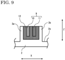
- FIG. 9 is a sectional view of the power conversion device 1 taken at a D-D cross-section position in FIG. 8 .
- the shape of the protrusion 3 is different from that in embodiment 1.
- the cooling surface 2a has a first protrusion 3a and a second protrusion 3b provided with an interval therebetween and protruding toward the DC connection member 9 side. At least a part of the opposed portion of the DC connection member 9 is located so as to be interposed between a side surface of the first protrusion 3a and a side surface of the second protrusion 3b, and is thermally connected to the side surface of the first protrusion 3a and the side surface of the second protrusion 3b.
- the DC connection member 9 is thermally connected to the side surface of the first protrusion 3a and the side surface of the second protrusion 3b via the insulation member 12.
- the DC connection member 9 is stacked in the second direction. However, without limitation thereto, the DC connection member 9 may be stacked in the third direction as in embodiment 1.
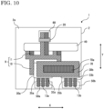
- FIG. 10 is a plan view schematically showing the power conversion device 1 according to embodiment 4
- FIG. 11 is another plan view schematically showing the power conversion device 1, with the control board 70 removed.
- the power conversion device 1 according to embodiment 4 includes two power modules.
- the power conversion device 1 includes a plurality of power modules, and the plurality of power modules are provided so as to be arranged in the second direction.
- the power conversion device 1 includes a first power module 30a and a second power module 30b, and the first power module 30a and the second power module 30b are provided so as to be arranged in the second direction.
- the first power module 30a has a first module body portion 35a, a first positive-side DC connection terminal 31a and a first negative-side DC connection terminal 32a which are DC connection terminals protruding from the first module body portion 35a and electrically connected to the DC connection member 9, and a first AC connection terminal 33a protruding from the first module body portion 35a and electrically connected to a first AC connection member 13a.
- the second power module 30b has a second module body portion 35b, a second positive-side DC connection terminal 31b and a second negative-side DC connection terminal 32b which are DC connection terminals protruding from the second module body portion 35b and electrically connected to the DC connection member 9, and a second AC connection terminal 33b protruding from the second module body portion 35b and electrically connected to the second AC connection member 13b. Arrangement of these terminals is the same as that of the terminals of the power module 30 shown in embodiment 1.
- the DC connection member 9 has the positive-side connection member 10 electrically connected to the positive-side terminal 41 of the capacitor 40, the first positive-side DC connection terminal 31a, and the second positive-side DC connection terminal 31b, and the negative-side connection member 11 electrically connected to the negative-side terminal 42 of the capacitor 40, the first negative-side DC connection terminal 32a, and the second negative-side DC connection terminal 32b.
- a first AC output portion 50a is located on the one side in the first direction of the first module body portion 35a.
- a second AC output portion 50b is located on the one side in the first direction of the second module body portion 35b.
- the DC input portion 60 is located on the other side in the first direction of the capacitor 40.
- the DC connection member 9 is connected to the battery 100 (not shown), at the DC input portion 60.
- the DC connection terminal and the AC connection terminal are separately provided in different directions, and therefore, even in a case where two or more power modules are provided, the power modules can be arranged in a row, whereby the size of the power conversion device 1 can be reduced.
- the capacitor 40 and each power module can be connected in the same manner as in embodiment 1, and therefore, even in a case where a plurality of power modules are provided, a complicated assembly process such as arranging the capacitor 40 or the power modules three-dimensionally is not needed, so that the same production process as in embodiment 1 can be used. Since the same production process as in embodiment 1 can be used, mixed-flow production with the power conversion device 1 of embodiment 1 can be performed.
- connection from the first AC connection terminal 33a to the first AC output portion 50a and connection from the second AC connection terminal 33b to the second AC output portion 50b can be made through the shortest distances, whereby component cost is reduced, the weights of components can be reduced, and radiation noise can be reduced.
- lengths of the DC connection member 9 between each DC connection terminal of the plurality of power modules and the power supply connection terminal portion 9a which is a part of the DC connection member 9 and is connected to the DC power supply are equivalent to each other.
- the length of the DC connection member 9 between the first positive-side DC connection terminal 31a and the power supply connection terminal portion 9a is equivalent to the length of the DC connection member 9 between the second positive-side DC connection terminal 31b and the power supply connection terminal portion 9a.
- the DC input portion 60 is located on the other side in the first direction between the first positive-side DC connection terminal 31a and the second positive-side DC connection terminal 31b.
- the control board 70 has one control operation unit 70a for controlling switching operations of power semiconductor elements that the plurality of power modules respectively have.
- the control operation unit 70a controls the first power module 30a and the second power module 30b.
- the power conversion device 1 according to the present embodiment is provided in a vehicle
- an application example for a series hybrid in which power is generated by an engine and the power is used for traveling of the vehicle or charging of a battery will be described.
- the protrusion 3 may be provided near a connection part of the DC connection member 9 with the capacitor 40 or at the positive-side terminal 41 and the negative-side terminal 42 of the capacitor 40, whereby thermal influence on the capacitor 40 can be reduced.
- the DC connection member 9 is located between the capacitor 40, and the first power module 30a and the second power module 30b.
- the location of the DC connection member 9 is not limited thereto.
- the DC input portion 60 may be located adjacently to the first AC output portion 50a, whereby the DC connection member 9 can be located on the side of the first AC output portion 50a and the second AC output portion 50b. In a case where the DC connection member 9 is located on the side of the first AC output portion 50a and the second AC output portion 50b, thermal influence on the capacitor 40 can be further reduced.
- a gap may be provided between the capacitor 40 and the cooling surface 2a, and the DC connection member 9 may be located in the gap.
- the DC connection member 9 can be efficiently cooled.
- the capacitor 40 can be located near the first power module 30a and the second power module 30b, so that heat generation at the power semiconductor elements 300 is reduced owing to inductance reduction of the DC connection member 9, whereby efficiency of the power conversion device 1 can be enhanced.
- FIG. 10 an example in which two power modules are provided is shown, but the number of power modules is not limited to two.
- the power conversion device 1 with three power modules provided to the power conversion device 1, front wheels and rear wheels can be controlled separately from each other. In this way, also in a case where an additional function is imparted to the power conversion device 1, the power conversion device 1 according to the present disclosure is effective.
- the power conversion device 1 according to the present embodiment is applied to an electric vehicle having a large-output motor, will be described.
- there is an upper limit on current that can flow through a power module and a plurality of power modules are needed for driving a large-output motor.
- Examples of large-output motors include a motor with six phases instead of three phases, and a motor having two sets of windings while having three phases.
- the length of the DC connection member 9 between the first positive-side DC connection terminal 31a and the power supply connection terminal portion 9a is equivalent to the length of the DC connection member 9 between the second positive-side DC connection terminal 31b and the power supply connection terminal portion 9a.
- power can be supplied to the first power module 30a and the second power module 30b with no delay therebetween, whereby the two power modules can be used in parallel. Since the two power modules can be used in parallel, it is possible to adapt to output increase for the two power modules, and thus it is possible to adapt also to a six-phase motor and a three-phase two-set inverter.
- the power conversion device 1 adapted to one small-output motor, two small-output motors, or one large-output motor can be manufactured with a similar component configuration and similar component arrangement.
- mixed-flow production can be performed on the same assembly line, whereby production efficiency of the power conversion device 1 can be improved.
- a power conversion device comprising:
- control board is located so as to overlap the power module without overlapping the positive-side connection member and the negative-side connection member, as seen in a direction perpendicular to the cooling surface.
- the power conversion device wherein at least a part of the opposed portion has a top surface opposed part opposed to a top surface of the protrusion and a side surface opposed part opposed to a side surface of the protrusion, and thus is bent so as to surround the protrusion.
- the power conversion device comprising a magnetic member provided at the cooling surface and surrounding the DC connection member, wherein the DC connection member is thermally connected to the cooling surface via the magnetic member.
- the power conversion device according to any one of additional notes 1 to 13, comprising a plurality of the power modules, wherein the plurality of power modules are provided so as to be arranged in the second direction.
- control board has one control operation unit for controlling switching operations of the power semiconductor elements that the plurality of power modules respectively have.
- the power conversion device according to any one of additional notes 1 to 16, wherein the power semiconductor element that the power module has is a wide bandgap semiconductor element.
- the power conversion device according to any one of additional notes 1 to 16, wherein the power semiconductor element that the power module has is an RC-IGBT having a switching element and a flyback diode integrated with each other.
Landscapes
- Engineering & Computer Science (AREA)
- Power Engineering (AREA)
- Microelectronics & Electronic Packaging (AREA)
- Life Sciences & Earth Sciences (AREA)
- Sustainable Development (AREA)
- Sustainable Energy (AREA)
- Transportation (AREA)
- Mechanical Engineering (AREA)
- Physics & Mathematics (AREA)
- Thermal Sciences (AREA)
- Inverter Devices (AREA)
Abstract
Description
- The present disclosure relates to a power conversion device.
- In an electrified vehicle such as an electric vehicle or a hybrid vehicle using a motor as a driving source, a power conversion device for electric powertrain is provided. Examples of power conversion devices include a charger which converts commercial AC power to DC power to charge a high-voltage battery, a DC/DC converter which converts DC power of a high-voltage battery to voltage (e.g., 12 V) for an auxiliary-device battery, and an inverter which converts DC power of a battery to AC power for a motor. The power conversion device is a device that converts input current from DC to AC or from AC to DC, or converts input voltage to different voltage.
- In such a power conversion device used in an electrified vehicle, size reduction of main circuit components such as a power module and a capacitor has been attempted in order to reduce a projected area. Meanwhile, when the sizes of a power module and a capacitor are reduced, the degree of freedom of directions in which wiring components of a main circuit for supplying power are led out is reduced, so that connection between wiring components and with the main circuit is complicated.
- A configuration of a vehicular power conversion device incorporating some measures using a power module structure so as to achieve inductance reduction and size reduction, is disclosed (see, for example, Patent Document 1). In the configuration disclosed in
Patent Document 1, a DC input portion and an AC output portion of a power module having a reduced size are arranged in an L shape. In addition, in order to connect the power module and a capacitor, a PN stacked busbar having a large area is provided above the power module. - Patent Document 1:
Japanese Laid-Open Patent Publication No. 2011-15460 - In
Patent Document 1, since the DC input portion and the AC output portion of the power module are arranged in an L shape, the size of the power module can be reduced. In addition, since the PN stacked busbar having a large area is provided above the power module, the inductance of the power conversion device can be reduced. However, in this structure, since PN terminals in the power module and the PN stacked busbar having a large area are provided above the power module, heat generated at the PN stacked busbar having an increased size influences members provided therearound. In addition, considering suppression of heat generation at the PN stacked busbar, the output of the power conversion device cannot be increased. - The present disclosure has been made to solve the above problems, and an object of the present disclosure is to provide a power conversion device having an increased output while suppressing heat generation at a DC connection member connecting a power module and a capacitor.
- A power conversion device according to the present disclosure includes: a DC connection member through which DC power flows; an AC connection member through which AC power flows; a power module electrically connected to the DC connection member and the AC connection member, and having a power semiconductor element for performing power conversion between the DC power of the DC connection member and the AC power of the AC connection member; a capacitor electrically connected to the DC connection member; a housing having a cooler and a cooling surface cooled by the cooler, the power module being thermally connected to the cooling surface; and a control board which controls a switching operation of the power semiconductor element. The power module has a module body portion, a DC connection terminal protruding from the module body portion and electrically connected to the DC connection member, and an AC connection terminal protruding from the module body portion and electrically connected to the AC connection member. One direction parallel to the cooling surface is defined as a first direction, and a direction parallel to the cooling surface and perpendicular to the first direction is defined as a second direction. The AC connection member and the AC connection terminal are located on one side in the first direction of the module body portion, and the capacitor is located on another side in the first direction of the module body portion. The DC connection terminal is located on one side or another side in the second direction of the module body portion. The DC connection member has an opposed portion opposed to the cooling surface, and at least a part of the opposed portion is thermally connected to the cooling surface.
- The power conversion device according to the present disclosure includes the power module electrically connected to the DC connection member, and the capacitor electrically connected to the DC connection member. The power module has the module body portion, the DC connection terminal protruding from the module body portion and electrically connected to the DC connection member, and the AC connection terminal protruding from the module body portion and electrically connected to the AC connection member. The AC connection member and the AC connection terminal are located on the one side in the first direction of the module body portion, and the capacitor is located on the other side in the first direction of the module body portion. The DC connection terminal is located on the one side or the other side in the second direction of the module body portion. The DC connection member has the opposed portion opposed to the cooling surface, and at least a part of the opposed portion is thermally connected to the cooling surface. Thus, heat generated at the DC connection member, heat transferred from the power module side to the DC connection member, and heat transferred from the capacitor side to the DC connection member, can be dissipated to the housing from the opposed portion thermally connected to the cooling surface. Thus, the power conversion device having an increased output while suppressing heat generation at the DC connection member can be provided.
-
- [
FIG. 1] FIG. 1 schematically shows a circuit of a power conversion device according toembodiment 1. - [
FIG. 2] FIG. 2 is a plan view schematically showing the power conversion device according toembodiment 1. - [
FIG. 3] FIG. 3 is a sectional view of the power conversion device taken at an A-A cross-section position inFIG. 2 . - [
FIG. 4] FIG. 4 is a sectional view of the power conversion device taken at a B-B cross-section position inFIG. 2 . - [
FIG. 5] FIG. 5 is a sectional view of the power conversion device taken at a C-C cross-section position inFIG. 2 . - [
FIG. 6] FIG. 6 is a sectional view showing a specific part of another power conversion device according toembodiment 1. - [
FIG. 7] FIG. 7 is a plan view schematically showing a power conversion device according toembodiment 2. - [
FIG. 8] FIG. 8 is a plan view schematically showing a power conversion device according toembodiment 3. - [
FIG. 9] FIG. 9 is a sectional view of the power conversion device taken at a D-D cross-section position inFIG. 8 . - [
FIG. 10] FIG. 10 is a plan view schematically showing a power conversion device according to embodiment 4. - [
FIG. 11] FIG. 11 is another plan view schematically showing the power conversion device according to embodiment 4. - Hereinafter, a power conversion device according to embodiments of the present disclosure will be described with reference the drawings. In the drawings, the same or corresponding members and parts are denoted by the same reference characters, to give description.
-
FIG. 1 schematically shows a circuit of apower conversion device 1 according toembodiment 1,FIG. 2 is a plan view schematically showing thepower conversion device 1,FIG. 3 is a sectional view of thepower conversion device 1 taken at an A-A cross-section position inFIG. 2 ,FIG. 4 is a sectional view of thepower conversion device 1 taken at a B-B cross-section position inFIG. 2 , andFIG. 5 is a sectional view of thepower conversion device 1 taken at a C-C cross-section position inFIG. 2 . Thepower conversion device 1 is a device that converts input current from DC to AC or from AC to DC, or converts input voltage to different voltage. In the present disclosure, thepower conversion device 1 is described as a three-phase inverter that converts DC power to AC power, but the power conversion device according to the present disclosure is not limited to a three-phase inverter. - The schematic circuit configuration of the
power conversion device 1 will be described with reference toFIG. 1 . Thepower conversion device 1 includes apower module 30 and acapacitor 40. Thepower conversion device 1 is connected to abattery 100 present outside. Thepower conversion device 1 includes aDC connection member 9 through which DC power flows, and anAC connection member 13 through which AC power flows. Thecapacitor 40 is electrically connected to theDC connection member 9. Thepower module 30 is electrically connected to theDC connection member 9 and theAC connection member 13. Thepower module 30 has a plurality ofpower semiconductor elements 300 for performing power conversion between DC power of theDC connection member 9 and AC power of theAC connection member 13. The AC power is outputted from theAC connection member 13 to a three-phase motor 101, thus driving the three-phase motor 101. - As the
power semiconductor elements 300, a power control semiconductor element such as a metal oxide semiconductor field effect transistor (MOSFET) or an insulated gate bipolar transistor (IGBT), a flyback diode, or the like is used. The semiconductor elements are not limited thereto, and another semiconductor element such as a bipolar transistor may be used. In the present embodiment, a configuration in which a MOSFET is used and a parasitic diode of the MOSFET is used as a flyback diode, is adopted. However, for example, in such a case where a switching element such as an IGBT that does not have a parasitic diode is used, a flyback diode may be added in parallel. Alternatively, a reverse conducting IGBT (RC-IGBT) having a switching element and a flyback diode integrated with each other may be used. - In a case where a MOSFET or an RC-IGBT is used for the
power semiconductor elements 300, it becomes unnecessary to provide a flyback diode, so that the number of elements provided in thepower module 30 is decreased, whereby the size of thepower module 30 can be reduced. Since the size of thepower module 30 is reduced, the space for providing thecapacitor 40 can be easily ensured, and therefore the space for cooling theDC connection member 9 can be easily ensured. - The
power semiconductor elements 300 are formed at a semiconductor substrate made of a material such as silicon, silicon carbide, or gallium nitride, and a wide bandgap semiconductor element having a wider bandgap than silicon may be used for thepower semiconductor elements 300. In a case where a MOSFET made of silicon carbide, which is a wide bandgap semiconductor element, is used, a temporal change di/dt of current occurring in switching can be made greater than in a case of a MOSFET made of silicon. In addition, since the wide bandgap semiconductor element is small in ON resistance, small in loss, and small in heat generation, the chip area can be reduced. Since the chip area is reduced, the size of thepower module 30 can be reduced. Since the size of thepower module 30 is reduced, the space for providing thecapacitor 40 can be easily ensured, and therefore the space for cooling theDC connection member 9 can be easily ensured. - The configuration of the
power conversion device 1 will be described with reference toFIG. 2 to FIG. 5 . Thepower conversion device 1 includes thepower module 30, thecapacitor 40, theDC connection member 9, theAC connection member 13, ahousing 2, and acontrol board 70. Thepower conversion device 1 further includes aDC input portion 60 which is a part where theDC connection member 9 is connected to thebattery 100, anAC output portion 50 which is a part where theAC connection member 13 is connected to the three-phase motor 101, and amagnetic member 20. Thehousing 2 has a cooler 4 and acooling surface 2a cooled by the cooler 4. Thepower module 30 is thermally connected to thecooling surface 2a. Thecontrol board 70 controls switching operations of thepower semiconductor elements 300. In the drawings, one direction parallel to thecooling surface 2a is defined as a first direction (arrow Y), a direction parallel to thecooling surface 2a and perpendicular to the first direction is defined as a second direction (arrow X), and a direction perpendicular to the first direction and the second direction is defined as a third direction (arrow Z). - The
housing 2 is made from a metal material such as aluminum, or a resin member. The cooler 4 is a flow path through which a coolant flows, for example. As the coolant, for example, water or an ethylene glycol solution is used. InFIG. 3 , a configuration in which the cooler 4 is provided in thehousing 2 is shown. However, without limitation thereto, the cooler 4 may be provided at a surface of thehousing 2 on a side opposite to thecooling surface 2a. Such a cooler 4 may be further provided on thecapacitor 40 side. In the present embodiment, in addition to thepower module 30, thecapacitor 40 is thermally connected to thecooling surface 2a. With this configuration, heat generated at thecapacitor 40 is transferred to thehousing 2, whereby temperature increase in thecapacitor 40 can be suppressed. Since temperature increase in thecapacitor 40 is suppressed, the life of thecapacitor 40 can be prolonged. - In the present embodiment, a positive-
side terminal 41 and a negative-side terminal 42 of thecapacitor 40 are formed such that terminal parts made of metal are coated with a resin member. The positive-side terminal 41 and the negative-side terminal 42 are parts indicated by broken lines inFIG. 2 . The positive-side terminal 41 and the negative-side terminal 42 are thermally connected to thehousing 2 via resin member parts. Thus, heat generated at thecapacitor 40 can be dissipated to thehousing 2 through the positive-side terminal 41 and the negative-side terminal 42. Since heat generated at thecapacitor 40 is dissipated to thehousing 2 through the positive-side terminal 41 and the negative-side terminal 42, temperature increase in thecapacitor 40 can be further suppressed, whereby the life of thecapacitor 40 can be further prolonged. In the present embodiment, thecapacitor 40, the positive-side terminal 41, and the negative-side terminal 42 are directly provided at thecooling surface 2a. However, a heat dissipation member may be provided between the above member and thecooling surface 2a. - As shown in
FIG. 3 , thepower module 30 has amodule body portion 35, a positive-sideDC connection terminal 31 and a negative-sideDC connection terminal 32 which are DC connection terminals protruding from themodule body portion 35 and electrically connected to theDC connection member 9, anAC connection terminal 33 protruding from themodule body portion 35 and electrically connected to theAC connection member 13, and asignal terminal 34 protruding from themodule body portion 35 and electrically connected to thecontrol board 70. TheDC connection member 9 has a positive-side connection member 10 electrically connected to the positive-side terminal 41 of thecapacitor 40 and the positive-sideDC connection terminal 31, and a negative-side connection member 11 electrically connected to the negative-side terminal 42 of thecapacitor 40 and the negative-sideDC connection terminal 32. - The arrangement configuration of portions composing the
power conversion device 1 and the details of the configuration will be described. As shown inFIG. 2 , theAC connection member 13 and theAC connection terminal 33 are located on one side in the first direction of themodule body portion 35, and thecapacitor 40 is located on another side in the first direction of themodule body portion 35. The positive-sideDC connection terminal 31 and the negative-sideDC connection terminal 32 are located on one side or another side in the second direction of themodule body portion 35. In the present embodiment, the positive-sideDC connection terminal 31 and the negative-sideDC connection terminal 32 are located on the one side in the second direction of themodule body portion 35. With this configuration, the DC connection terminal and theAC connection terminal 33 are separately provided in different directions, whereby the size of thepower module 30 can be reduced. - The
DC connection member 9 has an opposed portion opposed to thecooling surface 2a, and at least a part of the opposed portion is thermally connected to thecooling surface 2a. With this configuration, heat generated at theDC connection member 9, heat transferred from thepower module 30 side to theDC connection member 9, and heat transferred from thecapacitor 40 side to theDC connection member 9, can be dissipated to thehousing 2 from the opposed portion thermally connected to thecooling surface 2a. Thus, thepower conversion device 1 having an increased output while suppressing heat generation at theDC connection member 9 can be provided. In the present embodiment, as shown inFIG. 3 , the coolingsurface 2a has aprotrusion 3 protruding toward theDC connection member 9 side, and at least a part of the opposed portion is thermally connected to theprotrusion 3. With this configuration, heat generated at theDC connection member 9, heat transferred from the positive-sideDC connection terminal 31 and the negative-sideDC connection terminal 32 to theDC connection member 9, and heat transferred from the positive-side terminal 41 and the negative-side terminal 42 to theDC connection member 9, can be dissipated to thehousing 2 through theprotrusion 3. Since heat of theDC connection member 9 is dissipated to thehousing 2 through theprotrusion 3, temperature increase in thecapacitor 40 can be suppressed even when large current flows, whereby the life of thecapacitor 40 can be prolonged. - An
insulation member 12 or anadditional insulation member 12a is provided between theDC connection member 9 and theprotrusion 3, thus making insulation between theDC connection member 9 and theprotrusion 3. InFIG. 3 , an example in which theinsulation member 12 and theadditional insulation member 12a formed in sheet shapes are provided, is shown. However, the configurations of theinsulation member 12 and theadditional insulation member 12a are not limited thereto, and theinsulation member 12 may be air or may be a liquid or solid insulation member. - In the present embodiment, a configuration in which the opposed portion is thermally connected to the
protrusion 3 is shown. However, a configuration for thermally connecting the opposed portion to thecooling surface 2a is not limited thereto. TheDC connection member 9 may be bent to thecooling surface 2a side so that the opposed portion is thermally connected to thecooling surface 2a. In a case where theprotrusion 3 is provided and the opposed portion is thermally connected to theprotrusion 3, the length of theDC connection member 9 can be shortened, whereby the inductance of theDC connection member 9 can be reduced. Since the inductance of theDC connection member 9 is reduced, heat generation at theDC connection member 9 can be suppressed. - The positive-
side connection member 10 and the negative-side connection member 11 are located on the one side or the other side in the second direction of themodule body portion 35. In the present embodiment, the positive-side connection member 10 and the negative-side connection member 11 are located on the one side in the second direction of themodule body portion 35. With this configuration, the positive-side connection member 10 and the negative-side connection member 11 do not pass on thecontrol board 70 side of themodule body portion 35, and therefore heat of theDC connection member 9 can be efficiently dissipated to thehousing 2. In addition, the length of theDC connection member 9 can be shortened, whereby the inductance of theDC connection member 9 can be reduced. In addition, since the positive-side connection member 10 and the negative-side connection member 11 do not pass on thecontrol board 70 side of themodule body portion 35, thepower conversion device 1 can be formed with a small height. - In the present embodiment, the
control board 70 is located so as to overlap thepower module 30 without overlapping the positive-side connection member 10 and the negative-side connection member 11, as seen in the direction perpendicular to thecooling surface 2a, as shown inFIG. 2 . With this configuration, the positive-side connection member 10 and the negative-side connection member 11 are not located on one side or another side in the third direction of thecontrol board 70, and therefore the positive-side connection member 10 and the negative-side connection member 11 are not present near thecontrol board 70. Thus, heat transfer and noise influence from the positive-side connection member 10 and the negative-side connection member 11 to thecontrol board 70 can be reduced. - In the present embodiment, the positive-
side connection member 10 and the negative-side connection member 11 are each formed in a plate shape. The positive-side connection member 10 and the negative-side connection member 11 are made from a metal material such as copper, for example. As shown inFIG. 3 , the positive-side connection member 10 and the negative-side connection member 11 have parts arranged in a stacked manner with theinsulation member 12 interposed therebetween. With this configuration, the positive-side connection member 10 and the negative-side connection member 11 are arranged so as to form parallel flat plates, whereby the inductance of theDC connection member 9 can be reduced. Since the inductance of theDC connection member 9 is reduced, surge voltage due to switching of thepower semiconductor elements 300 can be reduced. - In the present embodiment, as shown in
FIG. 2 , theDC connection member 9 is branched at a part between thecapacitor 40 and the DC connection terminal. A branched connection member which is a branched part of theDC connection member 9 has, at an end on a side opposite to a branch-base side, a power supplyconnection terminal portion 9a connected to a DC power supply. The power supplyconnection terminal portion 9a is connected to the battery 100 (not shown inFIG. 2 ) which is the DC power supply, at theDC input portion 60. With this configuration, even in a case where large current is sent or received to or from the DC side, e.g., power is supplied from theDC input portion 60 to another power module or load, since at least a part of the opposed portion of theDC connection member 9 is thermally connected to thecooling surface 2a, temperature increase in thecapacitor 40 can be suppressed and a long life of thecapacitor 40 can be ensured. - The
DC input portion 60 and theAC output portion 50 are located at different positions. TheAC output portion 50 is located on the one side in the first direction of themodule body portion 35, as with theAC connection member 13 and theAC connection terminal 33. TheDC input portion 60 is located on the one side in the second direction of themodule body portion 35, as with the positive-sideDC connection terminal 31 and the negative-sideDC connection terminal 32. Owing to the above arrangement of theDC input portion 60 and theAC output portion 50, in a case where the three-phase motor 101 and thepower conversion device 1 are integrated with each other, if the position of theAC output portion 50 is at a motor-axis-direction end which can be easily connected with the three-phase motor 101, thebattery 100 is located in a direction (DC input portion 60 side) different from the motor-axis direction, so that thebattery 100 and theDC input portion 60 can be easily connected. - In the present embodiment, as shown in
FIG. 4 , at least a part of the opposed portion of theDC connection member 9 has a top surface opposedpart 9b opposed to a top surface of theprotrusion 3 and a side surface opposedpart 9c opposed to a side surface of theprotrusion 3, and thus is bent so as to surround theprotrusion 3. With this configuration, the area of the opposed portion of theDC connection member 9 thermally connected to theprotrusion 3 can be increased, whereby the effect of heat dissipation from theDC connection member 9 to thehousing 2 can be enhanced. In addition, the sectional areas of the positive-side connection member 10 and the negative-side connection member 11 composing theDC connection member 9 are increased and their resistance values are decreased, whereby the positive-side connection member 10 and the negative-side connection member 11 can adapt to large current. In addition, by reducing the thicknesses of the positive-side connection member 10 and the negative-side connection member 11, the cost and the weight can be reduced. - In
FIG. 4 , an example in which the top surface opposedparts 9b and the side surface opposedparts 9c are provided at a part where the positive-side connection member 10 and the negative-side connection member 11 are arranged without being stacked, is shown. However, the present disclosure is not limited thereto. The top surface opposedparts 9b and the side surface opposedparts 9c may be provided at a part where the positive-side connection member 10 and the negative-side connection member 11 are arranged in a stacked manner. In a case where the positive-side connection member 10 and the negative-side connection member 11 are arranged in a stacked manner, the top surface opposedpart 9b of one connection member may have a cutout for the purpose of screwing the other connection member. In a case where the top surface opposedpart 9b and the side surface opposedpart 9c are provided at a part where the positive-side connection member 10 and the negative-side connection member 11 are arranged in a stacked manner, even if the top surface opposedpart 9b of one connection member has a cutout for the purpose of screwing the other connection member, current flowing through the top surface opposedpart 9b which has a cutout and thus is not a parallel flat plate is reduced but current flows through the side surface opposedpart 9c which is a parallel flat plate. Thus, reduced inductances of the positive-side connection member 10 and the negative-side connection member 11 can be maintained and a sectional area needed for current conduction can be ensured. - In the present embodiment, as shown in
FIG. 5 , theadditional insulation member 12a is provided between theprotrusion 3 and theDC connection member 9 thermally connected to theprotrusion 3, and theadditional insulation member 12a is integrated with theinsulation member 12 on a side of one side surface of theDC connection member 9 thermally connected to theprotrusion 3. InFIG. 5 , theDC connection member 9 thermally connected to theprotrusion 3 is the negative-side connection member 11. One insulation member is bent at a side surface part of the negative-side connection member 11, thus forming theinsulation member 12 and theadditional insulation member 12a. With this configuration, both insulation parts between the positive-side connection member 10 and the negative-side connection member 11 and between the negative-side connection member 11 and theprotrusion 3 can be formed by one insulation member, whereby component cost and working cost for the insulation member can be reduced. In addition, since theinsulation member 12 contacting with the positive-side connection member 10 contacts with thehousing 2, the effect of heat dissipation from the positive-side connection member 10 to thehousing 2 can be enhanced. - In the present embodiment, the
power conversion device 1 includes themagnetic member 20 provided at thecooling surface 2a and surrounding theDC connection member 9. Themagnetic member 20 is a member for suppressing noise. TheDC connection member 9 is thermally connected to thecooling surface 2a via themagnetic member 20. With this configuration, even at a part where theprotrusion 3 is not provided, theDC connection member 9 can be easily thermally connected to thecooling surface 2a without changing the length of theDC connection member 9. Although the negative-side connection member 11 is shown inFIG. 5 , the positive-side connection member 10 is also surrounded by themagnetic member 20 in the same manner, and thus the positive-side connection member 10 is also thermally connected to thecooling surface 2a. In addition, theinsulation member 12 may be provided between theDC connection member 9 and themagnetic member 20. - In
FIG. 5 , an example in which themagnetic member 20 is provided at a part where the positive-side connection member 10 and the negative-side connection member 11 are arranged without being stacked, is shown. However, the present disclosure is not limited thereto. As shown inFIG. 6 , themagnetic member 20 may be provided at a part where the positive-side connection member 10 and the negative-side connection member 11 are arranged in a stacked manner.FIG. 6 is a sectional view showing a specific part of anotherpower conversion device 1 according toembodiment 1, taken at themagnetic member 20 part. InFIG. 6 , theadditional insulation member 12a is provided between themagnetic member 20 and theDC connection member 9 thermally connected to themagnetic member 20, and theadditional insulation member 12a is integrated with theinsulation member 12 on a side of one side surface of theDC connection member 9 thermally connected to themagnetic member 20. InFIG. 6 , theDC connection member 9 thermally connected to themagnetic member 20 is the negative-side connection member 11. One insulation member is bent at a side surface part of the negative-side connection member 11, thus forming theinsulation member 12 and theadditional insulation member 12a. With this configuration, both insulation parts between the positive-side connection member 10 and the negative-side connection member 11 and between the negative-side connection member 11 and themagnetic member 20 can be formed by one insulation member, whereby component cost and working cost for the insulation member can be reduced. In addition, since theinsulation member 12 contacting with the positive-side connection member 10 contacts with themagnetic member 20, the effect of heat dissipation from the positive-side connection member 10 to themagnetic member 20 can be enhanced. - As described above, the
power conversion device 1 according toembodiment 1 includes thepower module 30 electrically connected to theDC connection member 9, and thecapacitor 40 electrically connected to theDC connection member 9. Thepower module 30 has themodule body portion 35, the DC connection terminal protruding from themodule body portion 35 and electrically connected to theDC connection member 9, and theAC connection terminal 33 protruding from themodule body portion 35 and electrically connected to theAC connection member 13. TheAC connection member 13 and theAC connection terminal 33 are located on the one side in the first direction of themodule body portion 35, and thecapacitor 40 is located on the other side in the first direction of themodule body portion 35. The DC connection terminal is located on the one side or the other side in the second direction of themodule body portion 35. TheDC connection member 9 has the opposed portion opposed to thecooling surface 2a, and at least a part of the opposed portion is thermally connected to thecooling surface 2a. Thus, heat generated at theDC connection member 9, heat transferred from thepower module 30 side to theDC connection member 9, and heat transferred from thecapacitor 40 side to theDC connection member 9, can be dissipated to thehousing 2 from the opposed portion thermally connected to thecooling surface 2a. Thus, thepower conversion device 1 having an increased output while suppressing heat generation at theDC connection member 9 can be provided. - The DC connection terminal may have the positive-side
DC connection terminal 31 and the negative-sideDC connection terminal 32. TheDC connection member 9 may have the positive-side connection member 10 electrically connected to the positive-side terminal 41 of thecapacitor 40 and the positive-sideDC connection terminal 31, and the negative-side connection member 11 electrically connected to the negative-side terminal 42 of thecapacitor 40 and the negative-sideDC connection terminal 32. The positive-side connection member 10 and the negative-side connection member 11 may be located on the one side or the other side in the second direction of themodule body portion 35. Thus, the positive-side connection member 10 and the negative-side connection member 11 do not pass on thecontrol board 70 side of themodule body portion 35, and therefore heat of theDC connection member 9 can be efficiently dissipated to thehousing 2. In addition, the length of theDC connection member 9 can be shortened, whereby the inductance of theDC connection member 9 can be reduced. - The
control board 70 may be located so as to overlap the power module without overlapping the positive-side connection member 10 and the negative-side connection member 11, as seen in the direction perpendicular to thecooling surface 2a. Thus, the positive-side connection member 10 and the negative-side connection member 11 are not located on the one side or the other side in the third direction of thecontrol board 70, and therefore heat transfer and noise influence from the positive-side connection member 10 and the negative-side connection member 11 to thecontrol board 70 can be reduced. The positive-side connection member 10 and the negative-side connection member 11 may be each formed in a plate shape, and the positive-side connection member 10 and the negative-side connection member 11 may have parts arranged in a stacked manner with theinsulation member 12 interposed therebetween. Thus, the positive-side connection member 10 and the negative-side connection member 11 are arranged so as to form parallel flat plates, whereby the inductance of theDC connection member 9 can be reduced. - The cooling
surface 2a may have theprotrusion 3 protruding toward theDC connection member 9 side, and at least a part of the opposed portion may be thermally connected to theprotrusion 3. Thus, heat generated at theDC connection member 9, heat transferred from the positive-sideDC connection terminal 31 and the negative-sideDC connection terminal 32 to theDC connection member 9, and heat transferred from the positive-side terminal 41 and the negative-side terminal 42 to theDC connection member 9, can be easily dissipated to thehousing 2 through theprotrusion 3. In addition, in a case where theprotrusion 3 is provided and the opposed portion is thermally connected to theprotrusion 3, the length of theDC connection member 9 can be shortened, whereby the inductance of theDC connection member 9 can be reduced. - At least a part of the opposed portion may have the top surface opposed
part 9b opposed to the top surface of theprotrusion 3, and the side surface opposedpart 9c opposed to the side surface of theprotrusion 3, and thus may be bent so as to surround theprotrusion 3. Thus, the area of the opposed portion of theDC connection member 9 thermally connected to theprotrusion 3 can be increased, whereby the effect of heat dissipation from theDC connection member 9 to thehousing 2 can be enhanced. Theadditional insulation member 12a may be provided between theprotrusion 3 and theDC connection member 9 thermally connected to theprotrusion 3, and theadditional insulation member 12a may be integrated with theinsulation member 12 on a side of one side surface of theDC connection member 9 thermally connected to theprotrusion 3. Thus, both insulation parts between the positive-side connection member 10 and the negative-side connection member 11 and between the negative-side connection member 11 and theprotrusion 3 can be formed by one insulation member, whereby component cost and working cost for the insulation member can be reduced. - The power conversion device may include the
magnetic member 20 provided at thecooling surface 2a and surrounding theDC connection member 9, and theDC connection member 9 may be thermally connected to thecooling surface 2a via themagnetic member 20. Thus, even at a part where theprotrusion 3 is not provided, theDC connection member 9 can be easily thermally connected to thecooling surface 2a without changing the length of theDC connection member 9. Theadditional insulation member 12a may be provided between themagnetic member 20 and theDC connection member 9 thermally connected to themagnetic member 20, and theadditional insulation member 12a may be integrated with theinsulation member 12 on a side of one side surface of theDC connection member 9 thermally connected to themagnetic member 20. Thus, both insulation parts between the positive-side connection member 10 and the negative-side connection member 11 and between the negative-side connection member 11 and themagnetic member 20 can be formed by one insulation member, whereby component cost and working cost for the insulation member can be reduced. - The
capacitor 40 may be thermally connected to thecooling surface 2a. Thus, heat generated at thecapacitor 40 is transferred to thehousing 2, whereby temperature increase in thecapacitor 40 can be suppressed. TheDC connection member 9 may be branched at a part between thecapacitor 40 and the DC connection terminal, and the branched connection member which is a branched part of the DC connection member may have, at an end on a side opposite to a branch-base side, the power supplyconnection terminal portion 9a connected to the DC power supply. Thus, even in a case where the power supplyconnection terminal portion 9a is connected to thebattery 100 which is the DC power supply, at theDC input portion 60, and large current is sent or received to or from the DC side, e.g., power is supplied from theDC input portion 60 to another power module or load, since at least a part of the opposed portion of theDC connection member 9 is thermally connected to thecooling surface 2a, temperature increase in thecapacitor 40 can be suppressed and a long life of thecapacitor 40 can be ensured. - The
power semiconductor element 300 that thepower module 30 has may be a wide bandgap semiconductor element. Thus, since the wide bandgap semiconductor element is small in ON resistance, small in loss, and small in heat generation, the chip area can be reduced, whereby the size of thepower module 30 can be reduced. Thepower semiconductor element 300 that thepower module 30 has may be an RC-IGBT having a switching element and a flyback diode integrated with each other. Thus, it becomes unnecessary to provide a flyback diode, so that the number of elements provided in thepower module 30 is decreased, whereby the size of thepower module 30 can be reduced. - A
power conversion device 1 according toembodiment 2 will be described.FIG. 7 is a plan view schematically showing thepower conversion device 1 according toembodiment 2. In thepower conversion device 1 according toembodiment 2, the shape of theDC connection member 9 and the location of theDC input portion 60 are different from those inembodiment 1. - The
DC connection member 9 extends from the positive-sideDC connection terminal 31 and the negative-sideDC connection terminal 32 which are DC connection terminals, toward the one side in the first direction of themodule body portion 35 and the other side in the first direction of themodule body portion 35. TheDC connection member 9 is connected to thecapacitor 40, at a part extending toward the other side in the first direction of themodule body portion 35. TheDC connection member 9 has, at an end on the one side in the first direction, the power supplyconnection terminal portion 9a connected to the DC power supply. The power supplyconnection terminal portion 9a is connected to thebattery 100 which is the DC power supply, at theDC input portion 60. TheDC input portion 60 is located on the one side in the first direction of themodule body portion 35, as with theAC output portion 50, so as to be adjacent to theAC output portion 50. The negative-side connection member 11 is formed to be, for example, partially bent, so as not to contact with the positive-sideDC connection terminal 31. - Since the power supply
connection terminal portion 9a is located on the one side in the first direction of theDC connection member 9 and theDC input portion 60 is located on the one side in the first direction of themodule body portion 35, theDC input portion 60 and theAC output portion 50 are located on the one side in the first direction of themodule body portion 35. Thus, when thepower conversion device 1 is provided in a vehicle, connections between thepower conversion device 1, and thebattery 100 and the three-phase motor 101, can be performed from the same direction, whereby assemblability of thepower conversion device 1 can be improved. In addition, shock-proofness which is particularly important for a high-voltage product provided in a vehicle can be ensured by only a measure for one location on the one side in the first direction of themodule body portion 35. In addition, since the length in the first direction of theDC connection member 9 increases, the opposed portion is enlarged, so that heat is further transferred from theDC connection member 9 to thehousing 2, whereby heat transfer from theDC connection member 9 to thecapacitor 40 can be reduced. Since heat transfer from theDC connection member 9 to thecapacitor 40 is reduced and thus temperature increase in thecapacitor 40 is suppressed, the life of thecapacitor 40 can be prolonged. - A
power conversion device 1 according toembodiment 3 will be described.FIG. 8 is a plan view schematically showing thepower conversion device 1 according toembodiment 3, andFIG. 9 is a sectional view of thepower conversion device 1 taken at a D-D cross-section position inFIG. 8 . In thepower conversion device 1 according toembodiment 3, the shape of theprotrusion 3 is different from that inembodiment 1. - The cooling
surface 2a has afirst protrusion 3a and asecond protrusion 3b provided with an interval therebetween and protruding toward theDC connection member 9 side. At least a part of the opposed portion of theDC connection member 9 is located so as to be interposed between a side surface of thefirst protrusion 3a and a side surface of thesecond protrusion 3b, and is thermally connected to the side surface of thefirst protrusion 3a and the side surface of thesecond protrusion 3b. In the present embodiment, theDC connection member 9 is thermally connected to the side surface of thefirst protrusion 3a and the side surface of thesecond protrusion 3b via theinsulation member 12. In the present embodiment, theDC connection member 9 is stacked in the second direction. However, without limitation thereto, theDC connection member 9 may be stacked in the third direction as inembodiment 1. - With this configuration, since the
DC connection member 9 is interposed between the side surface of thefirst protrusion 3a and the side surface of thesecond protrusion 3b, heat dissipation performance from theDC connection member 9 to thehousing 2 can be enhanced. Since heat transfer from theDC connection member 9 to thehousing 2 is promoted, heat transfer from theDC connection member 9 to thecapacitor 40 can be reduced. Since heat transfer from theDC connection member 9 to thecapacitor 40 is reduced and thus temperature increase in thecapacitor 40 is suppressed, the life of thecapacitor 40 can be prolonged. - A
power conversion device 1 according to embodiment 4 will be described.FIG. 10 is a plan view schematically showing thepower conversion device 1 according to embodiment 4, andFIG. 11 is another plan view schematically showing thepower conversion device 1, with thecontrol board 70 removed. Thepower conversion device 1 according to embodiment 4 includes two power modules. - The
power conversion device 1 includes a plurality of power modules, and the plurality of power modules are provided so as to be arranged in the second direction. In the present embodiment, thepower conversion device 1 includes afirst power module 30a and asecond power module 30b, and thefirst power module 30a and thesecond power module 30b are provided so as to be arranged in the second direction. - As shown in
FIG. 11 , thefirst power module 30a has a firstmodule body portion 35a, a first positive-sideDC connection terminal 31a and a first negative-sideDC connection terminal 32a which are DC connection terminals protruding from the firstmodule body portion 35a and electrically connected to theDC connection member 9, and a firstAC connection terminal 33a protruding from the firstmodule body portion 35a and electrically connected to a firstAC connection member 13a. Thesecond power module 30b has a secondmodule body portion 35b, a second positive-sideDC connection terminal 31b and a second negative-sideDC connection terminal 32b which are DC connection terminals protruding from the secondmodule body portion 35b and electrically connected to theDC connection member 9, and a secondAC connection terminal 33b protruding from the secondmodule body portion 35b and electrically connected to the secondAC connection member 13b. Arrangement of these terminals is the same as that of the terminals of thepower module 30 shown inembodiment 1. - The
DC connection member 9 has the positive-side connection member 10 electrically connected to the positive-side terminal 41 of thecapacitor 40, the first positive-sideDC connection terminal 31a, and the second positive-sideDC connection terminal 31b, and the negative-side connection member 11 electrically connected to the negative-side terminal 42 of thecapacitor 40, the first negative-sideDC connection terminal 32a, and the second negative-sideDC connection terminal 32b. A firstAC output portion 50a is located on the one side in the first direction of the firstmodule body portion 35a. A secondAC output portion 50b is located on the one side in the first direction of the secondmodule body portion 35b. TheDC input portion 60 is located on the other side in the first direction of thecapacitor 40. TheDC connection member 9 is connected to the battery 100 (not shown), at theDC input portion 60. - With this configuration, the DC connection terminal and the AC connection terminal are separately provided in different directions, and therefore, even in a case where two or more power modules are provided, the power modules can be arranged in a row, whereby the size of the
power conversion device 1 can be reduced. In addition, thecapacitor 40 and each power module can be connected in the same manner as inembodiment 1, and therefore, even in a case where a plurality of power modules are provided, a complicated assembly process such as arranging thecapacitor 40 or the power modules three-dimensionally is not needed, so that the same production process as inembodiment 1 can be used. Since the same production process as inembodiment 1 can be used, mixed-flow production with thepower conversion device 1 ofembodiment 1 can be performed. In addition, connection from the firstAC connection terminal 33a to the firstAC output portion 50a and connection from the secondAC connection terminal 33b to the secondAC output portion 50b can be made through the shortest distances, whereby component cost is reduced, the weights of components can be reduced, and radiation noise can be reduced. - In the present embodiment, lengths of the
DC connection member 9 between each DC connection terminal of the plurality of power modules and the power supplyconnection terminal portion 9a which is a part of theDC connection member 9 and is connected to the DC power supply, are equivalent to each other. InFIG. 11 , the length of theDC connection member 9 between the first positive-sideDC connection terminal 31a and the power supplyconnection terminal portion 9a is equivalent to the length of theDC connection member 9 between the second positive-sideDC connection terminal 31b and the power supplyconnection terminal portion 9a. Being equivalent means that the difference between compared lengths is within 10%. In the present embodiment, theDC input portion 60 is located on the other side in the first direction between the first positive-sideDC connection terminal 31a and the second positive-sideDC connection terminal 31b. With this configuration, power can be supplied to thefirst power module 30a and thesecond power module 30b with no delay therebetween, whereby the two power modules can be used in parallel. Since the two power modules can be used in parallel, it is possible to adapt to output increase for the two power modules, and thus it is possible to adapt also to a six-phase motor. - In the present embodiment, as shown in
FIG. 10 , thecontrol board 70 has onecontrol operation unit 70a for controlling switching operations of power semiconductor elements that the plurality of power modules respectively have. InFIG. 10 , thecontrol operation unit 70a controls thefirst power module 30a and thesecond power module 30b. With this configuration, the plurality of power modules are controlled by onecontrol operation unit 70a, and thus synchronous control or phase difference control for the plurality of power modules can be easily performed. - Regarding a case where the
power conversion device 1 according to the present embodiment is provided in a vehicle, an application example for a series hybrid in which power is generated by an engine and the power is used for traveling of the vehicle or charging of a battery, will be described. - In a case where the remaining battery amount is sufficiently large, power of the
battery 100 is supplied through theDC input portion 60 to thefirst power module 30a or thesecond power module 30b for traveling, so that the vehicle travels. At this time, DC current is maximized between theDC input portion 60 and the part from which theDC connection member 9 is branched to theDC input portion 60. In the arrangement shown inFIG. 10 , the part where DC current is maximized is away from the positive-side terminal 41 and the negative-side terminal 42 of thecapacitor 40, and therefore thermal influence on thecapacitor 40 is extremely small. - In a case where the remaining battery amount is small, power is supplied from the power module for power generation (the other one different from the power module for traveling) through the
DC connection member 9 to the power module for traveling, so that the vehicle travels. In addition, power is supplied through theDC connection member 9, to charge thebattery 100. At this time, DC current is maximized between the power module for power generation and the part from which theDC connection member 9 is branched to theDC input portion 60. In the arrangement shown inFIG. 11 , theprotrusion 3 may be provided near a connection part of theDC connection member 9 with thecapacitor 40 or at the positive-side terminal 41 and the negative-side terminal 42 of thecapacitor 40, whereby thermal influence on thecapacitor 40 can be reduced. - In
FIG. 11 , theDC connection member 9 is located between thecapacitor 40, and thefirst power module 30a and thesecond power module 30b. However, the location of theDC connection member 9 is not limited thereto. For example, theDC input portion 60 may be located adjacently to the firstAC output portion 50a, whereby theDC connection member 9 can be located on the side of the firstAC output portion 50a and the secondAC output portion 50b. In a case where theDC connection member 9 is located on the side of the firstAC output portion 50a and the secondAC output portion 50b, thermal influence on thecapacitor 40 can be further reduced. - A gap may be provided between the
capacitor 40 and thecooling surface 2a, and theDC connection member 9 may be located in the gap. In a case where theDC connection member 9 is located in a gap between thecapacitor 40 and thecooling surface 2a, theDC connection member 9 can be efficiently cooled. In addition, thecapacitor 40 can be located near thefirst power module 30a and thesecond power module 30b, so that heat generation at thepower semiconductor elements 300 is reduced owing to inductance reduction of theDC connection member 9, whereby efficiency of thepower conversion device 1 can be enhanced. - In
FIG. 10 , an example in which two power modules are provided is shown, but the number of power modules is not limited to two. For example, with three power modules provided to thepower conversion device 1, front wheels and rear wheels can be controlled separately from each other. In this way, also in a case where an additional function is imparted to thepower conversion device 1, thepower conversion device 1 according to the present disclosure is effective. - An example in which the
power conversion device 1 according to the present embodiment is applied to an electric vehicle having a large-output motor, will be described. In general, there is an upper limit on current that can flow through a power module, and a plurality of power modules are needed for driving a large-output motor. Examples of large-output motors include a motor with six phases instead of three phases, and a motor having two sets of windings while having three phases. - In the
power conversion device 1 shown inFIG. 11 , the length of theDC connection member 9 between the first positive-sideDC connection terminal 31a and the power supplyconnection terminal portion 9a is equivalent to the length of theDC connection member 9 between the second positive-sideDC connection terminal 31b and the power supplyconnection terminal portion 9a. Thus, power can be supplied to thefirst power module 30a and thesecond power module 30b with no delay therebetween, whereby the two power modules can be used in parallel. Since the two power modules can be used in parallel, it is possible to adapt to output increase for the two power modules, and thus it is possible to adapt also to a six-phase motor and a three-phase two-set inverter. - By using the configuration of the
power conversion device 1 according to the present disclosure, thepower conversion device 1 adapted to one small-output motor, two small-output motors, or one large-output motor, can be manufactured with a similar component configuration and similar component arrangement. In addition, mixed-flow production can be performed on the same assembly line, whereby production efficiency of thepower conversion device 1 can be improved. - Although the disclosure is described above in terms of various exemplary embodiments and implementations, it should be understood that the various features, aspects, and functionality described in one or more of the individual embodiments are not limited in their applicability to the particular embodiment with which they are described, but instead can be applied, alone or in various combinations to one or more of the embodiments of the disclosure.
- It is therefore understood that numerous modifications which have not been exemplified can be devised without departing from the scope of the present disclosure. For example, at least one of the constituent components may be modified, added, or eliminated. At least one of the constituent components mentioned in at least one of the preferred embodiments may be selected and combined with the constituent components mentioned in another preferred embodiment.
- Hereinafter, modes of the present disclosure are summarized as additional notes.
- A power conversion device comprising:
- a DC connection member through which DC power flows;
- an AC connection member through which AC power flows;
- a power module electrically connected to the DC connection member and the AC connection member, and having a power semiconductor element for performing power conversion between the DC power of the DC connection member and the AC power of the AC connection member;
- a capacitor electrically connected to the DC connection member;
- a housing having a cooler and a cooling surface cooled by the cooler, the power module being thermally connected to the cooling surface; and
- a control board which controls a switching operation of the power semiconductor element, wherein
- the power module has a module body portion, a DC connection terminal protruding from the module body portion and electrically connected to the DC connection member, and an AC connection terminal protruding from the module body portion and electrically connected to the AC connection member,
- one direction parallel to the cooling surface is defined as a first direction, and a direction parallel to the cooling surface and perpendicular to the first direction is defined as a second direction,
- the AC connection member and the AC connection terminal are located on one side in the first direction of the module body portion, and the capacitor is located on another side in the first direction of the module body portion,
- the DC connection terminal is located on one side or another side in the second direction of the module body portion, and
- the DC connection member has an opposed portion opposed to the cooling surface, and at least a part of the opposed portion is thermally connected to the cooling surface.
- The power conversion device according to
additional note 1, wherein - the DC connection terminal has a positive-side DC connection terminal and a negative-side DC connection terminal,
- the DC connection member has a positive-side connection member electrically connected to a positive-side terminal of the capacitor and the positive-side DC connection terminal, and a negative-side connection member electrically connected to a negative-side terminal of the capacitor and the negative-side DC connection terminal, and
- the positive-side connection member and the negative-side connection member are located on the one side or the other side in the second direction of the module body portion.
- The power conversion device according to
additional note 2, wherein
the control board is located so as to overlap the power module without overlapping the positive-side connection member and the negative-side connection member, as seen in a direction perpendicular to the cooling surface. - The power conversion device according to
additional note - the positive-side connection member and the negative-side connection member are each formed in a plate shape, and
- the positive-side connection member and the negative-side connection member have parts arranged in a stacked manner with an insulation member interposed therebetween.
- The power conversion device according to any one of
additional notes 1 to 4, wherein - the cooling surface has a protrusion protruding toward the DC connection member side, and
- at least a part of the opposed portion is thermally connected to the protrusion.
- The power conversion device according to additional note 5, wherein
at least a part of the opposed portion has a top surface opposed part opposed to a top surface of the protrusion and a side surface opposed part opposed to a side surface of the protrusion, and thus is bent so as to surround the protrusion. - The power conversion device according to any one of
additional notes 1 to 4, wherein - the cooling surface has a first protrusion and a second protrusion provided with an interval therebetween and protruding toward the DC connection member side, and
- at least a part of the opposed portion is located so as to be interposed between a side surface of the first protrusion and a side surface of the second protrusion, and is thermally connected to the side surface of the first protrusion and the side surface of the second protrusion.
- The power conversion device according to additional note 5, wherein
- an additional insulation member is provided between the protrusion and the DC connection member thermally connected to the protrusion, and
- the additional insulation member is integrated with the insulation member on a side of one side surface of the DC connection member thermally connected to the protrusion.
- The power conversion device according to any one of
additional notes 1 to 4, comprising a magnetic member provided at the cooling surface and surrounding the DC connection member, wherein
the DC connection member is thermally connected to the cooling surface via the magnetic member. - The power conversion device according to
additional note 9, wherein - an additional insulation member is provided between the magnetic member and the DC connection member thermally connected to the magnetic member, and
- the additional insulation member is integrated with the insulation member on a side of one side surface of the DC connection member thermally connected to the magnetic member.
- The power conversion device according to any one of
additional notes 1 to 10, wherein
the capacitor is thermally connected to the cooling surface. - The power conversion device according to any one of
additional notes 1 to 11, wherein - the DC connection member is branched at a part between the capacitor and the DC connection terminal, and
- a branched connection member which is a branched part of the DC connection member has, at an end on a side opposite to a branch-base side, a power supply connection terminal portion connected to a DC power supply.
- The power conversion device according to any one of
additional notes 1 to 11, wherein - the DC connection member extends from the DC connection terminal toward the one side in the first direction of the module body portion and the other side in the first direction of the module body portion, and
- the DC connection member has, at an end on the one side in the first direction, a power supply connection terminal portion connected to a DC power supply.
- The power conversion device according to any one of
additional notes 1 to 13, comprising a plurality of the power modules, wherein
the plurality of power modules are provided so as to be arranged in the second direction. - The power conversion device according to additional note 14, wherein
lengths of the DC connection member between each DC connection terminal of the plurality of power modules and a power supply connection terminal portion which is a part of the DC connection member and is connected to a DC power supply, are equivalent to each other. - The power conversion device according to additional note 14 or 15, wherein
the control board has one control operation unit for controlling switching operations of the power semiconductor elements that the plurality of power modules respectively have. - The power conversion device according to any one of
additional notes 1 to 16, wherein
the power semiconductor element that the power module has is a wide bandgap semiconductor element. - The power conversion device according to any one of
additional notes 1 to 16, wherein
the power semiconductor element that the power module has is an RC-IGBT having a switching element and a flyback diode integrated with each other. -
- 1
- power conversion device
- 2
- housing
- 2a
- cooling surface
- 3
- protrusion
- 3a
- first protrusion
- 3b
- second protrusion
- 4
- cooler
- 9
- DC connection member
- 9a
- power supply connection terminal portion
- 9b
- top surface opposed part
- 9c
- side surface opposed part
- 10
- positive-side connection member
- 11
- negative-side connection member
- 12
- insulation member
- 12a
- additional insulation member
- 13
- AC connection member
- 13a
- first AC connection member
- 13b
- second AC connection member
- 20
- magnetic member
- 30
- power module
- 30a
- first power module
- 30b
- second power module
- 300
- power semiconductor element
- 31
- positive-side DC connection terminal
- 31a
- first positive-side DC connection terminal
- 31b
- second positive-side DC connection terminal
- 32
- negative-side DC connection terminal
- 32a
- first negative-side DC connection terminal
- 32b
- second negative-side DC connection terminal
- 33
- AC connection terminal
- 33a
- first AC connection terminal
- 33b
- second AC connection terminal
- 34
- signal terminal
- 35
- module body portion
- 35a
- first module body portion
- 35b
- second module body portion
- 40
- capacitor
- 41
- positive-side terminal
- 42
- negative-side terminal
- 50
- AC output portion
- 50a
- first AC output portion
- 50b
- second AC output portion
- 60
- DC input portion
- 70
- control board
- 70a
- control operation unit
- 100
- battery
- 101
- three-phase motor
Claims (18)
- A power conversion device comprising:a DC connection member through which DC power flows;an AC connection member through which AC power flows;a power module electrically connected to the DC connection member and the AC connection member, and having a power semiconductor element for performing power conversion between the DC power of the DC connection member and the AC power of the AC connection member;a capacitor electrically connected to the DC connection member;a housing having a cooler and a cooling surface cooled by the cooler, the power module being thermally connected to the cooling surface; anda control board which controls a switching operation of the power semiconductor element, whereinthe power module has a module body portion, a DC connection terminal protruding from the module body portion and electrically connected to the DC connection member, and an AC connection terminal protruding from the module body portion and electrically connected to the AC connection member,one direction parallel to the cooling surface is defined as a first direction, and a direction parallel to the cooling surface and perpendicular to the first direction is defined as a second direction,the AC connection member and the AC connection terminal are located on one side in the first direction of the module body portion, and the capacitor is located on another side in the first direction of the module body portion,the DC connection terminal is located on one side or another side in the second direction of the module body portion, andthe DC connection member has an opposed portion opposed to the cooling surface, and at least a part of the opposed portion is thermally connected to the cooling surface.
- The power conversion device according to claim 1, whereinthe DC connection terminal has a positive-side DC connection terminal and a negative-side DC connection terminal,the DC connection member has a positive-side connection member electrically connected to a positive-side terminal of the capacitor and the positive-side DC connection terminal, and a negative-side connection member electrically connected to a negative-side terminal of the capacitor and the negative-side DC connection terminal, andthe positive-side connection member and the negative-side connection member are located on the one side or the other side in the second direction of the module body portion.
- The power conversion device according to claim 2, wherein
the control board is located so as to overlap the power module without overlapping the positive-side connection member and the negative-side connection member, as seen in a direction perpendicular to the cooling surface. - The power conversion device according to claim 2 or 3, whereinthe positive-side connection member and the negative-side connection member are each formed in a plate shape, andthe positive-side connection member and the negative-side connection member have parts arranged in a stacked manner with an insulation member interposed therebetween.
- The power conversion device according to any one of claims 1 to 4, whereinthe cooling surface has a protrusion protruding toward the DC connection member side, andat least a part of the opposed portion is thermally connected to the protrusion.
- The power conversion device according to claim 5, wherein
at least a part of the opposed portion has a top surface opposed part opposed to a top surface of the protrusion and a side surface opposed part opposed to a side surface of the protrusion, and thus is bent so as to surround the protrusion. - The power conversion device according to any one of claims 1 to 4, whereinthe cooling surface has a first protrusion and a second protrusion provided with an interval therebetween and protruding toward the DC connection member side, andat least a part of the opposed portion is located so as to be interposed between a side surface of the first protrusion and a side surface of the second protrusion, and is thermally connected to the side surface of the first protrusion and the side surface of the second protrusion.
- The power conversion device according to claim 5, whereinan additional insulation member is provided between the protrusion and the DC connection member thermally connected to the protrusion, andthe additional insulation member is integrated with the insulation member on a side of one side surface of the DC connection member thermally connected to the protrusion.
- The power conversion device according to any one of claims 1 to 4, comprising a magnetic member provided at the cooling surface and surrounding the DC connection member, wherein
the DC connection member is thermally connected to the cooling surface via the magnetic member. - The power conversion device according to claim 9, whereinan additional insulation member is provided between the magnetic member and the DC connection member thermally connected to the magnetic member, andthe additional insulation member is integrated with the insulation member on a side of one side surface of the DC connection member thermally connected to the magnetic member.
- The power conversion device according to any one of claims 1 to 10, wherein
the capacitor is thermally connected to the cooling surface. - The power conversion device according to any one of claims 1 to 11, whereinthe DC connection member is branched at a part between the capacitor and the DC connection terminal, anda branched connection member which is a branched part of the DC connection member has, at an end on a side opposite to a branch-base side, a power supply connection terminal portion connected to a DC power supply.
- The power conversion device according to any one of claims 1 to 11, whereinthe DC connection member extends from the DC connection terminal toward the one side in the first direction of the module body portion and the other side in the first direction of the module body portion, andthe DC connection member has, at an end on the one side in the first direction, a power supply connection terminal portion connected to a DC power supply.
- The power conversion device according to any one of claims 1 to 13, comprising a plurality of the power modules, wherein
the plurality of power modules are provided so as to be arranged in the second direction. - The power conversion device according to claim 14, wherein
lengths of the DC connection member between each DC connection terminal of the plurality of power modules and a power supply connection terminal portion which is a part of the DC connection member and is connected to a DC power supply, are equivalent to each other. - The power conversion device according to claim 14 or 15, wherein
the control board has one control operation unit for controlling switching operations of the power semiconductor elements that the plurality of power modules respectively have. - The power conversion device according to any one of claims 1 to 16, wherein
the power semiconductor element that the power module has is a wide bandgap semiconductor element. - The power conversion device according to any one of claims 1 to 16, wherein
the power semiconductor element that the power module has is an RC-IGBT having a switching element and a flyback diode integrated with each other.
Applications Claiming Priority (2)
| Application Number | Priority Date | Filing Date | Title |
|---|---|---|---|
| JP2022072080A JP7214028B1 (en) | 2022-04-26 | 2022-04-26 | power converter |
| PCT/JP2022/040390 WO2023210045A1 (en) | 2022-04-26 | 2022-10-28 | Power conversion device |
Publications (2)
| Publication Number | Publication Date |
|---|---|
| EP4518131A1 true EP4518131A1 (en) | 2025-03-05 |
| EP4518131A4 EP4518131A4 (en) | 2025-10-08 |
Family
ID=85036607
Family Applications (1)
| Application Number | Title | Priority Date | Filing Date |
|---|---|---|---|
| EP22940316.7A Pending EP4518131A4 (en) | 2022-04-26 | 2022-10-28 | POWER CONVERTER |
Country Status (5)
| Country | Link |
|---|---|
| US (1) | US20250150002A1 (en) |
| EP (1) | EP4518131A4 (en) |
| JP (1) | JP7214028B1 (en) |
| CN (1) | CN119054189A (en) |
| WO (1) | WO2023210045A1 (en) |
Families Citing this family (2)
| Publication number | Priority date | Publication date | Assignee | Title |
|---|---|---|---|---|
| JP2025026206A (en) * | 2023-08-10 | 2025-02-21 | 三菱重工業株式会社 | Power Conversion Equipment |
| CN222928299U (en) * | 2024-07-08 | 2025-05-30 | 宁德时代(上海)智能科技有限公司 | Motor controller, electric drive device, electric drive system and electric equipment |
Family Cites Families (10)
| Publication number | Priority date | Publication date | Assignee | Title |
|---|---|---|---|---|
| JPH09219970A (en) * | 1996-02-13 | 1997-08-19 | Fuji Electric Co Ltd | Semiconductor power converter |
| JP2003189621A (en) * | 2001-12-11 | 2003-07-04 | Denso Corp | Circuit device for electric power for vehicles |
| JP5326760B2 (en) * | 2009-04-14 | 2013-10-30 | 株式会社デンソー | Power converter |
| JP5469932B2 (en) * | 2009-06-30 | 2014-04-16 | 株式会社 日立パワーデバイス | Power module and vehicle inverter using the same |
| JP5714077B2 (en) * | 2013-10-25 | 2015-05-07 | 三菱電機株式会社 | Cooling device for connecting conductor and power conversion device using the same |
| US9241428B1 (en) * | 2015-08-31 | 2016-01-19 | Faraday & Future Inc. | Inverter assembly |
| JP2018166400A (en) * | 2018-07-18 | 2018-10-25 | 三菱電機株式会社 | Power converter |
| CN113330679B (en) * | 2019-02-18 | 2024-12-24 | 日产自动车株式会社 | Power conversion device |
| WO2020201799A1 (en) * | 2019-03-29 | 2020-10-08 | 日産自動車株式会社 | Power conversion device |
| JP6932219B1 (en) * | 2020-04-20 | 2021-09-08 | 三菱電機株式会社 | Power converter |
-
2022
- 2022-04-26 JP JP2022072080A patent/JP7214028B1/en active Active
- 2022-10-28 CN CN202280094955.0A patent/CN119054189A/en active Pending
- 2022-10-28 US US18/834,345 patent/US20250150002A1/en active Pending
- 2022-10-28 EP EP22940316.7A patent/EP4518131A4/en active Pending
- 2022-10-28 WO PCT/JP2022/040390 patent/WO2023210045A1/en not_active Ceased
Also Published As
| Publication number | Publication date |
|---|---|
| CN119054189A (en) | 2024-11-29 |
| EP4518131A4 (en) | 2025-10-08 |
| US20250150002A1 (en) | 2025-05-08 |
| WO2023210045A1 (en) | 2023-11-02 |
| JP7214028B1 (en) | 2023-01-27 |
| JP2023161632A (en) | 2023-11-08 |
Similar Documents
| Publication | Publication Date | Title |
|---|---|---|
| CN101960706B (en) | Semiconductor device and power conversion device using semiconductor device | |
| JP5738676B2 (en) | Power converter | |
| JP6296888B2 (en) | Power converter | |
| JP5407275B2 (en) | Power converter | |
| CN102867794B (en) | Semiconductor module | |
| JP6429720B2 (en) | Power converter and railway vehicle | |
| US10021816B2 (en) | Power converter arrangement and method for producing a power converter arrangement | |
| US20110156797A1 (en) | Power semiconductor module and semiconductor power converter provided with the same | |
| US12323075B2 (en) | Inverter structure of an electronic module for an electric drive of a vehicle | |
| EP4518131A1 (en) | Power conversion device | |
| US20240072030A1 (en) | Semiconductor power module having more efficient heat dissipation and improved switching behavior | |
| US20220020661A1 (en) | Power conversion device | |
| US11894789B2 (en) | Power conversion device and electric drive unit | |
| US12456929B2 (en) | Power conversion device | |
| US20230301008A1 (en) | Switch module for an inverter, inverter with several such switch modules and vehicle with the inverter | |
| US12621968B2 (en) | Power electronic arrangement for an electric machine and motor vehicle | |
| US20240206134A1 (en) | Power electronic arrangement for an electric machine and motor vehicle | |
| US12355380B2 (en) | Inverter structure of an inverter of a power electronics module for operating an electric drive of a motor vehicle | |
| JP2023059630A (en) | Power conversion device | |
| US20250285948A1 (en) | Power module | |
| JP2025113864A (en) | Power Conversion Module | |
| JP2025113866A (en) | Power Conversion Module | |
| JP2025131215A (en) | Power Conversion Module | |
| EP2341532B1 (en) | Power semiconductor module and semiconductor power converter provided with the same | |
| CN117526670A (en) | Inverter structure for operating an inverter of a power electronics module of an electric drive of a motor vehicle |
Legal Events
| Date | Code | Title | Description |
|---|---|---|---|
| STAA | Information on the status of an ep patent application or granted ep patent |
Free format text: STATUS: THE INTERNATIONAL PUBLICATION HAS BEEN MADE |
|
| PUAI | Public reference made under article 153(3) epc to a published international application that has entered the european phase |
Free format text: ORIGINAL CODE: 0009012 |
|
| STAA | Information on the status of an ep patent application or granted ep patent |
Free format text: STATUS: REQUEST FOR EXAMINATION WAS MADE |
|
| 17P | Request for examination filed |
Effective date: 20240926 |
|
| AK | Designated contracting states |
Kind code of ref document: A1 Designated state(s): AL AT BE BG CH CY CZ DE DK EE ES FI FR GB GR HR HU IE IS IT LI LT LU LV MC ME MK MT NL NO PL PT RO RS SE SI SK SM TR |
|
| DAV | Request for validation of the european patent (deleted) | ||
| DAX | Request for extension of the european patent (deleted) | ||
| A4 | Supplementary search report drawn up and despatched |
Effective date: 20250908 |
|
| RIC1 | Information provided on ipc code assigned before grant |
Ipc: H02M 7/48 20070101AFI20250902BHEP Ipc: H05K 7/14 20060101ALI20250902BHEP Ipc: H05K 7/20 20060101ALI20250902BHEP Ipc: H02M 7/00 20060101ALI20250902BHEP |