EP4518129A1 - A half-bridge circuit - Google Patents
A half-bridge circuit Download PDFInfo
- Publication number
- EP4518129A1 EP4518129A1 EP23194369.7A EP23194369A EP4518129A1 EP 4518129 A1 EP4518129 A1 EP 4518129A1 EP 23194369 A EP23194369 A EP 23194369A EP 4518129 A1 EP4518129 A1 EP 4518129A1
- Authority
- EP
- European Patent Office
- Prior art keywords
- node
- switch
- bridge circuit
- voltage
- energy storage
- Prior art date
- Legal status (The legal status is an assumption and is not a legal conclusion. Google has not performed a legal analysis and makes no representation as to the accuracy of the status listed.)
- Withdrawn
Links
Images
Classifications
-
- H—ELECTRICITY
- H02—GENERATION; CONVERSION OR DISTRIBUTION OF ELECTRIC POWER
- H02M—APPARATUS FOR CONVERSION BETWEEN AC AND AC, BETWEEN AC AND DC, OR BETWEEN DC AND DC, AND FOR USE WITH MAINS OR SIMILAR POWER SUPPLY SYSTEMS; CONVERSION OF DC OR AC INPUT POWER INTO SURGE OUTPUT POWER; CONTROL OR REGULATION THEREOF
- H02M3/00—Conversion of DC power input into DC power output
- H02M3/01—Resonant DC/DC converters
-
- H—ELECTRICITY
- H02—GENERATION; CONVERSION OR DISTRIBUTION OF ELECTRIC POWER
- H02M—APPARATUS FOR CONVERSION BETWEEN AC AND AC, BETWEEN AC AND DC, OR BETWEEN DC AND DC, AND FOR USE WITH MAINS OR SIMILAR POWER SUPPLY SYSTEMS; CONVERSION OF DC OR AC INPUT POWER INTO SURGE OUTPUT POWER; CONTROL OR REGULATION THEREOF
- H02M1/00—Details of apparatus for conversion
- H02M1/32—Means for protecting converters other than automatic disconnection
-
- H—ELECTRICITY
- H02—GENERATION; CONVERSION OR DISTRIBUTION OF ELECTRIC POWER
- H02M—APPARATUS FOR CONVERSION BETWEEN AC AND AC, BETWEEN AC AND DC, OR BETWEEN DC AND DC, AND FOR USE WITH MAINS OR SIMILAR POWER SUPPLY SYSTEMS; CONVERSION OF DC OR AC INPUT POWER INTO SURGE OUTPUT POWER; CONTROL OR REGULATION THEREOF
- H02M1/00—Details of apparatus for conversion
- H02M1/32—Means for protecting converters other than automatic disconnection
- H02M1/322—Means for rapidly discharging a capacitor of the converter for protecting electrical components or for preventing electrical shock
-
- H—ELECTRICITY
- H02—GENERATION; CONVERSION OR DISTRIBUTION OF ELECTRIC POWER
- H02M—APPARATUS FOR CONVERSION BETWEEN AC AND AC, BETWEEN AC AND DC, OR BETWEEN DC AND DC, AND FOR USE WITH MAINS OR SIMILAR POWER SUPPLY SYSTEMS; CONVERSION OF DC OR AC INPUT POWER INTO SURGE OUTPUT POWER; CONTROL OR REGULATION THEREOF
- H02M1/00—Details of apparatus for conversion
- H02M1/32—Means for protecting converters other than automatic disconnection
- H02M1/327—Means for protecting converters other than automatic disconnection against abnormal temperatures
-
- H—ELECTRICITY
- H02—GENERATION; CONVERSION OR DISTRIBUTION OF ELECTRIC POWER
- H02M—APPARATUS FOR CONVERSION BETWEEN AC AND AC, BETWEEN AC AND DC, OR BETWEEN DC AND DC, AND FOR USE WITH MAINS OR SIMILAR POWER SUPPLY SYSTEMS; CONVERSION OF DC OR AC INPUT POWER INTO SURGE OUTPUT POWER; CONTROL OR REGULATION THEREOF
- H02M1/00—Details of apparatus for conversion
- H02M1/36—Means for starting or stopping converters
-
- H—ELECTRICITY
- H02—GENERATION; CONVERSION OR DISTRIBUTION OF ELECTRIC POWER
- H02M—APPARATUS FOR CONVERSION BETWEEN AC AND AC, BETWEEN AC AND DC, OR BETWEEN DC AND DC, AND FOR USE WITH MAINS OR SIMILAR POWER SUPPLY SYSTEMS; CONVERSION OF DC OR AC INPUT POWER INTO SURGE OUTPUT POWER; CONTROL OR REGULATION THEREOF
- H02M3/00—Conversion of DC power input into DC power output
- H02M3/22—Conversion of DC power input into DC power output with intermediate conversion into AC
- H02M3/24—Conversion of DC power input into DC power output with intermediate conversion into AC by static converters
- H02M3/28—Conversion of DC power input into DC power output with intermediate conversion into AC by static converters using discharge tubes with control electrode or semiconductor devices with control electrode to produce the intermediate AC
- H02M3/325—Conversion of DC power input into DC power output with intermediate conversion into AC by static converters using discharge tubes with control electrode or semiconductor devices with control electrode to produce the intermediate AC using devices of a triode or a transistor type requiring continuous application of a control signal
- H02M3/335—Conversion of DC power input into DC power output with intermediate conversion into AC by static converters using discharge tubes with control electrode or semiconductor devices with control electrode to produce the intermediate AC using devices of a triode or a transistor type requiring continuous application of a control signal using semiconductor devices only
- H02M3/33569—Conversion of DC power input into DC power output with intermediate conversion into AC by static converters using discharge tubes with control electrode or semiconductor devices with control electrode to produce the intermediate AC using devices of a triode or a transistor type requiring continuous application of a control signal using semiconductor devices only having several active switching elements
- H02M3/33571—Half-bridge at primary side of an isolation transformer
Definitions
- a half-bridge circuit comprising: a power supply node couplable to a supply voltage; an energy storage component configured to store a charge thereon; a first switch connected: at a first node of the first switch to the power supply node; and at a second node of the first switch to a first node of the energy storage component, wherein a second node of the energy storage component is connected to a first reference node; a second switch connected: at a first node of the second switch to the second node of the first switch; at the first node of the second switch to the first node of the energy storage component; and at a second node of the second switch to a second reference node; a control circuit configured to control the switching of the first switch and the second switch, wherein the control circuit is further connected at an intermediate node of the control circuit to: the second node of the first switch; the first node of the second switch; and the first node of the energy storage component, wherein the control circuit
- control circuit may be configured to cause the energy storage component to be discharged after a reset of the half-bridge circuit.
- the reset of the half-bridge circuit may comprise one or more of: disconnection of a load from the half-bridge circuit; operation of the half-bridge circuit in a protection mode; setting an output voltage level of the half-bridge circuit to a lower voltage level; restart of the half-bridge circuit.
- the power dissipating component may be a current source.
- control circuit may comprise a comparator configured to compare a voltage at a first input node to a reference voltage at a second input node of the comparator wherein the reference voltage is the predetermined discharge voltage and wherein the voltage at the first input node is indicative of the voltage at the first node of the energy storage component.
- the energy storage component may be a resonant capacitor.
- the half-bridge circuit may further comprise a transformer comprising a first node of a first winding coupled to: the second node of the first switch; the first node of the second switch; and the intermediate node, and the transformer further comprising a second node coupled to the first node of the energy storage component such that the transformer is arranged between the first switch and the energy storage component.
- a second winding of the transformer may be coupled to a load.
- the half-bridge circuit may further comprise an inductor arranged between the first switch and the transformer.
- the half-bridge circuit may further comprise a voltage limiting component arranged between the discharge switch and the intermediate node wherein the voltage limiting component is configured to limit the power provided from the energy storage component to both the discharge switch and the power dissipating component.
- the voltage limiting component may be one of a NMOS or a JFET.
- the intermediate node may be coupled to the control circuit at a high-voltage pin of the control circuit.
- an output node of the comparator may be coupled to a low-voltage pin of the control circuit.
- control circuit may be configured to prevent start-up of the half-bridge circuit if voltage at the energy storage component is greater than the predetermined discharge voltage.
- control circuit may be configured to prevent start-up of the half-bridge circuit if the voltage at the energy storage component is greater than the predetermined discharge voltage.
- a switch mode power supply comprising the half-bridge circuit of the first aspect.
- Switch mode power supplies are widely used to convert the mains voltage into a lower voltage which is appropriate for the application.
- a switch mode power supply can be used to provide power to any of a mobile phone, a laptop, a tablet computer or another electronic device. Since each device has a different required power level, it is necessary to be able to provide a power supply which can switch to the required power for a given device within a reliable and short time period in a manner that is safe and avoids damaging a charging device.
- a half-bridge topology uses a set of controlled switches to control how an energy storage device, such as a capacitor, stores and discharges energy.
- an energy storage device such as a capacitor
- Such a half-bridge circuit can be used in a switch mode power supply which can be used in televisions, gaming consoles, laptops, electric bicycle battery chargers, printers and other devices.
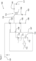
- Figure 1 shows an example of a half-bridge circuit 100.
- the half-bridge circuit 100 comprises a power supply input node 101 couplable to a supply voltage. It will be appreciated that the power supply input node 101 will be coupled to a supply voltage in use and may also be connected to the supply voltage when not in use. However, the power supply input node 101 does not need to be permanently coupled to the supply voltage.
- the half-bridge circuit 100 also comprises an energy storage component 102 configured to store a charge thereon.
- the charge on the energy storage device 102 may be stored thereon as a result of the configuration of the circuit 100 being set such that charge flows to a first plate or other part of the energy storage component via a first node of the energy storage component 102.
- the energy storage component 102 may further have a second node coupled to a second plate or other part of the energy storage component 102 wherein the second node of the energy storage component 102 is coupled to a reference node 103.
- the energy storage component 102 may be a capacitor, such as a resonant capacitor (a capacitor used to resonate with an inductor to assure efficient switching for improved efficiency), a super capacitor or any other component which is configured to store a charge thereon and which can further discharge the charge therefrom.
- a resonant capacitor a capacitor used to resonate with an inductor to assure efficient switching for improved efficiency
- a super capacitor any other component which is configured to store a charge thereon and which can further discharge the charge therefrom.
- Any reference node referred to herein may comprise a node that is couplable to a ground node set to a relative 0 volts. Any reference node may be couplable to a node set to a same relative voltage as one or more of the other reference nodes, or one or more reference nodes may be couplable to nodes set at different reference voltages, as is appropriate to enable operation of the circuit in the described manner. It will further be appreciated that, typically, reference nodes, such as a ground node, are only considered coupled to ground when the circuit is coupled to a power source. As such, references to nodes being couplable to ground are understood by the skilled person as being a clear reference that such a circuit does not need to be coupled to a power source to be a circuit according to the present disclosure but is configured to be so coupled in use.
- the half-bridge circuit 100 further comprises a first switch 104.
- the first switch 104 is connected at a first node of the first switch 104 to the power supply node 101.
- a second node of the first switch 104 is coupled to each of the first node of the energy storage component 102.
- Each of the first switch 104 and the second switch 105 are controllable switches which can be selectively operated by a control signal.
- the first and second switches 104, 105 may be transistors. More specifically, the first and second switches 104, 105 may be MOSFET components such as silicon MOSFETs, silicon carbide MOSFETs or Gallium Nitride MOSFETs. It will be appreciated that other example controllable switches may also be viable alternatives without departing from the present disclosure.
- the control circuit 107 is further connected at an intermediate node 108 of the control circuit 107 to each of the second node of the first switch 104, the first node of the second switch 105 and the first node of the energy storage component 102.
- the intermediate node 108 may be a pin of the control circuit 107, for example. In one or more embodiments, the intermediate node 108 may be a high-voltage pin of the control circuit 107.
- the half-bridge circuit 100 may further be configured to detect when the voltage at the energy storage component is below a predetermined discharge voltage.
- the predetermined discharge voltage may be a voltage which, if that voltage remained on the energy storage component 102 prior to start-up of the half-bridge circuit 100, damage would not be caused to the load, the half-bridge circuit 100 itself or any other components.
- the control circuit 107 may be configured to detect the voltage level at the energy storage component 102 in any of a plurality of suitable ways.
- the control circuit 107 may comprise a comparator 113 configured to compare a voltage at a first input node to a reference voltage at a second input node of the comparator 113 wherein the reference voltage is the predetermined discharge voltage and wherein the voltage at the first input node is indicative of the voltage at the first node of the energy storage component 102.
- the comparator 113 may be any suitable comparator 113 such as a MOSFET, an operational amplifier or another component which can be used to compare an input voltage to a reference voltage and provide an output signal that is dependent on the difference therebetween.
- the voltage at the first input terminal of the comparator 113 may not be exactly the same as the voltage of the energy storage component 102, however, it will be indicative of this voltage.
- one or more voltage drops may occur between the energy storage component 102 and the comparator 113.
- the output node of the comparator 113 may be a low-voltage pin of the control circuit 107 or the output node of the comparator 113 may be coupled to one or more other components within the control circuit 107.
- the half-bridge circuit 100 may further comprise a transformer 115 comprising a first node of a first winding coupled to the second node of the first switch 104; the first node of the second switch 105 and the intermediate node 108.
- the transformer 115 may further comprise a second node coupled to the first node of the energy storage component 102 such that the transformer 115 is arranged between the first switch 104 and the energy storage component 102.
- the transformer 115 may provide for stepping up or stepping down of a voltage from the between the first winding and a second winding where the first winding is located on the first side of the half-bridge circuit 100 (such as the input side) and the second winding is located on a second side of the half-bridge circuit 100 (such as the output side).
- the second winding of the transformer 115 may be couplable to a load on the second side of the circuit.
- a diode 116 may further be located between a first node of the second winding and the load wherein the diode 116 is oriented to inhibit or prevent current from flowing from the load to the second winding of the transformer 115.
- a smoothing capacitor 117 may be placed in parallel with the load.
- the half-bridge circuit 100 may comprise an inductor 118 located between the second node of the first switch 104 and the first node of the first winding of the transformer 115.
- the functionality of the inductor is achieved by designing the transformer such that the leakage inductance is part of the transformer. That is, the inductor may be integrated into the transformer design.
- Figure 2 shows an example switch mode power supply 200 that comprises the half-bridge circuit 201 of figure 1 .
- any components said to be coupled may be coupled or connected either directly or indirectly.
- additional components may be located between the two components that are said to be coupled.
Landscapes
- Engineering & Computer Science (AREA)
- Power Engineering (AREA)
- Charge And Discharge Circuits For Batteries Or The Like (AREA)
Abstract
A half-bridge circuit comprising an energy storage component configured to store a charge thereon; a first switch; a second switch; a control circuit configured to control the switching of the first switch and the second switch, wherein the control circuit comprises: a power dissipating component; a discharge switch configured to selectively couple a first node of the power dissipating component to an intermediate node and wherein a second node of the power dissipating component is coupled such that the energy storage component can selectively discharge charge stored thereon via the power dissipating component of the control circuit and wherein the control circuit is further configured to detect when the voltage at the energy storage component is below a predetermined discharge voltage.
Description
- The present disclosure relates to a half-bridge circuit and a switch mode power supply comprising such a half-bridge circuit.
- According to a first aspect of the present disclosure, there is provided a half-bridge circuit comprising: a power supply node couplable to a supply voltage; an energy storage component configured to store a charge thereon; a first switch connected: at a first node of the first switch to the power supply node; and at a second node of the first switch to a first node of the energy storage component, wherein a second node of the energy storage component is connected to a first reference node; a second switch connected: at a first node of the second switch to the second node of the first switch; at the first node of the second switch to the first node of the energy storage component; and at a second node of the second switch to a second reference node; a control circuit configured to control the switching of the first switch and the second switch, wherein the control circuit is further connected at an intermediate node of the control circuit to: the second node of the first switch; the first node of the second switch; and the first node of the energy storage component, wherein the control circuit comprises: a power dissipating component; a discharge switch configured to selectively couple a first node of the power dissipating component to the intermediate node and wherein a second node of the power dissipating component is coupled to a third reference node such that the energy storage component can selectively discharge charge stored thereon via the power dissipating component of the control circuit and wherein the control circuit is further configured to detect when the voltage at the energy storage component is below a predetermined discharge voltage.
- In one or more embodiments, the control circuit may be configured to cause the energy storage component to be discharged after a reset of the half-bridge circuit.
- In one or more embodiments, the reset of the half-bridge circuit may comprise one or more of: disconnection of a load from the half-bridge circuit; operation of the half-bridge circuit in a protection mode; setting an output voltage level of the half-bridge circuit to a lower voltage level; restart of the half-bridge circuit.
- In one or more embodiments, the power dissipating component may be a current source.
- In one or more embodiments, the control circuit may comprise a comparator configured to compare a voltage at a first input node to a reference voltage at a second input node of the comparator wherein the reference voltage is the predetermined discharge voltage and wherein the voltage at the first input node is indicative of the voltage at the first node of the energy storage component.
- In one or more embodiments, the energy storage component may be a resonant capacitor.
- In one or more embodiments, the half-bridge circuit may further comprise a transformer comprising a first node of a first winding coupled to: the second node of the first switch; the first node of the second switch; and the intermediate node, and the transformer further comprising a second node coupled to the first node of the energy storage component such that the transformer is arranged between the first switch and the energy storage component.
- In one or more embodiments, a second winding of the transformer may be coupled to a load.
- In one or more embodiments, the half-bridge circuit may further comprise an inductor arranged between the first switch and the transformer.
- In one or more embodiments, the half-bridge circuit may further comprise a voltage limiting component arranged between the discharge switch and the intermediate node wherein the voltage limiting component is configured to limit the power provided from the energy storage component to both the discharge switch and the power dissipating component.
- In one or more embodiments, the voltage limiting component may be one of a NMOS or a JFET.
- In one or more embodiments, the intermediate node may be coupled to the control circuit at a high-voltage pin of the control circuit.
- In one or more embodiments, an output node of the comparator may be coupled to a low-voltage pin of the control circuit.
- In one or more embodiments, the control circuit may be configured to prevent start-up of the half-bridge circuit if voltage at the energy storage component is greater than the predetermined discharge voltage.
- In one or more embodiments, the control circuit may be configured to prevent start-up of the half-bridge circuit if the voltage at the energy storage component is greater than the predetermined discharge voltage.
- According to a second aspect of the present disclosure, there is provided a switch mode power supply comprising the half-bridge circuit of the first aspect.
- While the disclosure is amenable to various modifications and alternative forms, specifics thereof have been shown by way of example in the drawings and will be described in detail. It should be understood, however, that other embodiments, beyond the particular embodiments described, are possible as well. All modifications, equivalents, and alternative embodiments falling within the spirit and scope of the appended claims are covered as well.
- The above discussion is not intended to represent every example embodiment or every implementation within the scope of the current or future Claim sets. The figures and Detailed Description that follow also exemplify various example embodiments. Various example embodiments may be more completely understood in consideration of the following Detailed Description in connection with the accompanying Drawings.
- One or more embodiments will now be described by way of example only with reference to the accompanying drawings in which:
-
Figure 1 shows an example embodiment of a half-bridge circuit of the present disclosure; and -
Figure 2 shows a switch mode power supply comprising a half-bridge circuit of the present disclosure. - Switch mode power supplies are widely used to convert the mains voltage into a lower voltage which is appropriate for the application. For example, a switch mode power supply can be used to provide power to any of a mobile phone, a laptop, a tablet computer or another electronic device. Since each device has a different required power level, it is necessary to be able to provide a power supply which can switch to the required power for a given device within a reliable and short time period in a manner that is safe and avoids damaging a charging device.
- The present disclosure presents a circuit having a half-bridge topology that can be used to achieve one or more of the above-listed desired goals. In broad terms, a half-bridge topology uses a set of controlled switches to control how an energy storage device, such as a capacitor, stores and discharges energy. Such a half-bridge circuit can be used in a switch mode power supply which can be used in televisions, gaming consoles, laptops, electric bicycle battery chargers, printers and other devices.
-
Figure 1 shows an example of a half-bridge circuit 100. The half-bridge circuit 100 comprises a powersupply input node 101 couplable to a supply voltage. It will be appreciated that the powersupply input node 101 will be coupled to a supply voltage in use and may also be connected to the supply voltage when not in use. However, the powersupply input node 101 does not need to be permanently coupled to the supply voltage. - The half-
bridge circuit 100 also comprises anenergy storage component 102 configured to store a charge thereon. The charge on theenergy storage device 102 may be stored thereon as a result of the configuration of thecircuit 100 being set such that charge flows to a first plate or other part of the energy storage component via a first node of theenergy storage component 102. Theenergy storage component 102 may further have a second node coupled to a second plate or other part of theenergy storage component 102 wherein the second node of theenergy storage component 102 is coupled to areference node 103. - The
energy storage component 102 may be a capacitor, such as a resonant capacitor (a capacitor used to resonate with an inductor to assure efficient switching for improved efficiency), a super capacitor or any other component which is configured to store a charge thereon and which can further discharge the charge therefrom. - Any reference node referred to herein may comprise a node that is couplable to a ground node set to a relative 0 volts. Any reference node may be couplable to a node set to a same relative voltage as one or more of the other reference nodes, or one or more reference nodes may be couplable to nodes set at different reference voltages, as is appropriate to enable operation of the circuit in the described manner. It will further be appreciated that, typically, reference nodes, such as a ground node, are only considered coupled to ground when the circuit is coupled to a power source. As such, references to nodes being couplable to ground are understood by the skilled person as being a clear reference that such a circuit does not need to be coupled to a power source to be a circuit according to the present disclosure but is configured to be so coupled in use.
- The half-
bridge circuit 100 further comprises afirst switch 104. Thefirst switch 104 is connected at a first node of thefirst switch 104 to thepower supply node 101. A second node of thefirst switch 104 is coupled to each of the first node of theenergy storage component 102. - The half-
bridge circuit 100 further comprises asecond switch 105. Thesecond switch 105 is connected at a first node of thesecond switch 105 to the second node of thefirst switch 104. The first node of thesecond switch 105 is further connected to the first node of theenergy storage component 102. A second node of thesecond switch 105 is coupled to asecond reference node 106. - Each of the
first switch 104 and thesecond switch 105 are controllable switches which can be selectively operated by a control signal. The first andsecond switches second switches - It will be appreciated that where it is described that a particular component is connected to or coupled to another component of the circuit, the two components may be directly connected without intervening components or they may be connected via one or more other components. Where a first node of a particular component is described as coupled to a first node of another component, this is intended to mean that the first node of that particular component is the most directly connected node to the other component. For example, saying that the first node of a first component is connected to a first node of a second component does not mean that the first node of the first component is connected to the first node of the second component via a second node of the first component. As a whole, this phrasing has been used in order to clearly define the order in which certain components are placed in a circuit without limiting the disclosure such that no other additional components could be incorporated between the components in question.
- The half-
bridge circuit 100 further comprises acontrol circuit 107 configured to control the switching of thefirst switch 104 and thesecond switch 105. Thecontrol circuit 107 may be an integrated circuit (IC). Thecontrol circuit 107 may provide for control of thefirst switch 104 and thesecond switch 105 by providing a respective first control signal and second control signal to corresponding control nodes of thefirst switch 104 and thesecond switch 105. - The
control circuit 107 is further connected at anintermediate node 108 of thecontrol circuit 107 to each of the second node of thefirst switch 104, the first node of thesecond switch 105 and the first node of theenergy storage component 102. Theintermediate node 108 may be a pin of thecontrol circuit 107, for example. In one or more embodiments, theintermediate node 108 may be a high-voltage pin of thecontrol circuit 107. - The
control circuit 107 comprises apower dissipating component 110. Thepower dissipating component 110 is a component through which charge from theenergy storage component 102 can be safely discharged. Thepower dissipating component 110 may be a current limiting component which is configured to control the current which passes therethrough. In alternative embodiments, thepower dissipating component 110 may be a voltage dissipating component. For example, theenergy storage component 110 may be a resistor having a resistance configured to provide for safe dissipation of the charge therethrough. In other examples, thepower dissipating component 110 may be a current source. In yet other examples, thepower dissipating component 110 may be another resistive element which allows for controlled discharge of the charge on the energy storage component therethrough. A current source may allow for quicker discharging of the capacitor than a suitable resistor. - The
control circuit 107 may further comprise adischarge switch 111 which is configured to selectively couple a first node of thepower dissipating component 110 to theintermediate node 108 and wherein a second node of thepower dissipating component 110 is coupled to athird reference node 112 such that theenergy storage component 102 can selectively discharge charge stored thereon via thepower dissipating component 110 of thecontrol circuit 107. In one or more embodiments, thedischarge switch 111 may be configured to provide for the discharging of any charge stored on theenergy storage component 102 when thedischarge switch 111 is closed, thereby electrically connecting theenergy storage component 102 to thepower dissipating component 110. Thedischarge switch 111 may be any suitable controllable switch. Thedischarge switch 111 may be controlled by thecontrol circuit 107 such that thecontrol circuit 107 can selectively control the discharge of theenergy storage component 102. - The
control circuit 107 may be configured to cause theenergy storage component 102 to be discharged after a reset of the half-bridge circuit 100. Control of the discharging of theenergy storage component 102 is controlled, at least in part, by way of control of thedischarge switch 111. Reset of the half-bridge circuit 100 may comprise one or more of: disconnection of a load from the half-bridge circuit 100; operation of the half-bridge circuit 100 in a protection mode; and restart of the half-bridge circuit 100 after a shut-down. It will be appreciated that this is not an exhaustive list of the possible conditions under which anenergy storage device 102 may need to be discharged, however, it provides examples that illustrate scenarios in which undischarged charge may otherwise be stored on theenergy storage component 102. By providing for the discharging of the excess charge, potential damage to a load or the half-bridge circuit 100 itself may be avoided. - The
control circuit 107 may be configured to prevent start-up of the half-bridge circuit 100 if the voltage at theenergy storage component 102 is greater than the predetermined discharge voltage. In this way, thecontrol circuit 107 is able to prevent damage from being caused to the load, the half-bridge circuit 100 itself or another component. There may be one or more additional conditions under which thecontrol circuit 107 will prevent start-up of the half-bridge circuit 100. For example, thecontrol circuit 107 may prevent start-up of the half-bridge circuit 100 where the temperature of thecontrol circuit 107 is greater than a predetermined maximum operating temperature. Thecontrol circuit 107 may comprise one or more temperature sensors configured to measure the temperature of thecontrol circuit 107 or thecontrol circuit 107 may be configured to receive a temperature signal indicative of the temperature of thecontrol circuit 100. Thecontrol circuit 107 may further be configured to prevent the start-up of the half-bridge circuit 100 when the input voltage is less than a predetermined minimum input voltage. Acontrol circuit 107 configured to provide for these various protections may provide a particularly safe system and may also be resistant to shorts of one or both of the first andsecond switches - The half-
bridge circuit 100 may further be configured to detect when the voltage at the energy storage component is below a predetermined discharge voltage. The predetermined discharge voltage may be a voltage which, if that voltage remained on theenergy storage component 102 prior to start-up of the half-bridge circuit 100, damage would not be caused to the load, the half-bridge circuit 100 itself or any other components. Thecontrol circuit 107 may be configured to detect the voltage level at theenergy storage component 102 in any of a plurality of suitable ways. In one or more embodiments, thecontrol circuit 107 may comprise acomparator 113 configured to compare a voltage at a first input node to a reference voltage at a second input node of thecomparator 113 wherein the reference voltage is the predetermined discharge voltage and wherein the voltage at the first input node is indicative of the voltage at the first node of theenergy storage component 102. Thecomparator 113 may be anysuitable comparator 113 such as a MOSFET, an operational amplifier or another component which can be used to compare an input voltage to a reference voltage and provide an output signal that is dependent on the difference therebetween. The voltage at the first input terminal of thecomparator 113 may not be exactly the same as the voltage of theenergy storage component 102, however, it will be indicative of this voltage. For example, one or more voltage drops may occur between theenergy storage component 102 and thecomparator 113. In addition, there may be one or more components between theenergy storage component 102 and thecomparator 113 which are configured to intentionally limit the voltage travelling therebetween so that thecomparator 113 and thepower dissipating component 112 can operate at a reduced voltage. The output node of thecomparator 113 may be a low-voltage pin of thecontrol circuit 107 or the output node of thecomparator 113 may be coupled to one or more other components within thecontrol circuit 107. - In one or more embodiments, the
control circuit 107 may comprise avoltage limiting component 114 arranged between thedischarge switch 111 and theintermediate node 108. Thevoltage limiting component 114 may be configured to limit the voltage provided from theenergy storage component 102 to both thedischarge switch 111 and thepower dissipating component 110 to below a maximum threshold voltage. In one or more embodiments, thevoltage limiting component 114 may be configured to provide for a maximum threshold voltage that can pass therethrough such that thedischarge switch 111 andpower dissipating component 110 do not experience voltages above the maximum threshold voltage. This allows the components below the voltage limiting component in the circuit, as shown, to be selected to have a maximum operating voltage based on the maximum threshold voltage. This allows the maximum operating voltage of these components to be selected such that they do not exceed, or do not significantly exceed the maximum threshold voltage, thereby allowing for the selection of components that are one or both of smaller and cheaper than would be necessary if they needed to be configured to handle higher voltages. Thevoltage limiting component 114 may be one of an NMOS or a JFET, for example. The provision of thevoltage limiting component 114 means that the total power dissipation is split between thevoltage limiting component 114 and thepower dissipating component 110. It will be appreciated that, for correct operation, the maximum threshold voltage will be greater than the reference voltage at the second input node of the comparator. - The half-
bridge circuit 100 may further comprise atransformer 115 comprising a first node of a first winding coupled to the second node of thefirst switch 104; the first node of thesecond switch 105 and theintermediate node 108. Thetransformer 115 may further comprise a second node coupled to the first node of theenergy storage component 102 such that thetransformer 115 is arranged between thefirst switch 104 and theenergy storage component 102. Thetransformer 115 may provide for stepping up or stepping down of a voltage from the between the first winding and a second winding where the first winding is located on the first side of the half-bridge circuit 100 (such as the input side) and the second winding is located on a second side of the half-bridge circuit 100 (such as the output side). The second winding of thetransformer 115 may be couplable to a load on the second side of the circuit. Adiode 116 may further be located between a first node of the second winding and the load wherein thediode 116 is oriented to inhibit or prevent current from flowing from the load to the second winding of thetransformer 115. A smoothingcapacitor 117 may be placed in parallel with the load. - The half-
bridge circuit 100 may comprise aninductor 118 located between the second node of thefirst switch 104 and the first node of the first winding of thetransformer 115. In some examples, the functionality of the inductor is achieved by designing the transformer such that the leakage inductance is part of the transformer. That is, the inductor may be integrated into the transformer design. -
Figure 2 shows an example switchmode power supply 200 that comprises the half-bridge circuit 201 offigure 1 . - It will be appreciated that any components said to be coupled may be coupled or connected either directly or indirectly. In the case of indirect coupling, additional components may be located between the two components that are said to be coupled.
- In this specification, example embodiments have been presented in terms of a selected set of details. However, a person of ordinary skill in the art would understand that many other example embodiments may be practiced which include a different selected set of these details. It is intended that the following claims cover all possible example embodiments.
Claims (15)
- A half-bridge circuit comprising:a power supply node couplable to a supply voltage;an energy storage component configured to store a charge thereon;a first switch connected:at a first node of the first switch to the power supply node; andat a second node of the first switch to a first node of the energy storage component, wherein a second node of the energy storagecomponent is connected to a first reference node;a second switch connected:at a first node of the second switch to the second node of the first switch;at the first node of the second switch to the first node of the energy storage component; andat a second node of the second switch to a second reference node;a control circuit configured to control the switching of the first switch and the second switch, wherein the control circuit is further connected at an intermediate node of the control circuit to:wherein the control circuit comprises:the second node of the first switch;the first node of the second switch; andthe first node of the energy storage component,a power dissipating component;a discharge switch configured to selectively couple a first node of the power dissipating component to the intermediate node and wherein a second node of the power dissipating component is coupled to a third reference node such that the energy storage component can selectively discharge charge stored thereon via the power dissipating component of the control circuit and wherein the control circuit is further configured to detect when the voltage at the energy storage component is below a predetermined discharge voltage.
- The half-bridge circuit of claim 1 wherein the control circuit is configured to cause the energy storage component to be discharged after a reset of the half-bridge circuit.
- The half-bridge circuit of claim 2 wherein the reset of the half-bridge circuit comprises one or more of:disconnection of a load from the half-bridge circuit;operation of the half-bridge circuit in a protection mode;setting an output voltage level of the half-bridge circuit to a lower voltage level;restart of the half-bridge circuit.
- The half-bridge circuit of any preceding wherein the power dissipating component is a current source.
- The half-bridge circuit of any preceding claim wherein the control circuit comprises a comparator configured to compare a voltage at a first input node to a reference voltage at a second input node of the comparator wherein the reference voltage is the predetermined discharge voltage and wherein the voltage at the first input node is indicative of the voltage at the first node of the energy storage component.
- The half-bridge circuit of any preceding claim wherein the energy storage component is a resonant capacitor.
- The half-bridge circuit of any preceding claim further comprising a transformer comprising a first node of a first winding coupled to:the second node of the first switch;the first node of the second switch; andthe intermediate node,and the transformer further comprising a second node coupled to the first node of the energy storage component such that the transformer is arranged between the first switch and the energy storage component.
- The half-bridge circuit of claim 7 wherein a second winding of the transformer is coupled to a load.
- The half-bridge circuit of either of claims 7 - 8 further comprising an inductor arranged between the first switch and the transformer.
- The half-bridge circuit of any preceding claim further comprising a voltage limiting component arranged between the discharge switch and the intermediate node wherein the voltage limiting component is configured to limit the power provided from the energy storage component to both the discharge switch and the power dissipating component.
- The half-bridge circuit of claim 10 wherein the voltage limiting component is one of a NMOS or a JFET.
- The half-bridge circuit of any preceding claim wherein the intermediate node is coupled to the control circuit at a high-voltage pin of the control circuit.
- The half-bridge circuit of any preceding claim wherein the control circuit is configured to prevent start-up of the half-bridge circuit if voltage at the energy storage component is greater than the predetermined discharge voltage.
- The half-bridge circuit of any preceding claim wherein the control circuit is configured to prevent start-up of the half-bridge circuit if the voltage at the energy storage component is greater than the predetermined discharge voltage.
- A switch mode power supply comprising the half-bridge circuit of any of claims 1 - 14.
Priority Applications (1)
| Application Number | Priority Date | Filing Date | Title |
|---|---|---|---|
| EP23194369.7A EP4518129A1 (en) | 2023-08-30 | 2023-08-30 | A half-bridge circuit |
Applications Claiming Priority (1)
| Application Number | Priority Date | Filing Date | Title |
|---|---|---|---|
| EP23194369.7A EP4518129A1 (en) | 2023-08-30 | 2023-08-30 | A half-bridge circuit |
Publications (1)
| Publication Number | Publication Date |
|---|---|
| EP4518129A1 true EP4518129A1 (en) | 2025-03-05 |
Family
ID=87889391
Family Applications (1)
| Application Number | Title | Priority Date | Filing Date |
|---|---|---|---|
| EP23194369.7A Withdrawn EP4518129A1 (en) | 2023-08-30 | 2023-08-30 | A half-bridge circuit |
Country Status (1)
| Country | Link |
|---|---|
| EP (1) | EP4518129A1 (en) |
Citations (4)
| Publication number | Priority date | Publication date | Assignee | Title |
|---|---|---|---|---|
| US7141958B2 (en) * | 2003-05-12 | 2006-11-28 | International Business Machines Corporation | Power supply apparatus and power supply control device |
| US20150263602A1 (en) * | 2014-03-17 | 2015-09-17 | Semiconductor Components Industries, Llc | Method and semiconductor device for a dedicated startup sequence in a resonant converter |
| WO2021224021A1 (en) * | 2020-05-04 | 2021-11-11 | Tridonic Gmbh & Co Kg | Power converter with overshoot protection |
| CN116599352A (en) * | 2023-05-05 | 2023-08-15 | 深圳市必易微电子股份有限公司 | Asymmetric half-bridge flyback circuit and control method thereof |
-
2023
- 2023-08-30 EP EP23194369.7A patent/EP4518129A1/en not_active Withdrawn
Patent Citations (4)
| Publication number | Priority date | Publication date | Assignee | Title |
|---|---|---|---|---|
| US7141958B2 (en) * | 2003-05-12 | 2006-11-28 | International Business Machines Corporation | Power supply apparatus and power supply control device |
| US20150263602A1 (en) * | 2014-03-17 | 2015-09-17 | Semiconductor Components Industries, Llc | Method and semiconductor device for a dedicated startup sequence in a resonant converter |
| WO2021224021A1 (en) * | 2020-05-04 | 2021-11-11 | Tridonic Gmbh & Co Kg | Power converter with overshoot protection |
| CN116599352A (en) * | 2023-05-05 | 2023-08-15 | 深圳市必易微电子股份有限公司 | Asymmetric half-bridge flyback circuit and control method thereof |
Similar Documents
| Publication | Publication Date | Title |
|---|---|---|
| EP3163711B1 (en) | Uninterruptible power supply unit | |
| US9373977B1 (en) | Battery backup system for uninterrupted power supply | |
| US8848321B2 (en) | SMPS having a safety arrangement, a method of operating a SMPS, and a controller therefor | |
| JP5567684B2 (en) | Battery balancing circuit and method for balancing energy stored in a plurality of cells of a battery having a first terminal and a second terminal | |
| US9906145B2 (en) | Power converter with load switch fault protection | |
| US20170366091A1 (en) | Isolated power converter with output voltage protection | |
| WO2012049910A1 (en) | Output circuit for electric power supply system | |
| US20110057626A1 (en) | Power supply and charging circuit for high energy capacitors | |
| US20120087154A1 (en) | Voltage supply device for a load | |
| CN109874366B (en) | Electric machine and apparatus | |
| US6804126B2 (en) | Power supply start up circuit | |
| CN107342603B (en) | Battery Control Circuits for Power Generation Systems Using Renewable Energy | |
| CN108306495A (en) | Dual-stage Vcc chargings for switch mode power | |
| CN111049203A (en) | Charge and discharge management circuit and chargeable electronic equipment | |
| CN101989830A (en) | Static exciter of a field winding and method for operating the same | |
| CN119051459A (en) | Power supply circuit, energy storage converter and energy storage system | |
| US11894771B2 (en) | Current control circuit | |
| KR20210017051A (en) | Overvoltage protection circuit and operation method thereof | |
| KR101639885B1 (en) | Constant voltage source battery assist device and battery pack comrising the same | |
| CN113949031A (en) | Power supply device of motor protector and power supply method thereof | |
| JPH11289657A (en) | Inrush current suppressor | |
| US6577485B2 (en) | Ultra-wide input range power supply for circuit protection devices | |
| US12418169B2 (en) | Direct current/direct current converter and control method thereof | |
| KR102580366B1 (en) | Wireless Power Receiver Having Input Power Blocking Circuit | |
| KR101058351B1 (en) | Battery charge / discharge control circuit with regulator and inverter |
Legal Events
| Date | Code | Title | Description |
|---|---|---|---|
| PUAI | Public reference made under article 153(3) epc to a published international application that has entered the european phase |
Free format text: ORIGINAL CODE: 0009012 |
|
| STAA | Information on the status of an ep patent application or granted ep patent |
Free format text: STATUS: THE APPLICATION HAS BEEN PUBLISHED |
|
| AK | Designated contracting states |
Kind code of ref document: A1 Designated state(s): AL AT BE BG CH CY CZ DE DK EE ES FI FR GB GR HR HU IE IS IT LI LT LU LV MC ME MK MT NL NO PL PT RO RS SE SI SK SM TR |
|
| STAA | Information on the status of an ep patent application or granted ep patent |
Free format text: STATUS: THE APPLICATION IS DEEMED TO BE WITHDRAWN |
|
| 18D | Application deemed to be withdrawn |
Effective date: 20250906 |