EP4517822A1 - Halbleiterstruktur und herstellungsverfahren dafür - Google Patents
Halbleiterstruktur und herstellungsverfahren dafür Download PDFInfo
- Publication number
- EP4517822A1 EP4517822A1 EP24769813.7A EP24769813A EP4517822A1 EP 4517822 A1 EP4517822 A1 EP 4517822A1 EP 24769813 A EP24769813 A EP 24769813A EP 4517822 A1 EP4517822 A1 EP 4517822A1
- Authority
- EP
- European Patent Office
- Prior art keywords
- semiconductor
- word line
- channel
- isolation
- air gap
- Prior art date
- Legal status (The legal status is an assumption and is not a legal conclusion. Google has not performed a legal analysis and makes no representation as to the accuracy of the status listed.)
- Pending
Links
Images


Classifications
-
- H—ELECTRICITY
- H10—SEMICONDUCTOR DEVICES; ELECTRIC SOLID-STATE DEVICES NOT OTHERWISE PROVIDED FOR
- H10D—INORGANIC ELECTRIC SEMICONDUCTOR DEVICES
- H10D30/00—Field-effect transistors [FET]
- H10D30/60—Insulated-gate field-effect transistors [IGFET]
- H10D30/67—Thin-film transistors [TFT]
- H10D30/6728—Vertical TFTs
-
- H—ELECTRICITY
- H10—SEMICONDUCTOR DEVICES; ELECTRIC SOLID-STATE DEVICES NOT OTHERWISE PROVIDED FOR
- H10B—ELECTRONIC MEMORY DEVICES
- H10B12/00—Dynamic random access memory [DRAM] devices
- H10B12/01—Manufacture or treatment
- H10B12/02—Manufacture or treatment for one transistor one-capacitor [1T-1C] memory cells
- H10B12/05—Making the transistor
-
- H—ELECTRICITY
- H10—SEMICONDUCTOR DEVICES; ELECTRIC SOLID-STATE DEVICES NOT OTHERWISE PROVIDED FOR
- H10B—ELECTRONIC MEMORY DEVICES
- H10B12/00—Dynamic random access memory [DRAM] devices
- H10B12/30—DRAM devices comprising one-transistor - one-capacitor [1T-1C] memory cells
- H10B12/48—Data lines or contacts therefor
- H10B12/482—Bit lines
-
- H—ELECTRICITY
- H10—SEMICONDUCTOR DEVICES; ELECTRIC SOLID-STATE DEVICES NOT OTHERWISE PROVIDED FOR
- H10B—ELECTRONIC MEMORY DEVICES
- H10B12/00—Dynamic random access memory [DRAM] devices
- H10B12/30—DRAM devices comprising one-transistor - one-capacitor [1T-1C] memory cells
- H10B12/48—Data lines or contacts therefor
- H10B12/488—Word lines
-
- H—ELECTRICITY
- H10—SEMICONDUCTOR DEVICES; ELECTRIC SOLID-STATE DEVICES NOT OTHERWISE PROVIDED FOR
- H10D—INORGANIC ELECTRIC SEMICONDUCTOR DEVICES
- H10D30/00—Field-effect transistors [FET]
- H10D30/01—Manufacture or treatment
- H10D30/021—Manufacture or treatment of FETs having insulated gates [IGFET]
- H10D30/025—Manufacture or treatment of FETs having insulated gates [IGFET] of vertical IGFETs
-
- H—ELECTRICITY
- H10—SEMICONDUCTOR DEVICES; ELECTRIC SOLID-STATE DEVICES NOT OTHERWISE PROVIDED FOR
- H10D—INORGANIC ELECTRIC SEMICONDUCTOR DEVICES
- H10D30/00—Field-effect transistors [FET]
- H10D30/60—Insulated-gate field-effect transistors [IGFET]
- H10D30/63—Vertical IGFETs
-
- H—ELECTRICITY
- H10—SEMICONDUCTOR DEVICES; ELECTRIC SOLID-STATE DEVICES NOT OTHERWISE PROVIDED FOR
- H10B—ELECTRONIC MEMORY DEVICES
- H10B12/00—Dynamic random access memory [DRAM] devices
- H10B12/30—DRAM devices comprising one-transistor - one-capacitor [1T-1C] memory cells
- H10B12/31—DRAM devices comprising one-transistor - one-capacitor [1T-1C] memory cells having a storage electrode stacked over the transistor
- H10B12/315—DRAM devices comprising one-transistor - one-capacitor [1T-1C] memory cells having a storage electrode stacked over the transistor with the capacitor higher than a bit line
Definitions
- This application relates to the field of integrated circuit technologies, and in particular, to a semiconductor structure and a manufacturing method therefor.
- DRAM dynamic random access memory
- this application provides a semiconductor structure and a manufacturing method therefor, to reduce the volume of a device and reduce the difficulty of a manufacturing process.
- the semiconductor structure includes a semiconductor layer having first isolation trenches extending in the first direction and second isolation trenches extending in the second direction.
- the depth of the first isolation trench is greater than the depth of the second isolation trench, the second direction intersects the first direction, the first isolation trenches isolate multiple semiconductor strips spaced apart in the second direction in the semiconductor layer, and the second isolation trenches isolate multiple semiconductor pillars spaced apart in the first direction in the semiconductor strips.
- the semiconductor pillar includes a channel region and a first doped region and a second doped region respectively disposed at the upper end and the lower end of the channel region in the extension direction of the semiconductor pillar.
- the semiconductor structure further includes:
- a second air gap is formed below the first word line.
- the bit line is formed on a bottom surface of the bit line contact structure.
- a gate dielectric layer covering a sidewall of the semiconductor pillar in the first direction is formed.
- the word line is formed on a sidewall of the gate dielectric layer away from the semiconductor pillar.
- two staggered word lines are formed on two opposite sidewalls of the semiconductor pillar while the two word lines are enabled to jointly constitute a control word line corresponding to the semiconductor pillar, so that space between adjacent semiconductor pillars can be reduced, thereby reducing the volume of a device.
- ends of the semiconductor pillars connected to the bit lines are shorted together, so that the volume of the device can be further reduced, and a contact resistance between the bit line and the semiconductor pillar can also be reduced.
- the second isolation trench in the semiconductor structure and the manufacturing method therefor provided in this application is shallower than a trench in a conventional semiconductor structure. Therefore, the difficulty of a manufacturing process can be further reduced.
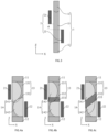
- the multiple word lines 2 and the multiple semiconductor pillars 1 may be alternately arranged in the first direction (e.g., the X direction), and two word lines 2 located on two sides of the same semiconductor pillar 1 may be staggered in an extension direction of the semiconductor pillar 1, and jointly constitute a control word line corresponding to the semiconductor pillar 1.
- the material of the semiconductor pillar 1 is not specifically limited in this application.
- the material of the semiconductor pillar 1 may include silicon (Si), silicon germanium (SiGe), silicon germanium carbon (SiGeC), silicon carbide (SiC), gallium arsenide (GaAs), indium arsenide (InAs), indium phosphide (InP), or another III/V semiconductor material or II/VI semiconductor material.
- adjacent semiconductor pillars 1 may share the same first word line 21 or second word line 22 while the first word line 21 or the second word line 22 is enabled to be a part of a control word line corresponding to the semiconductor pillars 1, so that space between adjacent semiconductor pillars 1 can be reduced, thereby reducing the volume of the device.
- the disposition manner in which adjacent semiconductor pillars 1 share the same first word line 21 or second word line 22 can further make the internal layout of the semiconductor structure more proper, so that the storage density of the semiconductor structure is effectively increased.
- adjacent semiconductor pillars 1 may share the same first word line 21 or second word line 22.
- two adjacent semiconductor pillars 1 in the first direction (e.g., the X direction) may share a first word line 21 located between the semiconductor pillar 1A and the semiconductor pillar 1B.
- the semiconductor pillar 1 may specifically include a first doped region 11, a second doped region 12, and a channel region 13.
- the first doped region 11 and the second doped region 12 may be respectively disposed at the upper end and the lower end of the channel region 13 in an extension direction (e.g., a Z direction) of the channel region 13.
- the two word lines 2 located on the two sides of the same semiconductor pillar 1 may be respectively disposed on sidewalls of the channel region 13.
- a location relationship between the two word lines 2 located on the two sides of the same semiconductor pillar 1 is not specifically limited in this application. Further referring to FIG. 3 , in some embodiments, projections of the two word lines 2 located on the two sides of the same semiconductor pillar 1 in the channel region 13 toward the substrate do not overlap.
- the channel region 13 may specifically include a first channel 131 and a second channel 132.
- the first channel 131 is close to the first doped region 11 or at least partially connected to the first doped region 11.
- the first word line 21 is located on a first-side sidewall of the first channel 131, and a part of the first channel 131 close to the first-side sidewall is capable of forming a first inversion layer 141 in response to an electrical signal of the first word line 21.
- the second channel 132 is close to the second doped region 12 or at least partially connected to the second doped region 12.
- the second word line 22 is located on a second-side sidewall of the first channel 131, and a part of the second channel 132 close to the second-side sidewall is capable of forming a second inversion layer 142 in response to an electrical signal of the second word line 22.
- the first channel 131 may not overlap the second channel 132.
- both the first inversion layer 141 and the second inversion layer 142 are inversion layers (Inversion layer).
- the inversion layer refers to a region in which a free carrier is opposite to a semiconductor carrier formed by doping under the action of an electric field generated by an electrical signal.
- the inversion layer may also be referred to as a conductive channel.
- a doping type of a semiconductor pillar 1 in which the first channel 131 is located nor a doping type of a semiconductor pillar 1 in which the second channel 132 is located is specifically limited in this application.
- the doping type of the semiconductor pillar 1 in which the first channel 131 is located may be the same as the doping type of the semiconductor pillar 1 in which the second channel 132 is located.
- the doping type of the first doped region 11 and the doping type of the second doped region 12 each may be N-type doping, and correspondingly, the doping type of the semiconductor pillar 1 in which the first channel 131 is located and the doping type of the semiconductor pillar 1 in which the second channel 132 is located each may be P-type doping.
- a doping concentration of the first channel 131 and a doping concentration of the second channel 132 are not specifically limited in this application, either.
- the doping concentration of the first channel 131 may be the same as or close to the doping concentration of the second channel 132.
- the channel region 13 may further include an isolation channel 133.
- the isolation channel 133 is located between the first channel 131 and the second channel 132.
- the isolation channel 133 may be configured to isolate the first inversion layer 141 and the second inversion layer 142.
- a disposition manner of the isolation channel 133 is not specifically limited in this application.
- the isolation channel 133 may extend in a direction parallel to the first direction (e.g., the X direction).
- the isolation channel 133 overlaps the projection of the first word line 21 in the channel region 13 toward the substrate, or the isolation channel 133 overlaps the projection of the second word line 22 in the channel region 13 toward the substrate, or the isolation channel 133 overlaps both the projection of the first word line 21 in the channel region 13 toward the substrate and the projection of the second word line 22 in the channel region 13 toward the substrate.
- the isolation channel 133 may alternatively extend in a direction intersecting the first direction (e.g., the X direction).
- the isolation channel 133 may include a first-side end surface and a second-side end surface disposed opposite to each other in the extension direction of the isolation channel 133.
- the first-side end surface is located on a side of the first channel 131 close to the second channel 132, and the first-side end surface is located outside the projection of the first word line 21 in the channel region 13 toward the substrate, and the second-side end surface is located on a side of the second channel 132 close to the first channel 131, and the second-side end surface is located outside the projection of the second word line 22 in the channel region 13 toward the substrate.
- a doping type of a semiconductor pillar 1 in which the isolation channel 133 is located is not specifically limited in this application. In some embodiments, all of the doping type of the semiconductor pillar 1 in which the first channel 131 is located, the doping type of the semiconductor pillar 1 in which the second channel 132 is located, and the doping type of the semiconductor pillar 1 in which the isolation channel 133 is located are the same. For example, the doping type of the semiconductor pillar 1 in which the first channel 131 is located, the doping type of the semiconductor pillar 1 in which the second channel 132 is located, and the doping type of the semiconductor pillar 1 in which the isolation channel 133 is located each are P-type doping.
- the semiconductor structure may include a semiconductor layer 100, multiple bit lines 3 extending in the first direction (e.g., the X direction) and being spaced apart in the second direction (e.g., the Y direction), and multiple word lines 2 extending in the second direction (e.g., the Y direction) and being spaced apart in the first direction (e.g., the X direction).
- the two word lines 2 on the two opposite sidewalls of the semiconductor pillar 1 are staggered while the two word lines 2 are enabled to jointly constitute the control word line 2 corresponding to the semiconductor pillar 1, so that space between adjacent semiconductor pillars 1 can be reduced, thereby reducing the volume of the device.
- the second isolation trench T2 in the semiconductor structure is shallower than a trench in a conventional semiconductor structure. Therefore, the difficulty of a manufacturing process can be further reduced.
- a top surface of the second word line 22 may be flush with a bottom surface of the first word line 21; or a top surface of the second word line 22 may be lower than a bottom surface of the first word line 21.
- the width of the second word line 22 is not specifically limited in this application. In some embodiments, the width of the second word line 22 may gradually increase in a direction away from the bottom portion of the second isolation trench T2.
- the shape of the second word line 22 is not specifically limited in this application. In some embodiments, the shape of an end portion of the second word line 22 close to the bottom portion of the second isolation trench T2 may be similar to that of the bottom portion of the second isolation trench T2.
- the air gap structure 7 is located in the second isolation trench T2, and the air gap structure 7 may include a first air gap 71 and/or a second air gap 72.
- the first air gap 71 is located above the second word line 22, and the second air gap 72 is located below the first word line 21.
- the air gap structure 7 in the second isolation trench T2 can reduce a floating body effect between adjacent semiconductor pillars 1, to further reduce static leakage of the device in a use process.
- the location of the first air gap 71 is not specifically limited in this application, provided that the first air gap 71 is located above the second word line 22.
- an orthographic projection of the first air gap 71 on the semiconductor pillar 1 may overlap or approximately overlap an orthographic projection of the first word line 21 on the semiconductor pillar 1.
- the location of the second air gap 72 is not specifically limited in this application, either, provided that the second air gap 72 is located below the first word line 21.
- an orthographic projection of the second air gap 72 on the semiconductor pillar 1 may overlap or approximately overlap an orthographic projection of the second word line 22 on the semiconductor pillar 1.
- the semiconductor structure may further include a first isolation structure 51 and a second isolation structure 52.
- the first isolation structure 51 is located in the first isolation trench T1, and may be configured to fill a spacing between adjacent semiconductor strips 10.
- the second isolation structure 52 is located in the second isolation trench T2, and may be configured to fill a spacing between adjacent semiconductor pillars 1 in the first direction (e.g., the X direction) and cover the word line 2.
- the second isolation structure 52 may be further configured to seal the air gap structure 7.
- the materials of the first isolation structure 51 and the second isolation structure 52 are not specifically limited in this application.
- the material of the first isolation structure 51 may be the same as the material of the second isolation structure 52.
- the first isolation structure 51 and the second isolation structure 52 may actually be presented as an integral structure.
- the material of the first isolation structure 51 and the material of the second isolation structure 52 each may include but are not limited to silicon nitride (SiN), silicon oxynitride (SiON), silicon dioxide (SiO 2 ), or the like, or a combination thereof.
- a location relationship between the first air gap 71 and the first word line 21 is not specifically limited in this application.
- a bottom surface of the first air gap 71 may be flush with the bottom surface of the first word line 21; or a bottom surface of the first air gap 71 may be lower than the bottom surface of the first word line 21.
- a top surface of the first air gap 71 may be flush with a top surface of the first word line 21; or a top surface of the first air gap 71 may be higher than a top surface of the first word line 21.
- a location relationship between the second air gap 72 and the second word line 22 is not specifically limited in this application.
- a top surface of the second air gap 72 may be flush with the top surface of the second word line 22; or a top surface of the second air gap 72 may be higher than the top surface of the second word line 22.
- a bottom surface of the second air gap 72 may be flush with the bottom surface of the second word line 22.
- the semiconductor structure may further include a gate dielectric layer 8.
- the gate dielectric layer 8 may cover a sidewall of the semiconductor pillar 1 in the first direction (e.g., the X direction), and is located between the semiconductor pillar 1 and the word line 2.
- the material of the gate dielectric layer 8 is not specifically limited in this application.
- the material of the gate dielectric layer 8 may include but is not limited to one or more of a high-K dielectric material, silicon oxide, silicon nitride, or silicon oxynitride.
- the high-K dielectric material is a material whose relative dielectric constant is greater than a relative dielectric constant of silicon oxide, e.g., hafnium oxide (HfO 2 ) or aluminum oxide (Al 2 O 3 ).
- the structure of the gate dielectric layer 8 is not specifically limited in this application, either.
- the gate dielectric layer 8 may be of a single-layer structure, or may be of a stacked structure.
- the quantity of layers of the gate dielectric layer 8 may be adaptively set based on different actual manufacturing processes and different requirements on the thickness of the gate dielectric layer 8.
- the first word line 21 is formed on a first-side sidewall of the first channel 131.
- a part of the first channel 131 close to the first-side sidewall is capable of forming a first inversion layer 141 in response to an electrical signal of the first word line 21.
- the step of S220 in which the second word line 22 is formed on a partial sidewall of the channel region 13 close to the second doped region 12 may specifically include the step as follows.
- a semiconductor layer is provided, and first isolation trenches extending in a first direction and second isolation trenches extending in a second direction are formed in the semiconductor layer.
- the depth of the first isolation trench is greater than the depth of the second isolation trench, the second direction intersects the first direction, the first isolation trenches isolate multiple semiconductor strips spaced apart in the second direction in the semiconductor layer, and the second isolation trenches isolate multiple semiconductor pillars spaced apart in the first direction in the semiconductor strips.
- bit lines extending in the first direction are respectively formed on bottom surfaces of the multiple semiconductor strips.
- the two staggered word lines may be formed on the two opposite sidewalls of the semiconductor pillar while the two word lines are enabled to jointly constitute the control word line corresponding to the semiconductor pillar, so that space between adjacent semiconductor pillars can be reduced, thereby reducing the volume of a device.
- ends of the semiconductor pillars connected to the bit lines are shorted together, so that the volume of the device can be further reduced, and a contact resistance between the bit line and the semiconductor pillar can also be reduced.
- the second isolation trench formed in the manufacturing method is shallower than a trench in a conventional semiconductor structure. Therefore, the difficulty of a manufacturing process can be further reduced.
- first word lines are respectively formed on upper middle portions of the other second isolation trenches.
- the manufacturing method for a semiconductor structure may further include the step as follows.
- a first isolation structure is formed in the first isolation trench.
- the first isolation structure fills a spacing between adjacent semiconductor strips.
- the manufacturing method for a semiconductor structure may further include the step as follows.
- a second isolation structure is formed in the second isolation trench.
- the second isolation structure fills a spacing between adjacent semiconductor pillars in the first direction and covers the word line.
- a second isolation structure is formed in the second isolation trench may specifically include the steps as follows.
- a first air gap is formed above the second word line.
- a second air gap is formed below the first word line.
- the first air gap and the second air gap jointly constitute an air gap structure, and the second isolation structure further seals the air gap structure.
- the manufacturing method for a semiconductor structure may further include the step as follows.
- Bit line contact structures extending in the first direction are respectively formed on the bottom surfaces of the multiple semiconductor strips.
- the bit line may be formed on a bottom surface of the bit line contact structure.
- the manufacturing method for a semiconductor structure may further include the step as follows.
- a gate dielectric layer covering a sidewall of the semiconductor pillar in the first direction is formed.
- the word line may be formed on a sidewall of the gate dielectric layer away from the semiconductor pillar.
- steps in the flowcharts of FIG. 8 to FIG. 12 are sequentially shown according to indications of the arrows, these steps are not necessarily sequentially performed according to the indications of the arrows. Unless expressly stated in the specification, these steps are not performed in a strict order, and these steps may be performed in another order. In addition, at least some steps in FIG. 8 to FIG. 12 may include multiple steps or multiple phases. These steps or phases are not necessarily performed and completed at the same moment, but may be performed at different moments. These steps or phases are not necessarily sequentially performed, but may be performed in turn or alternately with another step or at least some of the steps or phases in the another step.
- the some embodiments of this application are understood below with reference to FIG. 13 to FIG. 16 . It should be noted that in this embodiment of this application, the second direction intersects the first direction.
- a semiconductor layer 100 is provided.
- first isolation trenches T1 extending in the first direction e.g., the X direction
- the first isolation trenches T1 may isolate multiple semiconductor strips 10 spaced apart in the second direction (e.g., the Y direction) in the semiconductor layer 100.
- second isolation trenches T2 extending in the second direction e.g., the Y direction
- the second isolation trenches T2 may isolate multiple semiconductor pillars 1 spaced apart in the first direction (e.g., the X direction) in the semiconductor strips 10.
- the depth of the first isolation trench T1 is greater than the depth of the second isolation trench T2.
- Manners of forming the first isolation trench T1 and the second isolation trench T2 are not specifically limited in this application.
- the first isolation trench T1 and the second isolation trench T2 may be formed in the semiconductor layer 100 through, but not limited to, the self-aligned double patterning (SADP) process or the self-aligned quadruple patterning (SAQP) process.
- SADP self-aligned double patterning
- SAQP self-aligned quadruple patterning
- the manufacturing method for a semiconductor structure may further include the step as follows.
- a first isolation structure 51 is formed in the first isolation trench T1.
- the first isolation structure 51 may be configured to fill a spacing between adjacent semiconductor strips 10.
- a manner of forming the first isolation structure 51 is not specifically limited in this application.
- the first isolation structure 5 may be formed in the first isolation trench T1 through, but not limited to, a physical vapor deposition (PVD) process, a chemical vapor deposition (CVD) process, or an atomic layer deposition (ALD) process.
- PVD physical vapor deposition
- CVD chemical vapor deposition
- ALD atomic layer deposition
- bit lines extending in the first direction are respectively formed on bottom surfaces of the multiple semiconductor strips 10.
- bit line may be formed on the bottom surface of the semiconductor strip 10 through, but not limited to, a heterogeneous integration technology on chip (HITOC) process.
- HTOC heterogeneous integration technology on chip
- the manufacturing method for a semiconductor structure may further include the step as follows.
- a gate dielectric layer 8 covering a sidewall of the semiconductor pillar 100 in the first direction (e.g., the X direction) is formed.
- a manner of forming the gate dielectric layer 8 is not specifically limited in this application.
- the gate dielectric layer 8 may be formed on a sidewall of the semiconductor pillar 1 through, but not limited to, the atomic layer deposition process, the chemical vapor deposition process, or a rapid thermal oxidation (RTO) process.
- RTO rapid thermal oxidation
- word lines 2 extending in the second direction are respectively formed in the multiple second isolation trenches T2.
- the multiple word lines 2 and the multiple semiconductor pillars 1 are alternately arranged in the first direction (e.g., the X direction), and two word lines 2 on two opposite sidewalls of the same semiconductor pillar 1 are staggered in an extension direction of the semiconductor pillar 1, and jointly constitute a control word line 2 corresponding to the semiconductor pillar 1.
- the manufacturing method for a semiconductor structure may further include the step as follows.
- a second isolation structure 52 is formed in the second isolation trench T2.
- the second isolation structure 52 may be configured to fill a spacing between adjacent semiconductor pillars 1 in the first direction (e.g., the X direction), and may be further configured to cover the word line 2.
- a manner of forming the second isolation structure 52 is not specifically limited in this application.
- the second isolation structure 52 may be formed in the second isolation trench T2 through, but not limited to, the physical vapor deposition process, the chemical vapor deposition process, or the atomic layer deposition process.
- a word line 2 close to a bottom portion of the second isolation trench T2 is a second word line 22
- a word line 2 away from the bottom portion of the second isolation trench T2 is a first word line 21.
- the step of S300 in which word lines 2 extending in the second direction (e.g., the Y direction) are respectively formed in the multiple second isolation trenches T2 may be specifically represented as the steps of S310 and S320 as follows.
- second word lines 22 are respectively formed on bottom portions of some of the second isolation trenches T2.
- first word lines 21 are respectively formed on upper middle portions of the other second isolation trenches T2.
- a top surface of the second word line 22 may be flush with a bottom surface of the first word line 21; or a top surface of the second word line 22 may be lower than a bottom surface of the first word line 21.
- a second isolation structure 52 is formed in the second isolation trench T2 may further include the steps of S410 and S420 as follows.
- a first air gap 71 is formed above the second word line 22.
Landscapes
- Engineering & Computer Science (AREA)
- Manufacturing & Machinery (AREA)
- Semiconductor Memories (AREA)
Applications Claiming Priority (3)
| Application Number | Priority Date | Filing Date | Title |
|---|---|---|---|
| CN202310240331.1A CN116013900B (zh) | 2023-03-14 | 2023-03-14 | 半导体结构及其制备方法 |
| CN202310275779.7A CN118714844B (zh) | 2023-03-16 | 2023-03-16 | 半导体结构及其制备方法 |
| PCT/CN2024/080251 WO2024188120A1 (zh) | 2023-03-14 | 2024-03-06 | 半导体结构及其制备方法 |
Publications (2)
| Publication Number | Publication Date |
|---|---|
| EP4517822A1 true EP4517822A1 (de) | 2025-03-05 |
| EP4517822A4 EP4517822A4 (de) | 2025-09-03 |
Family
ID=92754310
Family Applications (1)
| Application Number | Title | Priority Date | Filing Date |
|---|---|---|---|
| EP24769813.7A Pending EP4517822A4 (de) | 2023-03-14 | 2024-03-06 | Halbleiterstruktur und herstellungsverfahren dafür |
Country Status (4)
| Country | Link |
|---|---|
| US (1) | US20250081433A1 (de) |
| EP (1) | EP4517822A4 (de) |
| KR (1) | KR102921787B1 (de) |
| WO (1) | WO2024188120A1 (de) |
Family Cites Families (8)
| Publication number | Priority date | Publication date | Assignee | Title |
|---|---|---|---|---|
| KR101111920B1 (ko) * | 2008-06-27 | 2012-06-13 | 주식회사 하이닉스반도체 | 반도체 장치 및 그의 제조방법 |
| US8437192B2 (en) * | 2010-05-21 | 2013-05-07 | Macronix International Co., Ltd. | 3D two bit-per-cell NAND flash memory |
| KR20130134813A (ko) * | 2012-05-31 | 2013-12-10 | 에스케이하이닉스 주식회사 | 자기정렬된 게이트전극을 구비한 수직채널트랜지스터 및 그 제조 방법 |
| CN113451269B (zh) * | 2020-03-25 | 2022-07-22 | 长鑫存储技术有限公司 | 字线结构和半导体存储器 |
| US12205645B2 (en) * | 2021-04-23 | 2025-01-21 | Sunrise Memory Corporation | Three-dimensional memory structure fabrication using channel replacement |
| US20230005919A1 (en) * | 2022-05-20 | 2023-01-05 | Changxin Memory Technologies, Inc. | Semiconductor structure and method for forming semiconductor structure |
| CN115020375A (zh) * | 2022-05-25 | 2022-09-06 | 长鑫存储技术有限公司 | 半导体结构及其制备方法 |
| CN116013900B (zh) * | 2023-03-14 | 2023-06-13 | 长鑫存储技术有限公司 | 半导体结构及其制备方法 |
-
2024
- 2024-03-06 EP EP24769813.7A patent/EP4517822A4/de active Pending
- 2024-03-06 WO PCT/CN2024/080251 patent/WO2024188120A1/zh not_active Ceased
- 2024-03-06 KR KR1020247039340A patent/KR102921787B1/ko active Active
- 2024-11-15 US US18/948,480 patent/US20250081433A1/en active Pending
Also Published As
| Publication number | Publication date |
|---|---|
| US20250081433A1 (en) | 2025-03-06 |
| KR20250003983A (ko) | 2025-01-07 |
| WO2024188120A1 (zh) | 2024-09-19 |
| EP4517822A4 (de) | 2025-09-03 |
| KR102921787B1 (ko) | 2026-02-04 |
Similar Documents
| Publication | Publication Date | Title |
|---|---|---|
| US10304833B1 (en) | Method of forming complementary nano-sheet/wire transistor devices with same depth contacts | |
| US12581641B2 (en) | Memory cell, memory and method for manufacturing memory | |
| US11476251B2 (en) | Channel integration in a three-node access device for vertical three dimensional (3D) memory | |
| US12446212B2 (en) | Semiconductor structure, method for manufacturing same and memory | |
| US12495537B2 (en) | Method for manufacturing semiconductor structure, semiconductor structure and semiconductor memory | |
| US12526976B2 (en) | Vertical digit lines with alternating epitaxial silicon for horizontal access devices in 3D memory | |
| US20250393262A1 (en) | Transistor structure, and semiconductor structure and manufacturing method therefor | |
| CN116013900B (zh) | 半导体结构及其制备方法 | |
| CN210837712U (zh) | 半导体结构 | |
| EP4517822A1 (de) | Halbleiterstruktur und herstellungsverfahren dafür | |
| US20240268097A1 (en) | Semiconductor memory device and method for forming semiconductor memory device | |
| CN108962907A (zh) | 半导体存储装置及其的形成方法 | |
| US20230171953A1 (en) | Semiconductor device and method for fabricating the same | |
| CN114256244A (zh) | 半导体装置及其形成方法 | |
| US20240147692A1 (en) | Semiconductor memory devices and method of manufacturing the same | |
| CN118714844B (zh) | 半导体结构及其制备方法 | |
| US20260032888A1 (en) | Digit line formation in vertical three-dimensional (3d) memory | |
| CN119521659B (zh) | 半导体结构及其制作方法 | |
| US20230352547A1 (en) | Semiconductor devices | |
| CN217387156U (zh) | 半导体装置 | |
| US20240422963A1 (en) | Semiconductor memory device | |
| US20240284662A1 (en) | Semiconductor devices and methods of manufacturing the same | |
| US20260025987A1 (en) | Access line partition outside array for three dimensional (3d) memory | |
| US20260025982A1 (en) | Epitaxial digit line growth in vertical three-dimensional (3d) memory | |
| US20240274664A1 (en) | Integrated circuit devices |
Legal Events
| Date | Code | Title | Description |
|---|---|---|---|
| STAA | Information on the status of an ep patent application or granted ep patent |
Free format text: STATUS: THE INTERNATIONAL PUBLICATION HAS BEEN MADE |
|
| PUAI | Public reference made under article 153(3) epc to a published international application that has entered the european phase |
Free format text: ORIGINAL CODE: 0009012 |
|
| STAA | Information on the status of an ep patent application or granted ep patent |
Free format text: STATUS: REQUEST FOR EXAMINATION WAS MADE |
|
| 17P | Request for examination filed |
Effective date: 20241128 |
|
| AK | Designated contracting states |
Kind code of ref document: A1 Designated state(s): AL AT BE BG CH CY CZ DE DK EE ES FI FR GB GR HR HU IE IS IT LI LT LU LV MC ME MK MT NL NO PL PT RO RS SE SI SK SM TR |
|
| A4 | Supplementary search report drawn up and despatched |
Effective date: 20250806 |
|
| RIC1 | Information provided on ipc code assigned before grant |
Ipc: H01L 23/538 20060101AFI20250731BHEP Ipc: H01L 21/768 20060101ALI20250731BHEP Ipc: H10B 12/00 20230101ALI20250731BHEP Ipc: H10D 30/67 20250101ALI20250731BHEP |