EP4517418A1 - Backlight module and display device - Google Patents
Backlight module and display device Download PDFInfo
- Publication number
- EP4517418A1 EP4517418A1 EP23795467.2A EP23795467A EP4517418A1 EP 4517418 A1 EP4517418 A1 EP 4517418A1 EP 23795467 A EP23795467 A EP 23795467A EP 4517418 A1 EP4517418 A1 EP 4517418A1
- Authority
- EP
- European Patent Office
- Prior art keywords
- light
- optical
- included angle
- backlight module
- film
- Prior art date
- Legal status (The legal status is an assumption and is not a legal conclusion. Google has not performed a legal analysis and makes no representation as to the accuracy of the status listed.)
- Pending
Links
Images


Classifications
-
- B—PERFORMING OPERATIONS; TRANSPORTING
- B60—VEHICLES IN GENERAL
- B60K—ARRANGEMENT OR MOUNTING OF PROPULSION UNITS OR OF TRANSMISSIONS IN VEHICLES; ARRANGEMENT OR MOUNTING OF PLURAL DIVERSE PRIME-MOVERS IN VEHICLES; AUXILIARY DRIVES FOR VEHICLES; INSTRUMENTATION OR DASHBOARDS FOR VEHICLES; ARRANGEMENTS IN CONNECTION WITH COOLING, AIR INTAKE, GAS EXHAUST OR FUEL SUPPLY OF PROPULSION UNITS IN VEHICLES
- B60K35/00—Instruments specially adapted for vehicles; Arrangement of instruments in or on vehicles
- B60K35/20—Output arrangements, i.e. from vehicle to user, associated with vehicle functions or specially adapted therefor
- B60K35/21—Output arrangements, i.e. from vehicle to user, associated with vehicle functions or specially adapted therefor using visual output, e.g. blinking lights or matrix displays
- B60K35/22—Display screens
-
- F—MECHANICAL ENGINEERING; LIGHTING; HEATING; WEAPONS; BLASTING
- F21—LIGHTING
- F21V—FUNCTIONAL FEATURES OR DETAILS OF LIGHTING DEVICES OR SYSTEMS THEREOF; STRUCTURAL COMBINATIONS OF LIGHTING DEVICES WITH OTHER ARTICLES, NOT OTHERWISE PROVIDED FOR
- F21V5/00—Refractors for light sources
- F21V5/02—Refractors for light sources of prismatic shape
-
- G—PHYSICS
- G02—OPTICS
- G02B—OPTICAL ELEMENTS, SYSTEMS OR APPARATUS
- G02B5/00—Optical elements other than lenses
- G02B5/04—Prisms
- G02B5/045—Prism arrays
-
- G—PHYSICS
- G02—OPTICS
- G02B—OPTICAL ELEMENTS, SYSTEMS OR APPARATUS
- G02B6/00—Light guides; Structural details of arrangements comprising light guides and other optical elements, e.g. couplings
- G02B6/0001—Light guides; Structural details of arrangements comprising light guides and other optical elements, e.g. couplings specially adapted for lighting devices or systems
- G02B6/0011—Light guides; Structural details of arrangements comprising light guides and other optical elements, e.g. couplings specially adapted for lighting devices or systems the light guides being planar or of plate-like form
- G02B6/0033—Means for improving the coupling-out of light from the light guide
- G02B6/0035—Means for improving the coupling-out of light from the light guide provided on the surface of the light guide or in the bulk of it
- G02B6/0036—2-D arrangement of prisms, protrusions, indentations or roughened surfaces
-
- G—PHYSICS
- G02—OPTICS
- G02B—OPTICAL ELEMENTS, SYSTEMS OR APPARATUS
- G02B6/00—Light guides; Structural details of arrangements comprising light guides and other optical elements, e.g. couplings
- G02B6/0001—Light guides; Structural details of arrangements comprising light guides and other optical elements, e.g. couplings specially adapted for lighting devices or systems
- G02B6/0011—Light guides; Structural details of arrangements comprising light guides and other optical elements, e.g. couplings specially adapted for lighting devices or systems the light guides being planar or of plate-like form
- G02B6/0033—Means for improving the coupling-out of light from the light guide
- G02B6/005—Means for improving the coupling-out of light from the light guide provided by one optical element, or plurality thereof, placed on the light output side of the light guide
- G02B6/0053—Prismatic sheet or layer; Brightness enhancement element, sheet or layer
-
- G—PHYSICS
- G02—OPTICS
- G02B—OPTICAL ELEMENTS, SYSTEMS OR APPARATUS
- G02B6/00—Light guides; Structural details of arrangements comprising light guides and other optical elements, e.g. couplings
- G02B6/0001—Light guides; Structural details of arrangements comprising light guides and other optical elements, e.g. couplings specially adapted for lighting devices or systems
- G02B6/0011—Light guides; Structural details of arrangements comprising light guides and other optical elements, e.g. couplings specially adapted for lighting devices or systems the light guides being planar or of plate-like form
- G02B6/0066—Light guides; Structural details of arrangements comprising light guides and other optical elements, e.g. couplings specially adapted for lighting devices or systems the light guides being planar or of plate-like form characterised by the light source being coupled to the light guide
- G02B6/0073—Light emitting diode [LED]
-
- G—PHYSICS
- G02—OPTICS
- G02F—OPTICAL DEVICES OR ARRANGEMENTS FOR THE CONTROL OF LIGHT BY MODIFICATION OF THE OPTICAL PROPERTIES OF THE MEDIA OF THE ELEMENTS INVOLVED THEREIN; NON-LINEAR OPTICS; FREQUENCY-CHANGING OF LIGHT; OPTICAL LOGIC ELEMENTS; OPTICAL ANALOGUE/DIGITAL CONVERTERS
- G02F1/00—Devices or arrangements for the control of the intensity, colour, phase, polarisation or direction of light arriving from an independent light source, e.g. switching, gating or modulating; Non-linear optics
- G02F1/01—Devices or arrangements for the control of the intensity, colour, phase, polarisation or direction of light arriving from an independent light source, e.g. switching, gating or modulating; Non-linear optics for the control of the intensity, phase, polarisation or colour
- G02F1/13—Devices or arrangements for the control of the intensity, colour, phase, polarisation or direction of light arriving from an independent light source, e.g. switching, gating or modulating; Non-linear optics for the control of the intensity, phase, polarisation or colour based on liquid crystals, e.g. single liquid crystal display cells
- G02F1/133—Constructional arrangements; Operation of liquid crystal cells; Circuit arrangements
- G02F1/1333—Constructional arrangements; Manufacturing methods
- G02F1/1335—Structural association of cells with optical devices, e.g. polarisers or reflectors
- G02F1/1336—Illuminating devices
- G02F1/133602—Direct backlight
- G02F1/133606—Direct backlight including a specially adapted diffusing, scattering or light controlling members
- G02F1/133607—Direct backlight including a specially adapted diffusing, scattering or light controlling members the light controlling member including light directing or refracting elements, e.g. prisms or lenses
-
- B—PERFORMING OPERATIONS; TRANSPORTING
- B60—VEHICLES IN GENERAL
- B60K—ARRANGEMENT OR MOUNTING OF PROPULSION UNITS OR OF TRANSMISSIONS IN VEHICLES; ARRANGEMENT OR MOUNTING OF PLURAL DIVERSE PRIME-MOVERS IN VEHICLES; AUXILIARY DRIVES FOR VEHICLES; INSTRUMENTATION OR DASHBOARDS FOR VEHICLES; ARRANGEMENTS IN CONNECTION WITH COOLING, AIR INTAKE, GAS EXHAUST OR FUEL SUPPLY OF PROPULSION UNITS IN VEHICLES
- B60K2360/00—Indexing scheme associated with groups B60K35/00 or B60K37/00 relating to details of instruments or dashboards
- B60K2360/20—Optical features of instruments
- B60K2360/33—Illumination features
Definitions
- the present invention relates to an optical element, particularly to a backlight module and display device capable of deflecting light field distributions.
- CID Center Informative Display
- the backlight module used in the CID is difficult to apply to the display in front of the driver's seat (Driver Information Display, DID) or the display in front of the co-driver's seat (Co-Driver Display, CDD).
- DID Driver Information Display
- CDD Co-Driver Display
- One object of the present invention is to provide a backlight module capable of directing light field distributions towards one side.
- the backlight module includes a surface light source, an optical film, and a light control film.
- the optical film is disposed on an emitting side of the surface light source.
- the light control film includes a first reference surface and multiple first optical structures positioned on the first reference surface, wherein the first reference surface is located on a side of the light control film facing away from the optical film.
- Each of said first optical structures includes a first optical surface and a second optical surface, wherein the first optical surface and the second optical surface are arranged along a first direction.
- a first included angle ⁇ 1 is formed between the first optical surface and the first reference surface
- a second included angle ⁇ 2 is formed between the second optical surface and the first reference surface
- the first included angle ⁇ 1 is an acute angle
- the first included angle ⁇ 1 is smaller than the second included angle ⁇ 2.
- the light emitted by the surface light source has a light emission angular range of ⁇ relative to the normal direction of the backlight module when passing through the optical film, the transmittance of the light is at least 50%, and the light deflects in the direction away from the first optical surface after entering the light control film.
- the light control film further includes a second reference surface opposite to the first reference surface and multiple second optical structures arranged along the first direction on the second reference surface.
- Each of the first optical structures extends along a second direction, wherein the first direction is not parallel to the second direction.
- Each of the second optical structures extends along the second direction.
- Each of the second optical structures includes a third optical surface and a fourth optical surface. A third included angle ⁇ 3 is formed between the third optical surface and the second reference surface, a fourth included angle ⁇ 4 is formed between the fourth optical surface and the second reference surface, and the third included angle ⁇ 3 is acute and smaller than the fourth included angle ⁇ 4.
- the first included angle ⁇ 1 of the first optical structure and the third included angle ⁇ 3 of the second optical structure are oriented towards the same side of the light control film. Both the first included angle ⁇ 1 and the third included angle ⁇ 3 are less than 45 degrees, and both the second included angle ⁇ 2 and the fourth included angle ⁇ 4 are greater than 45 degrees.
- the light bar includes a circuit board and multiple light-emitting elements, the circuit board extends along the first direction, and the light-emitting elements are arranged along the first direction.
- the circuit board 231 extends along the first direction X, and the light-emitting elements 232 are arranged along the first direction X. Therefore, the extending direction of the circuit board 231 and the arrangement direction of the light-emitting elements 232 are different from the extending directions of the blocking portion 41 of the optical film 4 and the first optical structure 52 of the light control film 5. In this embodiment, they are perpendicular to each other. In this way, the light can be effectively deflected and guided to a specific side, while the light efficiency on the other side can be effectively suppressed.
Landscapes
- Physics & Mathematics (AREA)
- General Physics & Mathematics (AREA)
- Optics & Photonics (AREA)
- Nonlinear Science (AREA)
- Engineering & Computer Science (AREA)
- Chemical & Material Sciences (AREA)
- Mathematical Physics (AREA)
- Crystallography & Structural Chemistry (AREA)
- General Engineering & Computer Science (AREA)
- Microelectronics & Electronic Packaging (AREA)
- Transportation (AREA)
- Mechanical Engineering (AREA)
- Combustion & Propulsion (AREA)
- Optical Elements Other Than Lenses (AREA)
- Planar Illumination Modules (AREA)
- Push-Button Switches (AREA)
- Devices For Indicating Variable Information By Combining Individual Elements (AREA)
- Liquid Crystal (AREA)
Abstract
Description
- This application claims the priority to
Chinese patent application with Application No.202210460207.1, filed on April 28, 2022 - The present invention relates to an optical element, particularly to a backlight module and display device capable of deflecting light field distributions.
- For automotive display devices, such as the Center Informative Display (CID), a wide viewing angle in horizontal direction is required to ensure that passengers on both the left and right sides can see the displayed content on the screen.
- However, the backlight module used in the CID is difficult to apply to the display in front of the driver's seat (Driver Information Display, DID) or the display in front of the co-driver's seat (Co-Driver Display, CDD). The reason is that the wide-angle light of automotive display devices may be reflected by the car windows and affect the driver. Therefore, conventional backlight module structures cannot meet the specific viewing angle requirements of automotive display devices.
- One object of the present invention is to provide a backlight module capable of directing light field distributions towards one side.
- The backlight module includes a surface light source, an optical film, and a light control film. The optical film is disposed on an emitting side of the surface light source. The light control film includes a first reference surface and multiple first optical structures positioned on the first reference surface, wherein the first reference surface is located on a side of the light control film facing away from the optical film. Each of said first optical structures includes a first optical surface and a second optical surface, wherein the first optical surface and the second optical surface are arranged along a first direction. A first included angle θ1 is formed between the first optical surface and the first reference surface, a second included angle θ2 is formed between the second optical surface and the first reference surface, the first included angle θ1 is an acute angle, and the first included angle θ1 is smaller than the second included angle θ2.
- In a preferable embodiment, the light emitted by the surface light source has a light emission angular range of δ relative to the normal direction of the backlight module when passing through the optical film, the transmittance of the light is at least 50%, and the light deflects in the direction away from the first optical surface after entering the light control film.
- In a preferable embodiment, the light deflects at an angle µ in the direction away from the first optical surface of the film when it exits the light control film, and the angle µ is determined by the following relationship: µ = 0.52*θ1 + 29.7.
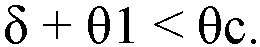
- In a preferable embodiment, the light emission angle δ of the optical film, the first included angle θ1 of the light control film, and the critical angle θc of the light control film satisfy the following relationship: δ + θ1 < θc.
- In a preferable embodiment, the optical film is a louver film with multiple blocking sections spaced along the first direction and multiple light-transmitting sections located between adjacent blocking sections. Each of the first optical structures extends along a second direction, wherein the first direction is not parallel to the second direction, and each of the blocking sections and each of the light-transmitting sections extend along the second direction.
- In a preferable embodiment, the backlight module further includes a prism positioned between the surface light source and the optical film, and the prism has multiple strip-shaped microstructures extending along the first direction.
- In a preferable embodiment, the backlight module further includes a prism positioned between the surface light source and the optical film, each of the first optical structures extends along a second direction, wherein the first direction is not parallel to the second direction, and the prism has multiple strip-shaped microstructures extending along the second direction.
- In a preferable embodiment, the light control film further includes a second reference surface opposite to the first reference surface and multiple second optical structures arranged along the first direction on the second reference surface. Each of the first optical structures extends along a second direction, wherein the first direction is not parallel to the second direction. Each of the second optical structures extends along the second direction. Each of the second optical structures includes a third optical surface and a fourth optical surface. A third included angle θ3 is formed between the third optical surface and the second reference surface, a fourth included angle θ4 is formed between the fourth optical surface and the second reference surface, and the third included angle θ3 is acute and smaller than the fourth included angle θ4.
- In a preferable embodiment, the light emission angle δ of the optical film, the first included angle θ1 of the light control film, the third included angle θ3, and the critical angle θc of the light control film satisfy the following relationship:

- In a preferable embodiment, the first included angle θ1 of the first optical structure and the third included angle θ3 of the second optical structure are oriented towards the same side of the light control film. Both the first included angle θ1 and the third included angle θ3 are less than 45 degrees, and both the second included angle θ2 and the fourth included angle θ4 are greater than 45 degrees.
- In a preferable embodiment, the first included angle θ1 is greater than the third included angle θ3.
- In a preferable embodiment, the surface light source includes a light guide plate and a light bar. The light guide plate has a light incident side and a light exit side connected to the light incident side. The light bar is positioned on the light incident side of the light guide plate, and the light exit side faces the optical film.
- In a preferable embodiment, the light bar includes a circuit board and multiple light-emitting elements, the circuit board extends along the first direction, and the light-emitting elements are arranged along the first direction.
- In a preferable embodiment, the surface light source includes a circuit board parallel to the optical film and multiple light-emitting elements positioned on the circuit board.
- In a preferable embodiment, the surface light source further includes a diffusion plate, which has a bottom surface and a top surface opposite to the bottom surface, the bottom surface faces the circuit board, and the top surface faces the optical film.
- Another object of the present invention is to provide a display device which includes the backlight module as described above, and a display panel arranged on the backlight module.
- The characteristic of the present invention is that due to the asymmetrical nature of the first prism structure in the light control film, light passing through the film is deflected to one side by its asymmetrical microstructure, thereby suppressing the transmittance on the other side. As a result, when applied to displays such as the Driver Information Display (DID) or Co-Driver Display (CDD) positioned in front of the driver's or co-driver's seat, the light distribution can be biased to one side, making it less susceptible to reflection from the left-side or right-side windows.
- In order to illustrate the embodiments and their advantages more fully, the following description is now made with reference to the accompanying drawings.
-
FIG. 1 is a three-dimensional exploded diagram illustrating a first preferred embodiment of the backlight module of this present invention, wherein a light source is a side-lit light source. -
FIG. 2 is side-view diagram illustrating another angle ofFIG. 1 . -
FIG. 3 is a partial enlarged diagram illustrating the structure of a light control film of the first embodiment. -
FIG. 4 is a light field distribution diagram illustrating the light field distribution without using the light control film of the present invention. -
FIG. 5 is a light field distribution diagram illustrating the light field distribution when the microstructure of the light control film and the microstructure of an optical film are perpendicular to each other. -
FIG. 6 is a light field distribution diagram illustrating the light field distribution in which the microstructure of the light control film and the microstructure of the optical film are parallel to each other, and the microstructure of the prism and the microstructure of the light control film are perpendicular to each other. -
FIG. 7 is a three-dimensional exploded diagram illustrating the microstructure of the light control film, the microstructure of the optical film, and the microstructure of the prism are parallel to each other. -
FIG. 8 is a light field distribution diagram illustrating the light field distribution formed by the structure ofFIG. 7 . -
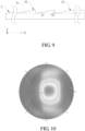
FIG. 9 is a partially enlarged diagram illustrating the partial structure of the light control film in the second preferred embodiment of the backlight module of this present invention. -
FIG. 10 is a light field distribution diagram illustrating the light field distribution formed by the structure ofFIG.9 . -
FIG. 11 is a three-dimensional exploded diagram illustrating another form of the first preferred embodiment, wherein a light source is a direct-lit light source. -
FIG. 12 is a three-dimensional exploded diagram illustrating a third preferred embodiment of the backlight module of this present invention. -
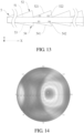
FIG. 13 is a partially enlarged diagram illustrating the partial structure of the light control film in the third preferred embodiment of the backlight module of this present invention. -
FIG. 14 is a light field distribution diagram illustrating the light field distribution formed by the structure ofFIG. 13 . -
FIG. 15 is a graph that quantifies the light field distribution values of various embodiments. -
FIG. 16 is a graph illustrating the numerical difference in light field distribution between using the light control film alone and using the light control film in conjunction with the optical film. -
FIG. 17 is a graph illustrating the light transmittance by using this optical film. -
FIG. 18 is a graph illustrating the numerical difference in light field distribution between using the light control film alone and using the light control film in conjunction with the optical film. -
FIG. 19 is a graph illustrating the numerical difference in light field distribution between the light control film with a single-sided microstructure and a double-sided microstructure. -
FIG. 20 is a schematic diagram illustrating the light deflection range of the backlight module of the present invention when used in vehicle-mounted equipment. - The detailed description and preferred embodiments of the invention will be set forth in the following content and provided for people skilled in the art to understand the characteristics of the invention.
- The light field distribution diagram disclosed in the present invention is obtained by observing the brightness level of the 360-degree direction of the light-emitting surface (perpendicular to the light-emitting plane) from the normal direction of the backlight module. Therefore, the light field distribution diagram is a circle, and the scale around the circle is an angle. The scales marked on each concentric circle inside represent the tilt angle between the viewing direction and the normal direction of the backlight module.
- Secondly, the words "about", "slightly", "approximately" or "substantially" appearing in the content of this case not only cover the clearly stated numerical values and numerical ranges, but also covers the allowable deviation range that can be understood by a person with ordinary knowledge in the technical field to which the invention belongs. The deviation range can be determined by the error generated during measurement, and this error is caused, for example, by limitations of the measurement system or process conditions. In addition, "about" may mean within one or more standard deviations of the above numerical value, such as within ±5%, ±3%, or ±1%. Words such as "about", "slightly", "approximately" or "substantially" appearing in this text may be used to select acceptable deviation ranges or standard deviations based on optical properties, etching properties, mechanical properties, or other properties. Therefore, a single standard deviation is not applied to all the above optical properties, etching properties, mechanical properties, and other properties.
- Referring to
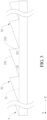
FIG. 1 andFIG. 2 , it is a first preferred embodiment of the backlight module of the present invention. The backlight module includes a surfacelight source 2, aprism 3, anoptical film 4, and alight control film 5. A display panel (not shown) is provided in the light emitting direction of thelight control film 5 to form a display device. - The
optical film 4 is defined to have a first direction X, and a second direction Y that is not parallel to the first direction X. In this embodiment, the second direction Y is perpendicular to the first direction. X, but it is not limited to this. In this embodiment, theoptical film 4 is a louver film and has a plurality of blockingsections 41 spaced apart along the first direction X, and a plurality of light-transmittingsections 42 located between adjacent blockingsections 41. Each of the blockingsections 41 and the light-transmittingsections 42 extends along the second direction Y. In other embodiments, theoptical film 4 may be a light-transmitting film having a prism structure or a light splitting structure instead of a louver film, so the description of this embodiment should not be limited. - Referring to
FIG. 2 andFIG.3 , thelight control film 5 has afirst reference surface 51 facing away from theoptical film 4, and a plurality of firstoptical structures 52 disposed on thefirst reference surface 51 along the first direction X. Each of the firstoptical structures 52 extends along the second direction Y. That is to say, the blockingsections 41 and the light-transmittingsections 42 of theoptical film 4 are arranged parallel to the firstoptical structures 52 of thelight control film 5. Each of the firstoptical structures 52 has a firstoptical surface 521 and a secondoptical surface 522. In this embodiment, the firstoptical surface 521, the secondoptical surface 522, and thefirst reference surface 51 together form a triangle, so that each firstoptical structure 52 has a triangular cross-section. However, in other embodiments, one or both of the firstoptical surface 521 and the secondoptical surface 522 can be designed as a compound slope, without causing each firstoptical structure 52 to have a triangular cross-section. It should not be limited to the description of this embodiment. As shown inFIG. 3 , the firstoptical surface 521 and the secondoptical surface 522 are arranged along the first direction X. The firstoptical surface 521 and thefirst reference surface 51 form a first included angle θ1, and the secondoptical surface 522 and thefirst reference surface 51 form a second included angle θ2. The first included angle θ1 is an acute angle, and the first included angle θ1 is smaller than the second included angle θ2. In the first preferred embodiment of the present invention, the first included angle θ1 is 20°, and the second included angle θ2 is 80°. Therefore, each firstoptical structure 52 has a triangular cross-section in which the first included angle θ1 and the second included angle θ2 are angularly asymmetric. - The
optical film 4 disclosed in this embodiment is used to change the light field distribution of thesurface light source 2 to a single direction first. Then, the firstoptical structure 52 of thelight control film 5 extending in the same direction as the blockingportion 41 of theoptical film 4 is used to adjust the light field distribution that has become a single direction. Since each of the firstoptical structures 52 of thelight control film 5 has an angularly asymmetric microstructure in which the first included angle θ1 is smaller than the second included angle θ2, therefore, when light passes through thelight control film 5, its angularly asymmetric microstructure will effectively deflect and guide the light to a specific side for light extraction, while effectively suppressing the light extraction efficiency on the other side. As a result, when applied to displays such as the Driver Information Display (DID) or Co-Driver Display (CDD) positioned in front of the driver's or co-driver's seat, the light distribution can be biased to one side, making it less susceptible to reflection from the left- side or right-side windows. - As shown in
FIG. 4 , it is a light field distribution diagram without using thelight control film 5 of the present invention. The dark area is in the center and does not produce any offset effect. In addition, as shown inFIG. 5 , even if thelight control film 5 of the present invention is used, the extending direction of the firstoptical structure 52 of thelight control film 5 and the extending direction of the blockingportion 41 and the light-transmittingportion 42 of theoptical film 4 are perpendicular to each other, and the offset effect is still unable to be produced, and a large amount of noise will be generated on both sides. Therefore, as shown inFIG. 1 , the present invention must use thelight control film 5 and theoptical film 4 at the same time, and the extending direction of the firstoptical structure 52 of thelight control film 5 and the extending direction of the blockingportion 41 and the light-transmittingportion 42 of theoptical film 4 must be parallel to each other. In this way, as shown inFIG. 6 , the dark area can be deviated from the center, producing the required offset effect. - It should be noted that, the
prism 3 is between thesurface light source 2 and theoptical film 4 to assist in converging the light field distribution of thesurface light source 2, so that the light can enter theoptical film 4 above theprism 3 in a more concentrated manner to avoid loss of light energy or brightness. In addition, theprism 3 has a plurality of strip-shapedmicrostructures 31, and the strip-shapedmicrostructures 31 may extend along the first direction X as shown inFIG. 1 . The corresponding light field distribution is shown inFIG. 6 , which can produce a good offset effect. The strip-shapedmicrostructure 31 may also extend along the second direction Y as shown inFIG. 7 , and its corresponding light field distribution is shown inFIG. 8 , which can also produce a good offset effect. ComparingFIG. 6 and FIG. 8 , the extending direction of the strip-shapedmicrostructures 31 of theprism 3 will not affect the offset effect. - Referring to
FIG. 9 , which is a second preferred embodiment of the backlight module of the present invention. The difference from the first preferred embodiment is that the first included angle of thelight control film 5 is less than 45 degrees, and the second included angle is a right angle. InFIG. 9 , the first included angle θ1 is 10°, and the second included angle θ2 is 90°, so that each of the firstoptical structures 52 has a right-angled triangle cross-section. However, the second included angle θ2 may also be an acute angle to improve the problem of difficulty in mold release at right angles. The light field distribution diagram inFIG. 10 shows that offset effects can also be produced. Compared withFIG. 6 ,FIG. 10 shows that there are significantly fewer light-colored striped areas on the left, which means that energy or brightness loss can be effectively reduced and better offset effects can be obtained. - Referring to
FIG. 1 andFIG.2 , in the first preferred embodiment, thesurface light source 2 is side-lit light source and includes alight guide plate 21, adiffusion film 22, and alight bar 23. Thelight guide plate 21 has alight incident side 211 and alight exit side 212 connected to thelight incident side 211. Thediffusion film 22 is disposed on thelight exit side 212 of thelight guide plate 21. Thelight bar 23 is disposed on thelight incident side 211 of thelight guide plate 21, and thelight exit side 212 faces theoptical film 4. Thelight bar 23 has a circuit board 231 (not shown inFIG. 2 ) and a plurality of light-emittingelements 232. Thecircuit board 231 extends along the first direction X, and the light-emittingelements 232 are arranged along the first direction X. Therefore, the extending direction of thecircuit board 231 and the arrangement direction of the light-emittingelements 232 are different from the extending directions of the blockingportion 41 of theoptical film 4 and the firstoptical structure 52 of thelight control film 5. In this embodiment, they are perpendicular to each other. In this way, the light can be effectively deflected and guided to a specific side, while the light efficiency on the other side can be effectively suppressed. On the contrary, if the extending direction of thecircuit board 231 and the arrangement direction of the light-emittingelements 232 are the same as the extending directions of the blockingsections 41 of theoptical film 4 and the firstoptical structures 52 of thelight control film 5, the light emission on the other side cannot be suppressed. - Furthermore, the
surface light source 2 may also be a direct-lit light source as shown inFIG. 11 , including acircuit board 231 parallel to theoptical film 4, a plurality oflight emitting elements 232 arranged on thecircuit board 231, and adiffusion plate 24. Thediffusion plate 24 has abottom surface 241 and atop surface 242 opposite to thebottom surface 241. Thebottom surface 241 faces thecircuit board 231, and thetop surface 242 faces theoptical film 4. In the present invention, thesurface light source 2 can be either side-lit light source or direct-lit light source. - Referring to
FIG. 12 , a third preferred embodiment of the backlight module of the present invention. The backlight module includes alight source 2, aprism 3, anoptical film 4, and alight control film 5. The difference from the first preferred embodiment is that thelight control film 5 further includes a plurality ofoptical structures 54 facing theoptical film 4 and disposed along the first direction X. Each of the firstoptical structures 52 and the secondoptical structures 54 extends along the second direction Y. - Referring to
FIG. 13 , in more detail, thelight control film 5 further includes asecond reference surface 53 opposite to thefirst reference surface 51 and facing theoptical film 4. The secondoptical structures 54 are disposed on thesecond reference surface 53 along the first direction X. Each of the firstoptical structures 52 has a firstoptical surface 521 and a secondoptical surface 522. The firstoptical surface 521 and thefirst reference surface 51 have a first included angle θ1, and the secondoptical surface 522 and thefirst reference surface 51 have a second included angle θ2. The first included angle θ1 is an acute angle, and the first included angle θ1 is smaller than the second included angle θ2. Each of the secondoptical structures 54 has a thirdoptical surface 541 and a fourthoptical surface 542. The thirdoptical surface 541 and thesecond reference surface 53 form a third included angle θ3, and the fourthoptical surface 542 and thesecond reference surface 53 form a fourth included angle θ4. The third included angle θ3 is an acute angle, and the third included angle θ3 is smaller than the fourth included angle θ4. The first included angle θ1 of the firstoptical structures 52 and the third included angle θ3 of the secondoptical structures 54 are oriented towards the same side of thelight control film 5. The first included angle θ1 and the third included angle θ3 are both less than 45 degrees, and the second included angle θ2 and the fourth included angle θ4 are both greater than 45 degrees. The first included angle θ1 is greater than the third included angle θ3, the fourth included angle θ4 is greater than the second included angle θ2, and the fourth included angle θ4 is a right angle. In this embodiment, the first included angle θ1 is 20°, the second included angle θ2 is 80°, the third included angle θ3 is 10°, and the fourth included angle θ4 is 90°. The light field distribution diagram inFIG. 14 can also produce an offset effect, and compared withFIG. 6 , the dark area inFIG. 14 is located further away from the center, resulting in more obvious offset effect. In short, compared with the firstoptical structures 52 being provided on only one side of thelight control film 5, this embodiment uses thelight control film 5 with the secondoptical structures 54 on thesecond reference surface 53, the light field deflection effect can finely adjust to meet different usage situations or customer requirements. In addition, the firstoptical structures 52 and the secondoptical structures 54 are convex structures. In other embodiments, concave structures may also be used, and their light field deflection effects are still basically the same or similar. Therefore, it should not be limited to the description of this embodiment. - Referring to
FIG. 15 , it is a graph that quantifies the light field distribution values of various embodiments. Wherein, the dotted line represents the control group using only theoptical film 4. The dashed line represents the first preferred embodiment. The dash-dotted line represents the second preferred embodiment. The solid line represents the third preferred embodiment.FIG. 15 shows that compared with the control group, the third preferred embodiment can most effectively suppress the light output at the viewing angle of -30° to -15°and shift the light output to the viewing angle of 15° to 30°, which can effectively suppress the light extraction of one side and produce an offset effect. It should be noted that each included angle of thelight control film 5 may be adjusted to adjust the light deflection range according to different application environments to obtain the best offset effect. - In the first preferred embodiment of the backlight module of the present invention, the
light control film 5 is arranged so that after the light passes through and leaves thelight control film 5, it is deflected in a direction away from the firstoptical surface 521. In this way, the light is deflected to one side and the light emission of the other side is suppressed, so the backlight module can be applied to the environments that require asymmetric light fields. However, if there is only thelight control film 5 but no theoptical film 4, there will still be significant stray light in the viewing angle distribution in the horizontal between ±60 and ±90 degrees, as shown inFIG. 16 . In order to eliminate large-angle stray light caused by total reflection, the first preferred embodiment of the backlight module of the present invention also needs to dispose theoptical film 4 between thelight control film 5 and thesurface light source 2. In this way, the light that is prone to total reflection in the light control film 5 (that is, the light with an incident angle greater than the critical angle θc of the light control film 5) is eliminated (or cut-off) before entering thelight control film 5. InFIG. 16 , the dotted line represents the control group using only thelight control film 5. The dashed line represents the first preferred embodiment. As shown inFIG. 16 , only when thelight control film 5 and theoptical film 4 are combined, the light can be deflected to one side and the light emission from the other side can be suppressed. At the same time, it can also avoid the generation of stray light at large angles and significantly reduce the light energy or luminance in the viewing angle area between ±60 and ±90 degrees. - In more detail, the light emission angle δ of the
optical film 4, the first included angle θ1 of thelight control film 5, and the critical angle θc of thelight control film 5 must comply with the following relationship: δ+ θ1 < θc. - Referring to
FIG. 17 , when the light emitted by thesurface light source 2 passes through theoptical film 4, the light emission angle δ is in an angle range relative to the normal direction of the backlight module, and the transmittance is at least 50%. That is, the viewing angle is between approximately -17° to -18° and +24° to +25°. In order to deflect the viewing angle light at negative angles, the value of δ is designed to be 17 in this embodiment. Thelight control film 5 is made of polycarbonate (PC), and its critical angle θc is 39°. Therefore, the first included angle θ1 of thelight control film 5 is designed to be less than 22° to comply with the relationship of δ+θ1<θc. In the first preferred embodiment of the present invention, the first included angle θ1 is 20°, which is less than 22°. In addition, although thelight control film 5 in this embodiment is made of PC, it may also be made of Optically Clear Adhesives (OCA), Polyethylene terephthalate (PET), Poly methyl methacrylate (PMMA). Therefore, the critical angle θc will be different and should not be limited to the description of this embodiment. - Referring to
FIG. 18 , the dotted line represents the control group using only theoptical film 4. The dashed line represents the first preferred embodiment. In this embodiment, when the light leaves thelight control film 5, it is directed away from the firstoptical surface 521 by a deflection angle µ. The angle µ conforms to the following relationship: µ=0.52*θ1+29.7. When the first included angle θ1 is 20°, the deflection angle µ is approximately 40° (0.52* 20°+29.7=40.1°). That is to say, when thelight control film 5 and theoptical film 4 are not combined, the light emitting position of 50% of the light energy or luminance corresponds to a viewing angle of approximately -52° (the dotted line). Compared with the case where thelight control film 5 and theoptical film 4 are combined, the light emitting position of 50% of the light energy or luminance corresponds to a viewing angle of approximately -10° (the dashed line), and the difference between the two is 42°, which is quite close to the above calculation result of the formula. In other embodiments, when the first included angle θ1 is 10°, the deflection angle µ is approximately 35° (0.52* 10°+29.7=34.9°). When the first included angle θ1 is 40°, the deflection angle µ is approximately 50° (0.52* 40°+29.7=50.5°). In other embodiments, when the first included angle θ1 is 10°, the deflection angle µ is approximately 35° (0.52*10°+29.7=34.9°). When the first included angle θ1 is 40°, the deflection angle µ is approximately 50° (0.52* 40°+29.7=50.5°). Therefore, the above formula can effectively represent the relationship between the deflection angle µ and the first included angle θ1. - When the
light control film 5 is adopted as a double-sided microstructure similar to the third preferred embodiment of the backlight module of the present invention, the light emission angle δ of theoptical film 4, the first included angle θ1 of thelight control film 5, the third included angle θ3, and the critical angle θc of thelight control film 5 must meet the following formula: δ+(θ1+θ3)<θc. Referring toFIG. 19 , when thelight control film 5 with single-sided microstructures has the first internal angle θ1 of 20° (the dashed line), the light emitting position of 50% of the light energy or luminance corresponds to a viewing angle of approximately -10°. When thelight control film 5 with double-sided microstructures has the first internal angle θ1 of 10° and the third included angle θ3 of 10° (the solid line), the light emitting position of 50% of the light energy or luminance also corresponds to a viewing angle of approximately -10°. Both the single-sided microstructures of the first preferred embodiment and the double-sided microstructures of the third preferred embodiment can deflect light to one side and suppress the light extraction of the other side. At the same time, they can also avoid large-angle stray light. Wherein, the double-sided microstructures of the third preferred embodiment can further reduce the energy or luminance at viewing angles between -30° to -60° and +70° to +90°. - Through the above design, when the backlight module of the present invention is used in vehicle-mounted equipment, as shown in
FIG. 20(a) , the image of thedashboard 91 located on the driver's seat side can be projected to the driver's seat and passenger seat, and it will not be reflected by the window on the driver's side. Alternatively, as shown inFIG. 20(b) , the image of thedisplay screen 92 located on the passenger's seat side can be projected to the driver's seat and the passenger's seat but will not be reflected by the window on the passenger's side, reducing interference caused by image reflections. - To sum up, the backlight module of the present invention can deflect light to one side and suppress the light emission rate of the other side through the combination of the optical film and the light control film, and it can be applied to environments that require anisotropic light fields.
- Although the present invention has been described in considerable detail with reference to certain embodiments thereof, other embodiments are possible. Therefore, the spirit and scope of the appended claims should not be limited to the description of the embodiments contained herein.
- It will be apparent to those skilled in the art that various modifications and variations can be made to the structure of the present invention without departing from the scope or spirit of the invention. In view of the foregoing, it is intended that the present invention cover modifications and variations of this invention provided they fall within the scope of the following claims.
-
- 2
- surface light source
- 21
- light guide plate
- 211
- light incident side
- 212
- light exit side
- 22
- diffusion film
- 23
- light bar
- 231
- circuit board
- 232
- light-emitting element
- 24
- diffusion plate
- 241
- bottom surface
- 242
- top surface
- 3
- prism
- 31
- strip-shaped microstructure
- 4
- optical film
- 41
- blocking section
- 42
- light-transmitting section
- 5
- light control film
- 51
- first reference surface
- 52
- first optical structure
- 521
- first optical surface
- 522
- second optical surface
- 53
- second reference surface
- 54
- second optical structure
- 541
- third optical surface
- 542
- fourth optical surface
- 91
- dashboard
- 92
- display screen
- X
- first direction
- Y
- second direction
- θ1
- first included angle
- θ2
- second included angle
- θ3
- third included angle
- θ4
- fourth included angle
Claims (16)
- A backlight module, comprising:a surface light source;an optical film, disposed on an emitting side of the surface light source; anda light control film, comprising a first reference surface and multiple first optical structures positioned on the first reference surface, wherein the first reference surface is located on a side of the light control film facing away from the optical film, each of said first optical structures comprises a first optical surface and a second optical surface, wherein the first optical surface and the second optical surface are arranged along a first direction, a first included angle θ1 is formed between the first optical surface and the first reference surface, a second included angle θ2 is formed between the second optical surface and the first reference surface, the first included angle θ1 is an acute angle, and the first included angle θ1 is smaller than the second included angle θ2.
- The backlight module as claimed in claim 1, wherein the light emitted by the surface light source has a light emission angular range of δ relative to the normal direction of the backlight module when passing through the optical film, the transmittance of the light is at least 50%, and the light deflects in a direction away from the first optical surface after entering the light control film.
- The backlight module as claimed in claim 2, wherein the light deflects at an angle µ in the direction away from the first optical surface of the light control film when it exits the light control film, and the angle µ is determined by the following relationship: µ = 0.52*θ1 + 29.7.
- The backlight module as claimed in claim 2, wherein the light emission angle δ of the optical film, the first included angle θ1 of the light control film, and the critical angle θc of the light control film satisfy the following relationship:
- The backlight module as claimed in claim 1, wherein the optical film is a louver film with multiple blocking sections spaced along the first direction and multiple light-transmitting sections located between adjacent blocking sections, each of the first optical structures extends along a second direction, wherein the first direction is not parallel to the second direction, and each of the blocking sections and each of the light-transmitting sections extend along the second direction.
- The backlight module as claimed in claim 1, wherein the backlight module further comprises a prism positioned between the surface light source and the optical film, and the prism has multiple strip-shaped microstructures extending along the first direction.
- The backlight module as claimed in claim 1, wherein the backlight module further comprises a prism positioned between the surface light source and the optical film, each of the first optical structures extends along a second direction, wherein the first direction is not parallel to the second direction, and the prism has multiple strip-shaped microstructures extending along the second direction.
- The backlight module as claimed in claim 1, wherein the light control film further comprises a second reference surface opposite to the first reference surface and multiple second optical structures arranged along the first direction on the second reference surface, each of the first optical structures extends along a second direction, wherein the first direction is not parallel to the second direction, each of the second optical structures extends along the second direction, each of the second optical structures comprises a third optical surface and a fourth optical surface, a third included angle θ3 is formed between the third optical surface and the second reference surface, a fourth included angle θ4 is formed between the fourth optical surface and the second reference surface, and the third included angle θ3 is acute and smaller than the fourth included angle θ4.
- The backlight module as claimed in claim 8, wherein the light emission angle δ of the optical film, the first included angle θ1 of the light control film, the third included angle θ3, and the critical angle θc of the light control film satisfy the following relationship: δ + (θ1 + θ3) < θc.
- The backlight module as claimed in claim 8, wherein the first included angle θ1 of the first optical structure and the third included angle θ3 of the second optical structure are oriented towards the same side of the light control film, both the first included angle θ1 and the third included angle θ3 are less than 45 degrees, and both the second included angle θ2 and the fourth included angle θ4 are greater than 45 degrees.
- The backlight module as claimed in claim 8, wherein the first included angle θ1 is greater than the third included angle θ3.
- The backlight module as claimed in any one of claims 1 to 11, wherein the surface light source comprises a light guide plate and a light bar, the light guide plate has a light incident side and a light exit side connected to the light incident side, the light bar is positioned on the light incident side of the light guide plate, and the light exit side faces the optical film.
- The backlight module as claimed in claim 12, wherein the light bar comprises a circuit board and multiple light-emitting elements, the circuit board extends along the first direction, and the light-emitting elements are arranged along the first direction.
- The backlight module as claimed in any one of claims 1 to 11, wherein the surface light source comprises a circuit board parallel to the optical film and multiple light-emitting elements positioned on the circuit board.
- The backlight module as claimed in claim 14, wherein the surface light source further comprises a diffusion plate, which has a bottom surface and a top surface opposite to the bottom surface, the bottom surface faces the circuit board, and the top surface faces the optical film.
- A display device, comprising the backlight module as claimed in any one of claims 1 to 15, and a display panel arranged on the backlight module.
Applications Claiming Priority (2)
| Application Number | Priority Date | Filing Date | Title |
|---|---|---|---|
| CN202210460207 | 2022-04-28 | ||
| PCT/CN2023/090823 WO2023208035A1 (en) | 2022-04-28 | 2023-04-26 | Backlight module and display device |
Publications (2)
| Publication Number | Publication Date |
|---|---|
| EP4517418A1 true EP4517418A1 (en) | 2025-03-05 |
| EP4517418A4 EP4517418A4 (en) | 2025-08-27 |
Family
ID=87803043
Family Applications (1)
| Application Number | Title | Priority Date | Filing Date |
|---|---|---|---|
| EP23795467.2A Pending EP4517418A4 (en) | 2022-04-28 | 2023-04-26 | BACKLIGHT MODULE AND DISPLAY DEVICE |
Country Status (7)
| Country | Link |
|---|---|
| US (2) | US12468082B2 (en) |
| EP (1) | EP4517418A4 (en) |
| JP (1) | JP2025514351A (en) |
| KR (1) | KR20250004008A (en) |
| CN (1) | CN117940841A (en) |
| TW (2) | TWI805464B (en) |
| WO (2) | WO2023206858A1 (en) |
Family Cites Families (20)
| Publication number | Priority date | Publication date | Assignee | Title |
|---|---|---|---|---|
| US6166787A (en) * | 1998-03-17 | 2000-12-26 | Motorola, Inc. | Optical display device having prismatic film for enhanced viewing |
| JP2001195913A (en) * | 2000-01-07 | 2001-07-19 | Toshiba Corp | Flat panel display backlight |
| WO2005017581A2 (en) * | 2003-08-15 | 2005-02-24 | Koninklijke Philips Electronics N.V. | Backlight device |
| EP2168004A2 (en) * | 2007-06-22 | 2010-03-31 | 3M Innovative Properties Company | Systems and methods for controlling backlight output characteristics |
| JP5011009B2 (en) * | 2007-07-06 | 2012-08-29 | 株式会社ジャパンディスプレイイースト | Liquid crystal display |
| JP5184707B1 (en) * | 2012-03-30 | 2013-04-17 | 株式会社ナナオ | Liquid crystal display |
| TWI481932B (en) * | 2012-06-26 | 2015-04-21 | Au Optronics Corp | Display device and display system combined thereof |
| CN102879942A (en) * | 2012-06-26 | 2013-01-16 | 友达光电股份有限公司 | Display device and combined display system |
| TW201407199A (en) * | 2012-08-15 | 2014-02-16 | 財團法人工業技術研究院 | Light deflecting film |
| KR102078025B1 (en) * | 2013-09-25 | 2020-02-18 | 엘지디스플레이 주식회사 | Optical sheet and liquid crystal display device having the same |
| JP7205463B2 (en) * | 2017-03-31 | 2023-01-17 | 大日本印刷株式会社 | Optical sheet, light control member, surface light source device, image source unit, and display device |
| WO2019045095A1 (en) * | 2017-09-04 | 2019-03-07 | 富士フイルム株式会社 | Backlight unit and liquid crystal display device |
| TWI725727B (en) * | 2020-02-05 | 2021-04-21 | 瑞儀光電股份有限公司 | Backlight module and method for adjusting viewing angle of display |
| CN111474624A (en) * | 2020-05-27 | 2020-07-31 | 京东方科技集团股份有限公司 | Backlight structure and LCD display module |
| CN111580308A (en) * | 2020-07-03 | 2020-08-25 | 上海天马微电子有限公司 | Backlight module and display device |
| CN112666752A (en) * | 2020-12-28 | 2021-04-16 | 深圳创维汽车智能有限公司 | Backlight module assembly, liquid crystal display and automobile |
| JP2023117649A (en) * | 2022-02-14 | 2023-08-24 | 船井電機株式会社 | Mobile-mounted display device |
| JP7504141B2 (en) * | 2022-02-28 | 2024-06-21 | シャープディスプレイテクノロジー株式会社 | Illumination and display devices |
| CN217386004U (en) * | 2022-03-08 | 2022-09-06 | 瑞仪光电股份有限公司 | Optical diaphragm, backlight module, display and lamp |
| CN218064734U (en) * | 2022-04-28 | 2022-12-16 | 瑞仪光电股份有限公司 | Backlight module and display device |
-
2022
- 2022-08-10 TW TW111129990A patent/TWI805464B/en active
- 2022-08-10 WO PCT/CN2022/111525 patent/WO2023206858A1/en not_active Ceased
-
2023
- 2023-04-26 JP JP2024563704A patent/JP2025514351A/en active Pending
- 2023-04-26 CN CN202380013249.3A patent/CN117940841A/en active Pending
- 2023-04-26 EP EP23795467.2A patent/EP4517418A4/en active Pending
- 2023-04-26 KR KR1020247039549A patent/KR20250004008A/en active Pending
- 2023-04-26 WO PCT/CN2023/090823 patent/WO2023208035A1/en not_active Ceased
- 2023-04-26 TW TW112115531A patent/TWI848673B/en active
-
2024
- 2024-10-25 US US18/927,724 patent/US12468082B2/en active Active
-
2025
- 2025-10-03 US US19/349,012 patent/US20260029567A1/en active Pending
Also Published As
| Publication number | Publication date |
|---|---|
| TWI848673B (en) | 2024-07-11 |
| CN117940841A (en) | 2024-04-26 |
| JP2025514351A (en) | 2025-05-02 |
| KR20250004008A (en) | 2025-01-07 |
| WO2023208035A1 (en) | 2023-11-02 |
| US20260029567A1 (en) | 2026-01-29 |
| US12468082B2 (en) | 2025-11-11 |
| TWI805464B (en) | 2023-06-11 |
| TW202343109A (en) | 2023-11-01 |
| TW202343110A (en) | 2023-11-01 |
| WO2023206858A1 (en) | 2023-11-02 |
| EP4517418A4 (en) | 2025-08-27 |
| US20250044495A1 (en) | 2025-02-06 |
Similar Documents
| Publication | Publication Date | Title |
|---|---|---|
| KR100681220B1 (en) | Planar light source device and display device | |
| US20110255305A1 (en) | Multi-layer light guide apparatus | |
| US20070165419A1 (en) | Spread illuminating apparatus having light reflecting sheet with light diffusing portions | |
| US7452118B2 (en) | Area light source | |
| KR20110135798A (en) | Surface light source device and stereoscopic display device | |
| CN102588766B (en) | Light-emitting device and image display | |
| CN113238408B (en) | Display device | |
| EP2523024A1 (en) | Backlight unit and liquid crystal module | |
| US20170115447A1 (en) | Prism sheet and planar illumination device | |
| US7780331B2 (en) | Surface illuminant equipment | |
| CN215867450U (en) | Backlight module and display device | |
| US12271019B2 (en) | Backlight module | |
| EP4517418A1 (en) | Backlight module and display device | |
| CN218064734U (en) | Backlight module and display device | |
| US9304242B2 (en) | Display device | |
| JP2007163627A (en) | Illumination device, electro-optical device and electronic apparatus | |
| JP2017208287A (en) | Surface light source device and transmission type display device | |
| JP2020013067A (en) | Optical structure and display device | |
| JP5929552B2 (en) | Light guide plate, surface light source device, transmissive display device | |
| US12282632B2 (en) | Infrared touch screen for reducing touch height of touch panel | |
| CN119487442A (en) | Backlight module and display device | |
| US20260023206A1 (en) | Light guide for a backlight, backlight and display device | |
| CN221804437U (en) | Display device | |
| CN223966715U (en) | Abnormal light guide plate with groove design, backlight module and display device | |
| CN221426892U (en) | Cornea transferring, backlight module and liquid crystal display device |
Legal Events
| Date | Code | Title | Description |
|---|---|---|---|
| STAA | Information on the status of an ep patent application or granted ep patent |
Free format text: STATUS: THE INTERNATIONAL PUBLICATION HAS BEEN MADE |
|
| PUAI | Public reference made under article 153(3) epc to a published international application that has entered the european phase |
Free format text: ORIGINAL CODE: 0009012 |
|
| STAA | Information on the status of an ep patent application or granted ep patent |
Free format text: STATUS: REQUEST FOR EXAMINATION WAS MADE |
|
| 17P | Request for examination filed |
Effective date: 20241127 |
|
| AK | Designated contracting states |
Kind code of ref document: A1 Designated state(s): AL AT BE BG CH CY CZ DE DK EE ES FI FR GB GR HR HU IE IS IT LI LT LU LV MC ME MK MT NL NO PL PT RO RS SE SI SK SM TR |
|
| DAV | Request for validation of the european patent (deleted) | ||
| DAX | Request for extension of the european patent (deleted) | ||
| A4 | Supplementary search report drawn up and despatched |
Effective date: 20250729 |
|
| RIC1 | Information provided on ipc code assigned before grant |
Ipc: G02F 1/13357 20060101AFI20250723BHEP Ipc: F21V 5/02 20060101ALI20250723BHEP Ipc: F21V 8/00 20060101ALI20250723BHEP |