JP7205463B2 - Optical sheet, light control member, surface light source device, image source unit, and display device - Google Patents
Optical sheet, light control member, surface light source device, image source unit, and display device Download PDFInfo
- Publication number
- JP7205463B2 JP7205463B2 JP2019509396A JP2019509396A JP7205463B2 JP 7205463 B2 JP7205463 B2 JP 7205463B2 JP 2019509396 A JP2019509396 A JP 2019509396A JP 2019509396 A JP2019509396 A JP 2019509396A JP 7205463 B2 JP7205463 B2 JP 7205463B2
- Authority
- JP
- Japan
- Prior art keywords
- light
- optical
- layer
- optical sheet
- optical element
- Prior art date
- Legal status (The legal status is an assumption and is not a legal conclusion. Google has not performed a legal analysis and makes no representation as to the accuracy of the status listed.)
- Active
Links
Images


Classifications
-
- G—PHYSICS
- G02—OPTICS
- G02B—OPTICAL ELEMENTS, SYSTEMS OR APPARATUS
- G02B3/00—Simple or compound lenses
- G02B3/02—Simple or compound lenses with non-spherical faces
- G02B3/08—Simple or compound lenses with non-spherical faces with discontinuous faces, e.g. Fresnel lens
-
- G—PHYSICS
- G02—OPTICS
- G02F—OPTICAL DEVICES OR ARRANGEMENTS FOR THE CONTROL OF LIGHT BY MODIFICATION OF THE OPTICAL PROPERTIES OF THE MEDIA OF THE ELEMENTS INVOLVED THEREIN; NON-LINEAR OPTICS; FREQUENCY-CHANGING OF LIGHT; OPTICAL LOGIC ELEMENTS; OPTICAL ANALOGUE/DIGITAL CONVERTERS
- G02F1/00—Devices or arrangements for the control of the intensity, colour, phase, polarisation or direction of light arriving from an independent light source, e.g. switching, gating or modulating; Non-linear optics
- G02F1/01—Devices or arrangements for the control of the intensity, colour, phase, polarisation or direction of light arriving from an independent light source, e.g. switching, gating or modulating; Non-linear optics for the control of the intensity, phase, polarisation or colour
- G02F1/13—Devices or arrangements for the control of the intensity, colour, phase, polarisation or direction of light arriving from an independent light source, e.g. switching, gating or modulating; Non-linear optics for the control of the intensity, phase, polarisation or colour based on liquid crystals, e.g. single liquid crystal display cells
- G02F1/133—Constructional arrangements; Operation of liquid crystal cells; Circuit arrangements
- G02F1/1333—Constructional arrangements; Manufacturing methods
- G02F1/1335—Structural association of cells with optical devices, e.g. polarisers or reflectors
- G02F1/133526—Lenses, e.g. microlenses or Fresnel lenses
-
- B—PERFORMING OPERATIONS; TRANSPORTING
- B32—LAYERED PRODUCTS
- B32B—LAYERED PRODUCTS, i.e. PRODUCTS BUILT-UP OF STRATA OF FLAT OR NON-FLAT, e.g. CELLULAR OR HONEYCOMB, FORM
- B32B7/00—Layered products characterised by the relation between layers; Layered products characterised by the relative orientation of features between layers, or by the relative values of a measurable parameter between layers, i.e. products comprising layers having different physical, chemical or physicochemical properties; Layered products characterised by the interconnection of layers
- B32B7/02—Physical, chemical or physicochemical properties
-
- F—MECHANICAL ENGINEERING; LIGHTING; HEATING; WEAPONS; BLASTING
- F21—LIGHTING
- F21S—NON-PORTABLE LIGHTING DEVICES; SYSTEMS THEREOF; VEHICLE LIGHTING DEVICES SPECIALLY ADAPTED FOR VEHICLE EXTERIORS
- F21S2/00—Systems of lighting devices, not provided for in main groups F21S4/00 - F21S10/00 or F21S19/00, e.g. of modular construction
-
- G—PHYSICS
- G02—OPTICS
- G02B—OPTICAL ELEMENTS, SYSTEMS OR APPARATUS
- G02B5/00—Optical elements other than lenses
-
- G—PHYSICS
- G02—OPTICS
- G02B—OPTICAL ELEMENTS, SYSTEMS OR APPARATUS
- G02B5/00—Optical elements other than lenses
- G02B5/02—Diffusing elements; Afocal elements
- G02B5/0205—Diffusing elements; Afocal elements characterised by the diffusing properties
- G02B5/021—Diffusing elements; Afocal elements characterised by the diffusing properties the diffusion taking place at the element's surface, e.g. by means of surface roughening or microprismatic structures
- G02B5/0231—Diffusing elements; Afocal elements characterised by the diffusing properties the diffusion taking place at the element's surface, e.g. by means of surface roughening or microprismatic structures the surface having microprismatic or micropyramidal shape
-
- G—PHYSICS
- G02—OPTICS
- G02B—OPTICAL ELEMENTS, SYSTEMS OR APPARATUS
- G02B5/00—Optical elements other than lenses
- G02B5/04—Prisms
- G02B5/045—Prism arrays
-
- G—PHYSICS
- G02—OPTICS
- G02F—OPTICAL DEVICES OR ARRANGEMENTS FOR THE CONTROL OF LIGHT BY MODIFICATION OF THE OPTICAL PROPERTIES OF THE MEDIA OF THE ELEMENTS INVOLVED THEREIN; NON-LINEAR OPTICS; FREQUENCY-CHANGING OF LIGHT; OPTICAL LOGIC ELEMENTS; OPTICAL ANALOGUE/DIGITAL CONVERTERS
- G02F1/00—Devices or arrangements for the control of the intensity, colour, phase, polarisation or direction of light arriving from an independent light source, e.g. switching, gating or modulating; Non-linear optics
- G02F1/01—Devices or arrangements for the control of the intensity, colour, phase, polarisation or direction of light arriving from an independent light source, e.g. switching, gating or modulating; Non-linear optics for the control of the intensity, phase, polarisation or colour
- G02F1/13—Devices or arrangements for the control of the intensity, colour, phase, polarisation or direction of light arriving from an independent light source, e.g. switching, gating or modulating; Non-linear optics for the control of the intensity, phase, polarisation or colour based on liquid crystals, e.g. single liquid crystal display cells
- G02F1/133—Constructional arrangements; Operation of liquid crystal cells; Circuit arrangements
- G02F1/1333—Constructional arrangements; Manufacturing methods
- G02F1/1335—Structural association of cells with optical devices, e.g. polarisers or reflectors
- G02F1/133504—Diffusing, scattering, diffracting elements
-
- G—PHYSICS
- G02—OPTICS
- G02F—OPTICAL DEVICES OR ARRANGEMENTS FOR THE CONTROL OF LIGHT BY MODIFICATION OF THE OPTICAL PROPERTIES OF THE MEDIA OF THE ELEMENTS INVOLVED THEREIN; NON-LINEAR OPTICS; FREQUENCY-CHANGING OF LIGHT; OPTICAL LOGIC ELEMENTS; OPTICAL ANALOGUE/DIGITAL CONVERTERS
- G02F1/00—Devices or arrangements for the control of the intensity, colour, phase, polarisation or direction of light arriving from an independent light source, e.g. switching, gating or modulating; Non-linear optics
- G02F1/01—Devices or arrangements for the control of the intensity, colour, phase, polarisation or direction of light arriving from an independent light source, e.g. switching, gating or modulating; Non-linear optics for the control of the intensity, phase, polarisation or colour
- G02F1/13—Devices or arrangements for the control of the intensity, colour, phase, polarisation or direction of light arriving from an independent light source, e.g. switching, gating or modulating; Non-linear optics for the control of the intensity, phase, polarisation or colour based on liquid crystals, e.g. single liquid crystal display cells
- G02F1/133—Constructional arrangements; Operation of liquid crystal cells; Circuit arrangements
- G02F1/1333—Constructional arrangements; Manufacturing methods
- G02F1/1335—Structural association of cells with optical devices, e.g. polarisers or reflectors
- G02F1/13356—Structural association of cells with optical devices, e.g. polarisers or reflectors characterised by the placement of the optical elements
- G02F1/133562—Structural association of cells with optical devices, e.g. polarisers or reflectors characterised by the placement of the optical elements on the viewer side
-
- G—PHYSICS
- G02—OPTICS
- G02F—OPTICAL DEVICES OR ARRANGEMENTS FOR THE CONTROL OF LIGHT BY MODIFICATION OF THE OPTICAL PROPERTIES OF THE MEDIA OF THE ELEMENTS INVOLVED THEREIN; NON-LINEAR OPTICS; FREQUENCY-CHANGING OF LIGHT; OPTICAL LOGIC ELEMENTS; OPTICAL ANALOGUE/DIGITAL CONVERTERS
- G02F1/00—Devices or arrangements for the control of the intensity, colour, phase, polarisation or direction of light arriving from an independent light source, e.g. switching, gating or modulating; Non-linear optics
- G02F1/01—Devices or arrangements for the control of the intensity, colour, phase, polarisation or direction of light arriving from an independent light source, e.g. switching, gating or modulating; Non-linear optics for the control of the intensity, phase, polarisation or colour
- G02F1/13—Devices or arrangements for the control of the intensity, colour, phase, polarisation or direction of light arriving from an independent light source, e.g. switching, gating or modulating; Non-linear optics for the control of the intensity, phase, polarisation or colour based on liquid crystals, e.g. single liquid crystal display cells
- G02F1/133—Constructional arrangements; Operation of liquid crystal cells; Circuit arrangements
- G02F1/1333—Constructional arrangements; Manufacturing methods
- G02F1/1335—Structural association of cells with optical devices, e.g. polarisers or reflectors
- G02F1/1336—Illuminating devices
- G02F1/133602—Direct backlight
- G02F1/133606—Direct backlight including a specially adapted diffusing, scattering or light controlling members
- G02F1/133607—Direct backlight including a specially adapted diffusing, scattering or light controlling members the light controlling member including light directing or refracting elements, e.g. prisms or lenses
Landscapes
- Physics & Mathematics (AREA)
- Nonlinear Science (AREA)
- Optics & Photonics (AREA)
- General Physics & Mathematics (AREA)
- Crystallography & Structural Chemistry (AREA)
- Chemical & Material Sciences (AREA)
- Mathematical Physics (AREA)
- Engineering & Computer Science (AREA)
- General Engineering & Computer Science (AREA)
- Optical Elements Other Than Lenses (AREA)
- Planar Illumination Modules (AREA)
- Liquid Crystal (AREA)
- Devices For Indicating Variable Information By Combining Individual Elements (AREA)
- Laminated Bodies (AREA)
Description
本発明は、入射した光の出射方向を制御する光学シート、並びにこれを備える光制御部材、面光源装置、映像源ユニット、及び表示装置に関する。 The present invention relates to an optical sheet that controls the direction of emission of incident light, and a light control member, surface light source device, image source unit, and display device having the same.
カーナビゲーション、テレビ、パソコンのモニタ等の表示装置には、表示すべき映像を出射する映像源が備えられるとともに、映像光の質を高めて観察者側に提供するための光学シートが具備されている。 Display devices such as car navigation systems, televisions, and personal computer monitors are equipped with an image source for emitting images to be displayed, and an optical sheet for enhancing the quality of image light and providing it to the observer. there is
映像光の出射方向は正面、又は、正面から上下左右の角度方向とされることが多く、これにより所望の位置から画面に映し出された映像を視認することができる。また、覗き見防止等、必要に応じて出光方向を制限することも行われている。
このように出光角度を制御する光学シートとして例えば特許文献1~特許文献3が開示されている。The direction of emission of the image light is often set to the front, or to the vertical and horizontal directions from the front, so that the image displayed on the screen can be visually recognized from a desired position. In addition, the direction of light emission is restricted as necessary to prevent prying eyes.
近年における機器の多様化により、映像光の出射方向をこれまでとは異なるように、又は、より細かく制御することが必要となってきた。例えばカーナビゲーションについてみると、車内では人が座る位置が概ね決まっているため、必ずしも広い視野角を必要とせず、人が存在する位置、特に運転者に向けて映像を出射すればよい。従って、映像光は正面よりも斜め上方に出射されることで運転者が見やすくなる。しかし一方であまり上方に向けて映像を出光してしまうとフロントガラスへの映像の映りこみの問題が生じる。このような出光角度は車種等により異なるため細かい出光角度の制御が必要となる。例えば上記特許文献を例に挙げれば次のような問題点を含んでいる。 Due to the diversification of devices in recent years, it has become necessary to control the emission direction of image light in a different or more detailed manner than before. For example, in the case of car navigation systems, the seating positions of people in the car are generally fixed, so a wide viewing angle is not necessarily required, and the image can be emitted at the position where people are present, especially the driver. Therefore, the image light is emitted obliquely upward from the front, making it easier for the driver to see. On the other hand, however, if the image is projected too upward, the problem of reflection of the image on the windshield arises. Since such a light output angle varies depending on the type of vehicle, etc., fine control of the light output angle is required. For example, taking the above patent document as an example, it includes the following problems.
例えば特許文献1に記載のような光学シートを用いて視野角を制御すると細かな視野角制御をすることが難しかった。または、制御したとしても映像光の利用効率が低下してしまう問題があった。
For example, when the viewing angle is controlled using an optical sheet as described in
例えば特許文献2に記載のような光学シートでは、所望する方向への映像光の出射性能は高いが、それ以外の方向への映像光の出射が制限されてしまう。これにより、特に大きな画面を有する表示装置にした場合に、画面の中央は明るいものの画面の外周部分における明るさが中央部に比べて相対的に暗くなることがあった。特に画面を正面に対して斜め方向から見たときにその傾向がさらに顕著に表れる。
For example, an optical sheet as disclosed in
例えば特許文献3に記載のような技術では、光透過部と光吸収部の形状をシートの中央部と外周部とで大きく変える必要があり、必ずしも細かく光の制御をすることができるものではなかった。また、この場合、製造上の困難性が高まり、精度のよい形状を作製するのが難しい。 For example, in the technique described in Patent Document 3, it is necessary to greatly change the shape of the light transmitting portion and the light absorbing portion between the central portion and the outer peripheral portion of the sheet, and it is not always possible to finely control the light. rice field. Moreover, in this case, the difficulty in manufacturing increases, and it is difficult to produce a shape with good precision.
そこで本発明は、所望の出光角度制御を効率よく行うことができる光学シートを提供することを課題とする。また、この光学シートを備える光制御部材、面光源装置、映像源ユニット、及び表示装置を提供する。 Accordingly, an object of the present invention is to provide an optical sheet capable of efficiently controlling a desired light output angle. Also provided are a light control member, a surface light source device, an image source unit, and a display device each having this optical sheet.
以下、本発明について説明する。 The present invention will be described below.
本発明の1つの態様は、複数の層が積層されてなる光学シートであって、複数の層の1つである光学機能層と、複数の層の他の1つである光学要素層と、を備え、光学機能層は、一方向に延び、当該一方向とは異なる方向に間隔を有して複数配列される光透過部と、隣り合う光透過部の間に配置される光吸収部と、を有し、光学要素層は、一方向に対して光学シートの正面視で0°以上45°以下の角度を有するように延び、当該延びる方向とは異なる方向に複数配列される突条である単位光学要素を具備する、光学シートである。 One aspect of the present invention is an optical sheet formed by laminating a plurality of layers, comprising an optical function layer that is one of the plurality of layers, an optical element layer that is the other one of the plurality of layers, and the optical function layer includes a plurality of light-transmitting portions extending in one direction and arranged at intervals in a direction different from the one direction, and a light-absorbing portion disposed between adjacent light-transmitting portions. , and the optical element layer is a ridge that extends at an angle of 0° or more and 45° or less with respect to one direction when the optical sheet is viewed from the front, and a plurality of ridges are arranged in a direction different from the direction in which the optical sheet extends. An optical sheet comprising a unit optical element.
ここで「光学シートの正面視」とは光学シートをその出光側となる面からみたときの視点を意味する。そして「光学シートの正面視で0°以上45°以下」とは光学シートの正面視で光学シートを見たときに、光透過部が延びる方向(一方向)に対して単位光学要素が0°以上45°以下の角度を有するように延びていることを意味する。 Here, the "front view of the optical sheet" means the viewpoint when the optical sheet is viewed from its light emitting side. And "0° or more and 45° or less when the optical sheet is viewed from the front" means that when the optical sheet is viewed from the front, the unit optical element is 0° with respect to the direction (one direction) in which the light transmitting portion extends. It means extending to have an angle of not less than 45° and not more than 45°.
光透過部は台形断面を有し、長い下底が単位光学要素側に向いているように構成してもよい。 The light-transmitting part may have a trapezoidal cross-section, and may be configured such that the long lower base faces the unit optical element side.
単位光学要素は、主屈折面及びライズ面を有する三角形断面を有し、主屈折面は光学機能層の出光面の法線方向に対して45°より大きく89°以下で傾斜する面としてもよい。 The unit optical element has a triangular cross section with a main refracting surface and a rise surface, and the main refracting surface may be a surface inclined at an angle of more than 45° and 89° or less with respect to the normal direction of the light output surface of the optical function layer. .
主屈折面と光学機能層の出光面の法線との成す角が、シート中央側の単位光学要素とシート外周側の単位光学要素とで異なるように構成してもよく、このときには光学要素層がリニアフレネルレンズからなるようにすることもできる。 The angle between the main refracting surface and the normal to the light output surface of the optical function layer may be different between the unit optical elements on the center side of the sheet and the unit optical elements on the outer circumference side of the sheet. In this case, the optical element layer can also consist of a linear Fresnel lens.
単位光学要素は、主屈折面及びライズ面を有する三角形断面を有し、主屈折面は、光学機能層の層面に対して0°より大きく17°より小さい角度で傾斜するように構成してもよい。 The unit optical element may have a triangular cross-section with a main refractive surface and a rise surface, and the main refractive surface may be inclined at an angle of more than 0° and less than 17° with respect to the layer surface of the optical function layer. good.
光透過部は台形断面を有し、短い上底が単位光学要素側に向いているように構成してもよい。 The light-transmitting part may have a trapezoidal cross-section and a short upper base facing the unit optical element side.
単位光学要素の表面には粗面が形成されてもよい。 A rough surface may be formed on the surface of the unit optical element.
光透過部の配列ピッチをPa(μm)、単位光学要素の配列ピッチをPo(μm)、a、bを1以上10以下の整数とし、
Pm=|(a・Pa・b・Po)/(a・Pa-b・Po)|
として、あるPa、Poに対する全てのa、bの組み合わせから得られるPmのうち最も大きなものをPmx(μm)としたとき、前記Pmxが10000(μm)以下であるように構成してもよい。The arrangement pitch of the light transmitting portions is P a (μm), the arrangement pitch of the unit optical elements is P o (μm), a and b are integers of 1 or more and 10 or less,
P m =|(a·P a ·b·P o )/(a·P a −b·P o )|
Assuming that P mx (μm) is the largest P m obtained from all combinations of a and b for certain P a and P o , P mx is 10000 (μm) or less. You may
光源と、該光源よりも観察者側に配置される上記の光学シートと、を備える面光源装置を提供することができる。 It is possible to provide a surface light source device comprising a light source and the above-described optical sheet arranged closer to the observer than the light source.
上記の光学シートが2枚以上配置され、一方の光学シートの光透過部が延びる方向と、他方の光学シートの光透過部が延びる方向と、が光学シートの正面視で交差するように配置される、光制御部材とすることができる。 Two or more optical sheets are arranged, and the direction in which the light transmitting portion of one optical sheet extends and the direction in which the light transmitting portion of the other optical sheet extends intersect when viewed from the front of the optical sheet. can be used as a light control member.
光源と、該光源よりも観察者側に配置される上記光制御部材と、を備える面光源装置を提供することができる。 It is possible to provide a surface light source device including a light source and the light control member arranged closer to the viewer than the light source.
上記の面光源装置と、該面光源装置の出光側に配置された液晶パネルと、を備える映像源ユニットを提供することができる。 It is possible to provide an image source unit including the surface light source device described above and a liquid crystal panel arranged on the light exit side of the surface light source device.
光透過部、光吸収部、及び単位光学要素は、延びる方向が水平方向であり、配列される方向が鉛直方向である映像源ユニットとしてもよい。 The light transmitting section, the light absorbing section, and the unit optical elements may be an image source unit in which the extending direction is the horizontal direction and the arrangement direction is the vertical direction.
また、上記の映像源ユニットが筐体に収められた表示装置を提供することができる。 Further, it is possible to provide a display device in which the image source unit described above is housed in a housing.
本発明によれば、出光角度制御を効率よく行うことができる。 According to the present invention, it is possible to efficiently control the light output angle.
以下、本発明を図面に示す形態に基づき説明する。ただし、本発明はこれら形態に限定されるものではない。なお、各図面では分かりやすさのため、形状を拡大、変形、誇張して表すことがあり、繰り返しとなる符号は一部を省略することがある。 BEST MODE FOR CARRYING OUT THE INVENTION The present invention will be described below based on the embodiments shown in the drawings. However, the present invention is not limited to these forms. In each drawing, for ease of understanding, shapes may be enlarged, deformed, or exaggerated, and repeated reference numerals may be partially omitted.
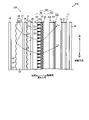
図1は第1の形態を説明する図であり、光学シート30を含む映像源ユニット10の分解斜視図である。また、図2には、図1にII-IIで示した線(鉛直方向に沿った線)に沿って切断した映像源ユニット10の分解断面図の一部、図3にはIII-IIIで示した線(水平方向に沿った線)に沿って切断した映像源ユニット10の分解断面図の一部を表した。なお、ここでいう鉛直方向及び水平方向は、光学シート30が表示装置に配置され、この表示装置が使用される姿勢における向きを意味する。
このような映像源ユニット10は、詳細な説明は省略するが、不図示の筐体に、該映像源ユニット10を作動させる電源、及び映像源ユニット10を制御する電子回路等、映像源ユニット10として動作するために必要とされる通常の機器とともに納められて表示装置とされている。本形態は映像源ユニットの一態様として液晶映像源ユニット、表示装置の一態様として液晶表示装置を説明する。以下映像源ユニット10について説明する。FIG. 1 is a diagram for explaining the first embodiment, and is an exploded perspective view of an
The
映像源ユニット10は、液晶パネル15、面光源装置20、及び機能フィルム40を備えている。本形態で光学シート30は、面光源装置20に含まれている。図1~図3には、表示装置が設置された姿勢における向きを併せて表示している。
The
液晶パネル15は、観察者側に配置された上偏光板13と、面光源装置20側に配置された下偏光板14と、上偏光板13と下偏光板14との間に配置された液晶層12と、を有している。上偏光板13、下偏光板14は、入射した光を直交する二つの偏光成分(P波およびS波)に分解し、一方の方向(透過軸に平行な方向)の偏光成分(例えば、P波)を透過させ、当該一方の方向に直交する他方の方向(吸収軸に平行な方向)の偏光成分(例えば、S波)を吸収する機能を有している。
The
液晶層12は、複数の画素が層面に沿った方向に2次元的に縦横に配列されており、一つの画素を形成する領域毎に電界印加できる。そして電界印加された画素の配向が変化する。これにより、面光源装置20側(すなわち入光側)に配置された下偏光板14を透過した透過軸に平行な偏光成分(例えばP波)は、電界印加された画素を通過する際にその偏光方向を90°回転させ、その一方で、電界印加されていない画素を通過する際にその偏光方向を維持する。このため、画素への電界印加の有無によって、下偏光板14を透過した偏光成分(例えばP波)が、出光側に配置された上偏光板13をさらに透過するか、あるいは、上偏光板13で吸収されて遮断されるか、を制御することができる。
The
このようにして液晶パネル15は、面光源装置20からの光の透過または遮断を画素毎に制御して映像を表現する構造を有している。
In this manner, the
液晶パネルにはいくつかの種類があるが、本形態ではその種類は特に限定されることはなく、公知の型の液晶パネルを用いることができる。具体的には例えばTN、STN、VA、MVA、IPS、OCB等が挙げられる。 Although there are several types of liquid crystal panels, the types are not particularly limited in this embodiment, and known types of liquid crystal panels can be used. Specific examples include TN, STN, VA, MVA, IPS, and OCB.
次に面光源装置20について説明する。
面光源装置20は、液晶パネル15を挟んで観察者側とは反対側に配置され、液晶パネル15に対して面状の光を出射する照明装置である。図1~図3よりわかるように、本形態の面光源装置20は、エッジライト型の面光源装置として構成され、導光板21、光源25、光拡散板26、プリズム層27、反射型偏光板28、光学シート30及び反射シート39を有している。Next, the surface
The surface
導光板21は、図1~図3よりわかるように、基部22及び裏面光学要素23を有している。導光板21は透光性を有する材料により形成された全体として板状の部材である。本形態で導光板21の観察者側となる一方の板面側は平滑面とされ、これとは反対側である他方の板面側は裏面とされ、当該裏面に複数の裏面光学要素23が配列されている。
The
基部22、裏面光学要素23をなす材料としては、種々の材料を使用することができる。ただし、表示装置に組み込まれる光学シート用の材料として広く使用され、優れた機械的特性、光学特性、安定性および加工性等を有するとともに安価に入手可能な材料を用いることができる。これには例えば脂環式構造を有する重合体樹脂、メタクリル樹脂、ポリカーボネート樹脂、ポリスチレン樹脂、アクリロニトリル-スチレン共重合体、メタクリル酸メチル-スチレン共重合体、ABS樹脂、ポリエーテルスルホン等の熱可塑性樹脂や、エポキシアクリレートやウレタンアクリレート系の反応性樹脂(電離放射線硬化型樹脂等)等を挙げることができる。
Various materials can be used as materials for forming the
基部22は、その内部を光が導光されるとともに、裏面光学要素23のベースとなる部位で、適切な厚さを有する板状である。
The
裏面光学要素23は、基部22の裏面側に形成される突出した要素であり、本形態では三角柱状である。本形態で裏面光学要素23は、突出した頂部の稜線が水平方向に延びる柱状であり、複数の裏面光学要素23が当該延びる方向に直交する方向(鉛直方向)に配列されている。本形態の裏面光学要素23は断面が三角形であるがこれに限定されることはなく、多角形、半球状、球の一部、レンズ形状等いずれの形状の断面であってもよい。
複数の裏面光学要素23の配列方向は導光方向であることが好ましい。すなわち、光源25から離隔する方向に配列され、光源25が配列される方向、又は1つの長い光源であれば該光源が延びる方向に平行に各裏面光学要素23の稜線が延びている。The back
The arrangement direction of the plurality of back
なお、本件明細書における「三角形形状」とは、厳密な意味での三角形形状のみでなく、製造技術における限界や成型時の誤差等を含む略三角形形状を含む。また同様に、本件明細書において用いる、その他の形状や幾何学的条件を特定する用語、例えば、「平行」、「直交」、「楕円」、「円」等の用語も、厳密な意味に縛られることなく、同様の光学的機能を期待し得る程度の誤差を含めて解釈する。 In addition, the term "triangular shape" in this specification includes not only a triangular shape in a strict sense, but also a substantially triangular shape including limitations in manufacturing technology, errors during molding, and the like. Similarly, terms specifying other shapes and geometrical conditions used in this specification, such as terms such as “parallel”, “perpendicular”, “elliptical”, “circular”, etc., are also bound by strict meanings. are interpreted with a degree of error that can be expected for similar optical functions.
このような構成を有する導光板21は、押し出し成型により、又は、基部22上に裏面光学要素23を賦型することにより製造することができる。なお、押し出し成型で製造された導光板21においては、基部22、及び裏面光学要素23が一体的に形成され得る。また、賦型によって導光板21を製造する場合、裏面光学要素23が、基部22と同一の樹脂材料であっても、異なる材料であってもよい。
The
図1~図3に戻って、光源25について説明する。光源25は、導光板21の基部22が有する側面(端面)のうち、裏面光学要素23が配列される方向の一方側の側面(端面)に配置される。光源の種類は特に限定されるものではないが、線状の冷陰極管等の蛍光灯、点状のLED(発光ダイオード)、又は白熱電球等の種々の態様で構成できる。本形態で光源25は複数のLEDからなり、不図示の制御装置により各LEDの点灯および消灯、並びに/又は、各LEDの点灯時の明るさを個別に独立して調節できるように構成されている。
なお、本形態では上記のように光源25は一方側の側面(端面)に配置される例を示したが、さらにこの側面(端面)とは反対側となる側面(端面)にも光源が配置される形態であってもよい。この場合には裏面光学要素の形状も当該光源の配置に適するように公知の例に倣って形成する。Returning to FIGS. 1 to 3, the
In this embodiment, the
次に光拡散板26について説明する。光拡散板26は、導光板21の出光側に配置され、ここに入射した光を拡散させて出射する機能を有する層である。これにより、導光板21から出射した光の均一性をさらに高め、導光板21に存在する傷を目立たなくすることができる。
光拡散板の具体的態様は、公知の光拡散板を用いることができ、例えば母材の中に光拡散剤を分散させた形態を挙げることができる。
光拡散板26は、本形態のようにプリズム層27の支持板として用いることもできる。また、導光板21の出光面が平滑の場合には、光拡散板26を導光板21に貼り合わせて一体としてもよい。Next, the
As a specific embodiment of the light diffusing plate, a known light diffusing plate can be used, and for example, a form in which a light diffusing agent is dispersed in a base material can be mentioned.
The
プリズム層27は、図1~図3よりわかるように、光拡散板26よりも液晶パネル15側に設けられ、該液晶パネル15側に向けて凸である単位プリズム27aを具備する層である。本形態で単位プリズム27aは、本形態では三角形断面を有して導光板21の導光方向に直交する方向(本形態では水平方向)に延びる形態を有している。そして、複数の単位プリズム27aが導光板21の導光方向(本形態では鉛直方向)に配列されている。これにより光学機能層32で光を制御する方向(本形態では鉛直方向)に光を集光することができ、光学機能層32で光を効率よく全反射させることが可能となるため、光の利用効率を高めることができる。
ただし、このようなプリズム層の単位プリズムの断面形状は、必要とする機能に応じて公知の形状(三角形、四角形、その他の多角形)を適用することができる。当該形状により上記のように集光することもできるし、逆に光をさらに拡散させることもできる。
また、単位プリズムが延びる方向及び配列される方向は上記形態に限定されることなく他の形態であってもよい。例えば単位プリズムが導光板の導光方向に延び、複数の単位プリズムが導光板の導光方向に対して直交する方向に配列される形態であってもよい。As can be seen from FIGS. 1 to 3, the
However, for the cross-sectional shape of the unit prisms of such a prism layer, a known shape (triangle, quadrangle, other polygon) can be applied according to the required function. Depending on the shape, the light can be focused as described above, or conversely, the light can be further diffused.
Further, the direction in which the unit prisms extend and the direction in which the unit prisms are arranged are not limited to the above-described forms, and other forms may be used. For example, a unit prism may extend in the light guide direction of the light guide plate, and a plurality of unit prisms may be arranged in a direction orthogonal to the light guide direction of the light guide plate.
反射型偏光板28は、入射した光を直交する二つの偏光成分(P波およびS波)に分解し、一方の方向(透過軸に平行な方向)の偏光成分(例えば、P波)を透過させ、当該一方の方向に直交する他方の方向(反射軸に平行な方向)の偏光成分(例えば、S波)を反射する機能を有している。このような反射型偏光板の構造は公知のものを適用することができる。
The reflective
次に光学シート30について説明する。図4には図2の視点で光学シート30の一部を拡大して表した。図1~図4よりわかるように、光学シート30は、シート状に形成された基材層31と、基材層31の一方の面(本形態では導光板21側の面)に設けられた光学機能層32と、基材層31の他方の面(本形態では液晶パネル15側の面)に配置された光制御層としての出光側光制御層35と、を備えている。
Next, the
基材層31は光学機能層32、及び出光側光制御層35を支持する平板状のシート状部材である。
基材層31をなす材料としては、種々の材料を使用することができる。ただし、表示装置に組み込まれる光学シート用の材料として広く使用され、優れた機械的特性、光学特性、安定性および加工性等を有するとともに安価に入手可能な材料を用いることができる。これには例えばポリエチレンテレフタレート樹脂(PET)、トリアセチルセルロース樹脂(TAC)、メタクリル樹脂、ポリカーボネート樹脂等を挙げることができる。この中でも面光源装置20と下偏光板14との組み合わせを考慮して複屈折(リタデーション)の少ないTAC、メタクリル樹脂、ポリカーボネート樹脂を用いることが好ましい。さらには、車載用途などのように高い耐熱性が求められる用途では、ガラス転移点が高いポリカーボネート樹脂が望ましい。具体的にはポリカーボネート樹脂のガラス転移点は143℃であり、一般に105℃での耐久性が求められる車載用途に適している。The
Various materials can be used as the material forming the
光学機能層32は基材層31の一方の面(本形態では導光板21側の面)に積層された層で、光透過部33、及び光吸収部34を有して構成されている。光学機能層32は、図4に示した断面を有して紙面奥/手前側(本形態では映像源ユニット10を正面視したときの水平方向)に延びる形状を備え、層面に沿って当該延びる方向とは異なる方向(本形態では鉛直方向)に光透過部33と光吸収部34とが交互に配列されている。
The
光透過部33は、光を透過させることを主要の機能とする部位であり、本形態では図2、図4に表れる断面において、基材層31側に長い下底、その反対側(導光板21側)に短い上底を有する略台形の断面形状を有する要素である。
光透過部33は、基材層31の層面に沿って当該断面を維持して一方向(本形態では水平方向)に延びるとともに、この延びる方向とは異なる方向(本形態では鉛直方向)に間隔を有して複数配列される。そして、隣り合う光透過部33の間には、略台形断面を有する間隔(溝)が形成されている。従って、当該間隔(溝)は、光透過部33の上底側(導光板21側)に長い下底を有し、光透過部33の下底側(基材層31側)に短い上底を有する台形断面を有し、ここに後述する必要な材料が充填されることにより光吸収部34が形成される。
本形態では、複数の光透過部33がその下底側(基材層側31)でシート状の土台部32aにより連結されている。The
The
In this embodiment, a plurality of light-transmitting
光透過部33は屈折率がNtとされている。このような光透過部33は、光透過部構成組成物を硬化させることにより形成することができる。屈折率Ntの値は特に限定されることはないが、後述するように台形断面の斜面における光吸収部34との界面で適切に光を反射(全反射を含む。)する観点から屈折率は1.47以上であることが好ましい。ただし、屈折率が高すぎる材料は割れやすい場合が多いので屈折率は1.61以下であることが好ましい。より好ましくは1.49以上1.56以下、さらに好ましくは1.56である。The
光吸収部34は隣り合う光透過部33の間に形成された上記の間隔(溝)に形成される間部として機能し、間隔(溝)の断面形状と同様の断面形状となる。従って短い上底が液晶パネル15側(基材層31側)を向き、長い下底がその反対側(本形態では導光板21側)となる。そして光吸収部34は、屈折率がNrとされるとともに、光を吸収することができるように構成されている。具体的には屈折率がNrである透明樹脂に光吸収粒子が分散される。屈折率Nrは、光透過部33の屈折率Ntよりも低い屈折率とされる。このように、光吸収部34の屈折率を光透過部33の屈折率より小さくすることにより、条件を満たして光透過部33に入射した光を光吸収部34との界面で適切に全反射させることができる。また、全反射条件を満たさない場合にも一部の光は当該界面で反射する。
屈折率Nrの値は特に限定されることはなく、当該全反射を適切に行えることを前提に1.47以上であることが好ましい。ただし、屈折率が高すぎる材料は割れやすい場合が多いので屈折率は1.61以下であることが好ましい。より好ましくは1.49以上1.56以下、さらに好ましくは1.49である。The
The value of the refractive index Nr is not particularly limited, and is preferably 1.47 or more on the premise that the total reflection can be properly performed. However, it is preferable that the refractive index is 1.61 or less because a material having an excessively high refractive index tends to crack easily. More preferably 1.49 or more and 1.56 or less, still more preferably 1.49.
光透過部33の屈折率Ntと光吸収部34の屈折率Nrとの屈折率の差は特に限定されるものではないが、0より大きく0.14以下が好ましく、0.05以上0.14以下であることがより好ましい。屈折率差を大きくすることにより、より多くの光を全反射させることができる。The difference in refractive index between the refractive index Nt of the
光学機能層32は、特に限定されることはないが、例えば次のような形状とすることができる。図5には図4の一部をさらに拡大した図を表した。
Although the
図5に示したθ11は、光透過部33と光吸収部34との界面のうち、光学シート30が図1のような姿勢とされた際に光吸収部34の上側となる界面34aと、光学機能層32の層面の法線と、のなす角である。θ12は、同姿勢で光透過部33及び光吸収部34の界面のうち光吸収部34の下側となる界面34bと、光学機能層32の層面の法線と、のなす角である。
θ11は、0°以上10°以下であることが好ましい。θ11が0°より大きいとは導光板21側(入光側)から液晶パネル15側(出光側、基材層31側)に向けて下がるように傾斜することを意味する。
θ12は、0°以上10°以下であることが好ましい。θ12が0°より大きいとは導光板21側(入光側)から液晶パネル15側(出光側、基材層31側)に向けて上がるように傾斜することを意味する。θ 11 shown in FIG. 5 corresponds to the
θ 11 is preferably 0° or more and 10° or less. That θ 11 is greater than 0° means that it is inclined downward from the
θ12 is preferably 0° or more and 10° or less. That θ 12 is greater than 0° means that it is inclined upward from the
θ11、及びθ12の角度の大きさの関係は必要に応じて設定することができる。The relationship between the angles θ 11 and θ 12 can be set as necessary.
また、図4にPaで表した光透過部33及び光吸収部34のピッチは20μm以上100μm以下であることが好ましく、30μm以上100μm以下であることがより好ましい。そして図4にDaで示した光吸収部34の厚さは50μm以上150μm以下であることが好ましく、60μm以上150μm以下であることがより好ましい。これらの範囲内とすることにより、光の透過と光の吸収とのバランスをより適切にすることができる。The pitch between the
本形態では光透過部33と光吸収部34との界面が断面において一直線状となる例を示したが、これに限らず折れ線状、凸である曲線状、凹である曲線状等であってもよい。また、複数の光透過部33及び光吸収部34で断面形状が同じであってもよいし、規則性を有して異なる断面形状であってもよい。
In this embodiment, an example in which the interface between the light transmitting
上記では、光透過部33及び光吸収部34が延びる方向が水平である例を説明したが、モアレ発生を抑制する観点から、光透過部33及び光吸収部34が延びる方向は、液晶層12の画素の配列方向に対して、映像源ユニットの正面視で角度を有していることが好ましい(バイアス角α1)。このバイアス角α1の具体的な角度はモアレの発生を防止できれば特に限定されることはないが、1°以上10°以下であることが好ましい。In the above description, an example in which the direction in which the
次に出光側光制御層35について説明する。出光側光制御層35は光制御層として機能し、光学機能層32と組み合わされることで両者が相まって光の向きを制御する。
本形態では出光側光制御層35は光学機能層32から出光した光に対して光の向きを制御して出射する。すなわち、本形態で出光側光制御層35は、光学機能層32で制御された光の向きをさらに制御して、出光される光が所望の出光角度となるようにする。Next, the output-side
In this embodiment, the output-side
そのため、出光側光制御層35は、支持層35a及び光学要素層35bを有して構成されている。
支持層35aは光学要素層35bの支持体として機能する透明なシート状の部材である。支持層35aは上記した基材層31や光透過部33と同様の材料により構成することができる。Therefore, the output-side
The
光学要素層35bは、光学機能層32から出射した光の向きを変更する層であり、支持層35aの面のうち光学機能層32側とは反対側の面に複数の単位光学要素35cが配列されてなる。
単位光学要素35cは、光学機能層32で制御した光に対してさらに方向制御を行う。本形態では図1~図3の姿勢で、視野角度を鉛直方向上方へ効率よくシフトさせるように制御する。図4、図5には単位光学要素35cの断面形状が表れている。The
The unit
本形態で単位光学要素35cは具体的に次のような構造を備えている。
単位光学要素35cは、基材層31を挟んで光学機能層32側とは反対側に突出する三角形断面を有する三角柱状であり、当該断面を有してその稜線が光透過部33及び光吸収部34が延びる方向と同じ(バイアス角α2=0°)又は光学シートの正面視で角度を有して(バイアス角α2≠0°)延びる突条で構成されている。そして複数の単位光学要素35cが、当該延びる方向とは異なる方向に配列されている。In this embodiment, the unit
The unit
単位光学要素35cの稜線が光透過部33及び光吸収部34が延びる方向に対して光学シートの正面視で角度を有して延びるように構成されている場合(バイアス角α2≠0°)には、光学シート30の正面視で、光学機能層32の光透過部33が延びる方向と、単位光学要素35cの稜線が延びる方向とは0°より大きく45°以下のバイアス角α2で相対的に傾斜するように延びていることが好ましい。これにより光透過部33及び光吸収部34による配列構造と、単位光学要素35cの配列構造と、によるモアレの発生を防止することができる。また、この角度α2を45°より大きくすると、単位光学要素35cによる光方向制御の効率が低下してしまう。より好ましい角度α2は1°以上10°以下である。When the ridgeline of the unit
そして各単位光学要素35cは図5からわかるように、主屈折面35dとライズ面35eとを有している。この主屈折面35d及びライズ面35eが三角柱の2つの面を形成し、他の1つの面が支持層35aに重なって該支持層35aに固定されている。
As can be seen from FIG. 5, each unit
本形態では、主屈折面35dは図1~図5の姿勢で、光学機能層32から出光した光をさらに上方に向けるように光の向きを変える屈折面である。これによれば出光の範囲を鉛直方向上方に効率よく移行させることができる。この場合、主屈折面35dは、下方に向かうにつれて光学機能層32に近づくように傾斜している(ここではこの方向を正(+)の方向の傾きとする。)。従って、1つの単位光学要素35cでは主屈折面35dが下、ライズ面35eが上となる。そして主屈折面35dの傾斜は、光学機能層32の法線方向に対して図5に示したθ21の角度を有する。In this embodiment, the main refracting
θ21の具体的角度は45°より大きく90°未満(主屈折面の傾斜角度の絶対値が45°より大きく90°未満)であることが好ましい。これにより、確実に所望の方向における輝度向上(出光角制御)のための光の制御を行うことができる。θ21が45°以下であると主屈折面35dで全反射が起こりやすく、出光されない光が多くなる虞がある。また、θ21が90°以上であると主屈折面として機能をほとんど発揮できない。
より好ましいθ21は80°以上89°以下である。θ21をこの範囲とすることにより、ライズ面35eを小さく抑えることができ、ライズ面35eによる迷光の発生を少なくすることが可能である。A specific angle of θ21 is preferably greater than 45° and less than 90° (the absolute value of the inclination angle of the main refracting surface is greater than 45° and less than 90°). As a result, it is possible to reliably control the light for improving the luminance (light emission angle control) in a desired direction. If θ21 is 45° or less, total reflection is likely to occur at the
θ21 is more preferably 80° or more and 89° or less. By setting θ21 within this range, the
ライズ面35eは、主屈折面35dを形成するために必要とされる面である。
図5にθ22で表したライズ面35eの傾斜角度は、光学機能層32の層面に沿った方向に対して80°以上100°以下であることが好ましい。製造上の観点から80°以上90°以下がより好ましい。また、θ22が80°未満、及び100°より大きくなるとライズ面35eによる迷光が多くなる虞がある。The
It is preferable that the inclination angle of the
単位光学要素35cの頂角は上記θ21及びθ22からおのずと決まるものであるが、45°以上90°未満であることが好ましい。The apex angle of the unit
図4にPoで示した単位光学要素35cのピッチは、モアレピッチを小さくすることで仮にモアレが発生しても見え難くする観点から、小さいほうが好ましく、具体的にはピッチPoが50μm以下であることが好ましい。
また光学機能層32の方が光学要素層35bより製造難易度が高いことから、光学機能層32の光透過部33のピッチPa(図4参照)より、単位光学要素35cのピッチPoの方が小さい方が望ましい。さらに望ましくは、PoはPaの1/2以下である。最も望ましくはPoを、Pa/2、Pa/3、Pa/4など、等倍ピッチにしたときには、光透過部33の端部と単位光学要素35cの端部とができるだけ一致しないことである。言い換えると、PoとPaとの最小公倍数は大きい方が望ましい。
一方、単位光学要素35cが小さくなると、精度が低下することからPoは10μm以上であることが好ましい。The pitch of the unit optical elements 35c indicated by Po in FIG. 4 is preferably small from the viewpoint of making it difficult to see even if moire occurs by reducing the moire pitch. Specifically, the pitch Po is 50 μm or less. Preferably.
In addition, since the
On the other hand, if the unit
より好ましくは光透過部33の配列ピッチをPa(μm)、単位光学要素35cの配列ピッチをPo(μm)としたとき、Pmx(μm)が10000(μm)以下である。これによりモアレの発生をより確実に防止することができる。ここで、Pmxは次のように得ることができる。
PmxはPmに基づいて得ることができ、Pmは次式で表される。
Pm=|(a・Pa・b・Po)/(a・Pa-b・Po)|More preferably, P mx (μm) is 10000 (μm) or less, where P a (μm) is the arrangement pitch of the
Pmx can be obtained based on Pm , where Pm is expressed by the following equation.
P m =|(a·P a ·b·P o )/(a·P a −b·P o )|
ここで、Pa≧Poであり、a、bは1以上10以下の整数である。そしてPa、Poについて等倍(1倍)ピッチから10倍ピッチまでの全ての組み合わせを考慮する。これにより整数倍ピッチを考慮した広い範囲でモアレ発生について評価することができる。
そして、あるPa、Poの組み合わせに対してa、bを変更した全ての組み合わせのPm中で最大のPmがPmxである。Here, P a ≧P o and a and b are integers of 1 or more and 10 or less. For P a and P o , all combinations from the same (1-fold) pitch to the 10-fold pitch are considered. As a result, it is possible to evaluate moire generation in a wide range considering integral multiple pitches.
Then, P mx is the maximum P m among all combinations of P m obtained by changing a and b for a certain combination of P a and P o .
図4にDoで示した単位光学要素35cの支持層35aからの突出高さは、1μm以上10μm以下であることが好ましい。これより小さくなると、加工精度が悪化して筋状の線が視認される不具合が起こることがあり、これより大きいと、光吸収部34と単位光学要素35cとでモアレが生じやすくなる。The projection height of the unit optical element 35c indicated by Do in FIG. 4 from the
上記形態では、複数の単位光学要素35cが隙間なく連続して配置されているが、これに限らず隣り合う単位光学要素35cの間に間隔を設け、この部分は支持層35aの面が露出する態様であってもよい。
In the above embodiment, the plurality of unit
また、本形態では単位光学要素35cの主屈折面35dが図4、図5に表れる断面において直線状であるが必ずしもこれに限らず、断面において凹状や凸状の曲線や折れ線状であってもよい。
また、主屈折面35d及びライズ面35eを粗面としてもよい。これにより光を散乱してモアレの発生を抑制することができる。主屈折面35d及びライズ面35eを粗面とする方法は特に限定されることはないが、単位光学要素に対して直接ブラスト処理をしたり、単位光学要素を成形する型にブラスト処理をしたりすることが挙げられる。
そして、複数の単位光学要素35cが必ずしも全て同じ形状である必要はなく、適宜変更してもよい。In this embodiment, the main
Also, the main refracting
Further, the plurality of unit
また、本形態では出光側光制御層35に支持層35aを設けたが、支持層35aは必ずしも設ける必要はない。例えば図6に変形例の出光側光制御層35’を表したように、光学要素層35bを基材層31に直接形成してもよい。
このとき、基材層31の面のうち光学要素層35bとの界面を形成する面を粗面とするとともに、基材層31の屈折率と光学要素層35bの屈折率を異なるものとすることができる。これによれば、粗面により光が散乱し、モアレの発生を抑制することが可能である。Further, in this embodiment, the
At this time, the surface of the
このような出光側光制御層35の支持層35a及び光学要素層35b(単位光学要素35c)は、上記した基材層31や光透過部33と同様の材料により構成することができる。
The
光学シート30は例えば次のように作製できる。
はじめに基材層31の一方の面に光透過部33を形成する。これは、光透過部33の形状を転写できる形状を表面に有する金型ロールと、これに対向するように配置されたニップロールとの間に、基材層31となる基材シートを挿入する。このとき、金型ロールとニップロールとの間に間隔を設けることによりこれが土台部32aとなる。そして、基材シートと金型ロールとの間に光透過部を構成する組成物を供給しながら金型ロール及びニップロールを回転させる。これにより金型ロールの表面に形成された光透過部に対応する溝(光透過部形状を反転した形状)に光透過部を構成する組成物が充填され、該組成物が金型ロールの表面形状に沿ったものとなる。The
First, the
ここで、光透過部を構成する組成物としては、例えば、エポキシアクリレート系、ウレタンアクリレート系、ポリエーテルアクリレート系、ポリエステルアクリレート系、ポリチオール系等の電離放射線硬化型の樹脂を挙げることができる。 Here, examples of the composition forming the light transmitting portion include ionizing radiation curable resins such as epoxy acrylate, urethane acrylate, polyether acrylate, polyester acrylate, and polythiol.
金型ロールと基材シートとの間に挟まれ、ここに充填された光透過部を構成する組成物に対し、基材シート側から光照射装置により硬化させるための光を照射する。これにより、組成物を硬化させ、その形状を固定させることができる。そして、離型ロールにより金型ロールから基材層31および成形された光透過部33を離型する。
A light for curing is applied from the side of the base sheet by a light irradiation device to the composition which is sandwiched between the mold roll and the base sheet and which fills the light-transmitting portion. This allows the composition to harden and fix its shape. Then, the release roll releases the
次に光吸収部34を形成する。光吸収部34を形成するには、まず、上記形成した光透過部33間の間隔(溝)に光吸収部を構成する組成物を充填する。その後、余剰分の当該組成物をドクターブレード等で掻き落とす。そして、残った組成物に光透過部33側から紫外線を照射することによって硬化させ、光吸収部34を形成することができる。
Next, the
光吸収部として用いられる材料は特に限定されないが、例えば、ウレタン(メタ)アクリレート、ポリエステル(メタ)アクリレート、エポキシ(メタ)アクリレート、及びブタジエン(メタ)アクリレート等の光硬化型樹脂の中に着色された光吸収粒子が分散されている組成物を挙げることができる。 Although the material used as the light absorbing part is not particularly limited, for example, it is colored in a photocurable resin such as urethane (meth) acrylate, polyester (meth) acrylate, epoxy (meth) acrylate, and butadiene (meth) acrylate. and a composition in which light-absorbing particles are dispersed.
また光吸収粒子を分散させる代わりに顔料や染料により光吸収部全体を着色することもできる。
光吸収粒子を用いる場合には、カーボンブラック等の光吸収性の着色粒子が好ましく用いられるが、これらに限定されるものではなく、映像光の特性に合わせて特定の波長を選択的に吸収する着色粒子を使用してもよい。具体的には、カーボンブラック、グラファイト、黒色酸化鉄等の金属塩、染料、顔料等で着色した有機微粒子や着色したガラスビーズ等を挙げることができる。特に、着色した有機微粒子が、コスト面、品質面、入手の容易さ等の観点から好ましく用いられる。着色粒子の平均粒子径は1.0μm以上20μm以下であることが好ましく、1.0μm以上10μm以下であることがより好ましく、1.0μm以上4.0μm以下であることがさらに好ましい。
ここで「平均粒子径」とは、光吸収粒子を100個電子顕微鏡で観察してその直径を計り、算術平均した直径を意味する。Also, instead of dispersing the light absorbing particles, the entire light absorbing portion can be colored with pigments or dyes.
When light absorbing particles are used, light absorbing colored particles such as carbon black are preferably used, but are not limited to these, and selectively absorb specific wavelengths according to the characteristics of image light. Colored particles may also be used. Specific examples include metal salts such as carbon black, graphite and black iron oxide, organic fine particles colored with dyes and pigments, and colored glass beads. In particular, colored organic fine particles are preferably used from the viewpoints of cost, quality, availability, and the like. The average particle size of the colored particles is preferably 1.0 μm or more and 20 μm or less, more preferably 1.0 μm or more and 10 μm or less, and even more preferably 1.0 μm or more and 4.0 μm or less.
Here, the "average particle size" means the diameter obtained by observing 100 light-absorbing particles with an electron microscope, measuring the diameters, and averaging the diameters.
一方、光学機能層32とは別に支持層35aの一方の面に光学要素層35bを積層した出光側光制御層35を作製しておく。これは光学機能層32において基材層31に光透過部33を積層する方法に倣って、同じ要領で作製することが可能である。ただし、バイアス角α2を0°でない角度とする場合には、光学要素層35bを形成するロール金型のうち単位光学要素35cを成形する溝がロール金型の外周面に沿って螺旋状(ネジ溝状)で形成されたものであることが好ましい。これにより精度の観点及び効率の観点から適切なバイアス角α2を付与することができる。On the other hand, separately from the
そして、基材層31の面のうち光学機能層32が配置された側とは反対側の面と、出光側光制御層35の支持層35aの面のうち、光学要素層35bが配置された側とは反対側の面とを粘着剤により貼り付けて一体化し、光学シート30を得る。
Among the surfaces of the
図1~図3に戻って、面光源装置20の反射シート39について説明する。反射シート39は、導光板21の裏面から出射した光を反射して、再び導光板21内に光を入射させるための部材である。反射シート39は、金属等の高い反射率を有する材料からなるシート、高い反射率を有する材料からなる薄膜(例えば金属薄膜)を表面層として含んだシート等のいわゆる鏡面反射を可能とするものを好ましく適用することができる。
Returning to FIGS. 1 to 3, the
機能フィルム40は、液晶パネル15の出光側に配置され、映像光の質を向上させたり、映像源ユニット10を保護したりする機能を有する層である。これには例えば反射防止フィルム、防眩フィルム、ハードコートフィルム、色調補正フィルム、光拡散フィルム等を挙げることができ、これらが単独又は複数組み合わされて構成されている。
The
次に、以上のような構成を備える映像源ユニット10の作用について、光路例を示しつつ説明する。ただし当該光路例は説明のための概念的なものであり、反射や屈折の程度を厳密に表したものではない。
Next, the operation of the
まず、図2に示すように、光源25から出射した光は、導光板21の側面(端面)である入光面から導光板21内に入射する。図2には、一例として、光源25から導光板21に入射した光L21、L22の光路例が示されている。First, as shown in FIG. 2 , the light emitted from the
図2に示すように、導光板21に入射した光L21、L22は、導光板21の出光側面及びその反対側の裏面において、空気との屈折率差による全反射を繰り返し、導光方向(図2の紙面下方向)へ進んでいく。As shown in FIG. 2, the lights L 21 and L 22 incident on the
ただし、導光板21の裏面には裏面光学要素23が配置されている。このため、図2に示すように、導光板21内を進む光L21、L22は、裏面光学要素23によって進行方向が変わり、全反射臨界角未満の入射角度で出光面、及び裏面に入射することもある。この場合に当該光は、導光板21の出光面及びその反対側の裏面から出射し得る。However, a rear
出光面から出射した光L21、L22は、導光板21の出光側に配置された光拡散板26へと向かう。一方、裏面から出射した光は、導光板21の背面に配置された反射シート39で反射され、再び導光板21内に入射して導光板21内を進むことになる。Lights L 21 and L 22 emitted from the light exit surface travel toward the
導光板21内を進行する光と、裏面光学要素23で向きを変えられて全反射臨界角未満の入射角度で出光面に達する光は、導光板21内の導光方向に沿った各区域において生じる。このため、導光板21内を進んでいる光は、少しずつ、出光面から出射するようになる。これにより、導光板21の出光面から出射する光の導光方向に沿った光量分布を均一化させることができる。
The light traveling through the
導光板21から出射した光は、その後、光拡散板26に達し均一性が高められる。そしてプリズム層27により必要に応じて拡散又は集光されプリズム層27を出光した光は反射型偏光板28に達する。ここでは、反射型偏光板28の透過軸に沿った偏光方向の光は反射型偏光板28を透過し光学シート30に向かう。
一方、反射型偏光板28の反射軸に沿った偏光方向の光は図2に点線矢印で示したように反射して導光板21側に戻される。戻された光は、導光板21、裏面光学要素23、又は反射シート39で反射して再び反射型偏光板28の側に進行する。この反射の際に一部の光の偏光方向が変化しており、その一部は反射型偏光板28を透過する。他の光は再び導光板側に戻される。このように反射型偏光板28で反射した光も反射を繰り返すことで反射型偏光板28を透過できるようになる。これにより光源25からの光の利用率が高められる。
ここで、反射型偏光板28を出射した光は、その偏光方向が下偏光板14の透過軸に沿った方向になっており、下偏光板14を透過する偏光状態の光となっている。The light emitted from the
On the other hand, the light polarized along the reflection axis of the reflective
Here, the light emitted from the reflective
反射型偏光板28を出射した光は光学シート30に達する。光学シート30に入射した光は次のような光路を有して進行する。図7に光学シート30における光路例を表した。
Light emitted from the reflective
光透過部33と光吸収部34とが交互に配列される方向(本形態では鉛直方向)に関して、図2に示した光L21、光L22、及び図7に示した光L71、光L72のように、光透過部33と光吸収部34との界面のうち、光吸収部34の上側となる界面34aに向かう。そして当該界面34aで全反射して、観察者側に向かう斜め上方の光となり、所望の方向への光の制御がなされる。
このとき、光透過部33と光吸収部34との界面のうち光吸収部34の下側である界面34bが、観察者側に向かうにつれて斜め上方となるように傾斜していれば、光L21、光L22、光L71、光L72のような光の進行を光吸収部34が阻害し難くなり、より多くの光を所望の方向に導くことができる。2, and the light L 71 and light L 71 shown in FIG. As indicated by L 72 , among the interfaces between the light transmitting
At this time, if the
また、図7に示したL73は、観察者側に向けて斜め上方に進むとともに、光透過部33と光吸収部34との界面34bで全反射することなく該界面を透過する角度で進行するので、界面34bを透過して光吸収部34に吸収される。
これにより、所望の角度以上の視野角で出射する光を効率よく吸収して遮断することができ、さらに光の進行方向制御を効率よく行うことができる。
また、このような光は液晶パネルに入射して、コントラスト低下や色の反転のような不具合や質の低下を生じる可能性が高いのでこのような光を吸収することができる。In addition, L 73 shown in FIG. 7 travels obliquely upward toward the viewer side, and travels at an angle such that light is transmitted through the
As a result, it is possible to efficiently absorb and block light emitted at a viewing angle greater than or equal to a desired angle, and to efficiently control the traveling direction of light.
In addition, such light can be absorbed because it is highly likely that such light will enter the liquid crystal panel and cause defects such as contrast reduction and color reversal, as well as quality degradation.
光学機能層32を透過した光は、さらに光学要素層35bにて光の向きが変更される。具体的には、本形態では、図7に示した光L71、光L72のように、主屈折面35dで光L71、L72がさらに上方に向けて屈折して出射される。これによりさらに出光範囲を上方に移行(シフト)させることができる。The direction of the light transmitted through the
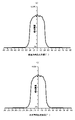
従って、本形態の光学シート30によれば、図8に示したように、出光側光制御層35がない場合(図8のA)に比べて、光学シート30(図8のB)の方がより鉛直方向上方への角度への出光を効率よく高めることができる。図8は、横軸に鉛直方向におけるシート面法線に対する出光角度を表し、正が上方、負が下方である。また縦軸にはある輝度を100%としたときの相対輝度を表した。このような出光角度の調整は光学機能層のみで行うことは難しく、又は行ったとしても輝度の低下等の不具合が伴うことが多い。これに対して光学シート30のように、さらに光学要素層35bを備えることで効率よく出光角度の制御を行うことが可能となる。
そしてこのように光を制御するための光学要素層35bは上記のように簡易な構成であり、このような簡易な構成で効果を有するものとなる。
なお、本形態において光学機能層32の上記θ11、及びθ12(図5参照)をθ11<θ12とすることにより、より広い範囲で視野角の制御をすることができる。Therefore, according to the
The
In this embodiment, by setting θ 11 and θ 12 (see FIG. 5) of the
光学シート30を出射した光は、液晶パネル15の下偏光板14に入射する。下偏光板14は、入射光のうち、一方の偏光成分を透過させ、その他の偏光成分を吸収する。下偏光板14を透過した光は、画素毎への電界印加の状態に応じて、選択的に上偏光板13を透過するようになる。このようにして、液晶パネル15によって、面光源装置20からの光を画素毎に選択的に透過させることにより、液晶表示装置の観察者が、映像を観察することができるようになる。その際、映像光は機能性フィルム40を介して観察者に提供され、映像の質が高められている。
Light emitted from the
図9は第2の形態を説明する図であり、図5に相当する。本形態では出光側光制御層35の代わりに光制御層としての出光側光制御層135が適用されている。他の部位は上記した映像源ユニット10と同じなので、ここでは出光側光制御層135の構成及びその作用について説明する。
FIG. 9 is a diagram for explaining the second embodiment, and corresponds to FIG. In this embodiment, an output-side
出光側光制御層135は光学機能層32から出光した光に対して光の向きを制御して出射する。そのため、出光側光制御層135は、支持層35a及び光学要素層135bを有して構成されている。支持層35aは、上記した出光側光制御層35の支持層35aと同様である。
The output-side
光学要素層135bは、光学機能層32から出射した光の向きを変更する層であり、支持層35aの面のうち光学機能層32側とは反対側の面に複数の単位光学要素135cが配列されてなる。
The
本形態で単位光学要素135cは具体的に次のような構造を備えている。単位光学要素135cは、光学機能層32側とは反対側に突出する三角断面を有する三角柱状であり、当該断面を有してその稜線が光透過部33及び光吸収部34が延びる方向に対して平行(バイアス角α2=0°)、又はバイアス角度(バイアス角α2≠0°)を有して延びる突条で構成されている。そして複数の単位光学要素135cが、当該延びる方向とは異なる方向に配列されている。単位光学要素135cと光透過部33とのバイアス角α2の考え方は上記した単位光学要素35cと同じである。In this embodiment, the unit
そして各単位光学要素135cは図9からわかるように、主屈折面135dとライズ面135eとを有している。この主屈折面135dとライズ面135eが三角柱の2つの面を形成し、他の1つの面が支持層35aに重なって該支持層35aに固定されている。
As can be seen from FIG. 9, each unit
本形態では、主屈折面135dは図1と同様の姿勢で、光学機能層32から上方に向けて出光した光の角度を、正面方向に近づけるように変える屈折面である。これによれば鉛直方向の出光角度を所望の方向に調整できる。この場合、主屈折面135dは、下方に向かうにつれて光学機能層32から離隔する方向に傾斜している(ここではこの方向を負(-)の方向とする。)。従って1つの単位光学要素135cでは主屈折面135dが上、ライズ面135eが下となる。
そして主屈折面135dの傾斜角は、図9に示したように光学機能層32の出光面の法線方向に対してθ31の角度を有している。In this embodiment, the main refracting
The inclination angle of the main refracting
θ31の具体的角度は-89°以上-45°より小さい(傾斜角度の絶対値としては45°より大きく89°以下)であることが好ましい。これにより、確実に所望の方向における輝度向上(出光角制御)のための光の制御を行うことができる。θ31が-45°以上であると主屈折面135dで全反射して出光されない光が多くなる虞がある。また、θ31が-89°より小さくなると主屈折面として機能をほとんど発揮できない。
より好ましいθ31は-89°以上-80°以下(傾斜角度の絶対値としては80°以上89°以下)である。θ31をこの範囲とすることによりライズ面135eが小さくなり、ライズ面135eによる迷光を減らすことができる。A specific angle of θ31 is preferably −89° or more and less than −45° (the absolute value of the inclination angle is more than 45° and less than or equal to 89°). As a result, it is possible to reliably control the light for improving the luminance (light emission angle control) in a desired direction. If θ31 is −45° or more, there is a possibility that a large amount of light is totally reflected by the main
A more preferable θ 31 is −89° or more and −80° or less (80° or more and 89° or less as the absolute value of the tilt angle). By setting θ 31 within this range, the
単位光学要素135cのその他の形状的な観点における好ましい態様は上記した単位光学要素35cと同様に考えることができる。
Other preferable aspects of the unit
次に出光側光制御層135を備えた映像源ユニットの作用について説明する。図10に光路例を示した。なお、他の部位における光路は上記した映像源ユニット10の通りなのでここでは説明を省略する。
Next, the operation of the image source unit provided with the exit-side
光学機能層32を透過した光は、さらに光学要素層135bにて光の向きが変更される。具体的には、本形態では、図10に示した光L101、光L102のように、主屈折面135dで光L101、L102が正面側に近づくように屈折して出射される。これにより出光角度を所望の方向に制御する。The direction of the light transmitted through the
従って、出光側光制御層135を備える光学シートによれば、図11に示したように、出光側光制御層135がない場合(図11のA)に比べて、視野角度を効率よく移行(シフト)させることができる(図11のC)。図11は、横軸に鉛直方向におけるシート面法線に対する出光角度を表し、正が上方、負が下方である。また縦軸にはある輝度を100%としたときの相対輝度を表した。このような出光角度の調整は光学機能層のみで行うことは難しく、又は行ったとしても輝度の低下等の不具合が伴うことが多い。これに対してさらに出光側光制御層135を備えることにより効率よく視野角度の制御を行うことが可能となる。
そしてこのように光を制御するための光学要素層135bは上記のように簡易な構成であり、このような簡易な構成で効果を奏するものとなる。Therefore, according to the optical sheet provided with the output-side
The
図12は第3の形態を説明する図であり、光学シート230を含む映像源ユニット210の分解斜視図である。また、本形態では、上記した光学シート30を光学シート230より入光側(導光板21側)に配置し、光学シート30及び光学シート230の2枚の光学シートで光制御部材229としている。本形態ではわかり易さのため、光学シート30を第一の光学シート30、光学シート230を第二の光学シート230と表記することがある。
FIG. 12 is a diagram for explaining the third embodiment, and is an exploded perspective view of the
図13には、図12にXIII-XIIIで示した線(鉛直方向に沿った線)に沿って切断した映像源ユニット210の分解断面図の一部、図14には図12にXIV-XIVで示した線(水平方向に沿った線)に沿って切断した映像源ユニット210の分解断面図を表した。なお、ここでいう鉛直方向及び水平方向は、光制御部材229が表示装置に配置され、この表示装置が使用される姿勢における向きを意味する。
このような映像源ユニット210も、詳細な説明は省略するが、不図示の筐体に、該映像源ユニット210を作動させる電源、及び映像源ユニット210を制御する電子回路等、映像源ユニット210として動作するために必要とされる通常の機器とともに納められて表示装置とされている。本形態は映像源ユニットの一態様として液晶映像源ユニット、表示装置の一態様として液晶表示装置を説明する。以下映像源ユニット210について説明する。13 shows a part of an exploded cross-sectional view of the
Such
映像源ユニット210は、液晶パネル15、面光源装置220、及び機能フィルム40を備えている。本形態で第一の光学シート230及びこれを含む光制御部材229は、面光源装置20に具備されている。図12~図14には、表示装置が設置された姿勢における向きを併せて表示している。
ここで、液晶パネル15及び機能フィルム40は、上記第1の形態の映像源ユニット10と同様に考えることができるので、ここでは同じ符号を付して説明を省略する。The
Here, since the
面光源装置220は、液晶パネル15を挟んで観察者側とは反対側に配置され、液晶パネル15に対して面状の光を出射する照明装置である。図12~図14よりわかるように、本形態の面光源装置220は、エッジライト型の面光源装置として構成され、導光板21、光源25、光拡散板26、プリズム層27、反射型偏光板28、光制御部材229及び反射シート39を有している。
ここで光制御部材229以外は、上記第1の形態の映像源ユニット10に含まれる面光源装置20と同様に考えることができるので、ここでは同じ符号を付して説明を省略する。The surface
Here, the components other than the
本形態で光制御部材229は、第一の光学シート30及び第二の光学シート230を有して構成されている。これら2枚の光学シートは、第一の光学シート30は導光板21側、第二の光学シート230は液晶パネル15側に配置されている。
ここで第一の光学シート30は、上記面光源装置20に含まれる光学シート30と同様に考えることができるのでここでは同じ符号を付して説明を省略する。In this embodiment, the
Here, the first
図15には図14の視点で第二の光学シート230の一部を拡大して表した。図12~図15よりわかるように、第二の光学シート230は、シート状に形成された基材層231と、基材層231の一方の面(本形態では第一の光学シート30側の面)に設けられた光学機能層232と、基材層231の他方の面(本形態では液晶パネル15側の面)に配置された光制御層としての出光側光制御層235と、を備えている。
ここで基材層231は光学シート30の基材層31と同様に考えることができる。FIG. 15 shows an enlarged view of part of the second
Here, the
光学機能層232は基材層231の一方の面(本形態では第一の光学シート30側の面)に積層された層で、光透過部233、及び光吸収部234を有して構成されている。光学機能層232は、図14、図15に示した断面を有して紙面奥/手前側(本形態では映像源ユニット210を正面視したときの鉛直方向)に延びる形状を備え、層面に沿って当該延びる方向とは異なる方向(本形態では水平方向)に光透過部233と光吸収部234とが交互に配列されている。
The
光透過部233は、光を透過させることを主要の機能とする部位であり、本形態では図14、図15に表れる断面において、基材層231側に長い下底、その反対側(第一の光学シート30側)に短い上底を有する略台形の断面形状を備える要素である。
光透過部233は、基材層231の層面に沿って当該断面を維持して一方向(本形態では鉛直方向)に延びるとともに、この延びる方向とは異なる方向(本形態では水平方向)に間隔を有して複数配列される。そして、隣り合う光透過部34の間には、略台形断面を有する間隔(溝)が形成されている。従って、当該間隔(溝)は、光透過部233の上底側(第一の光学シート30側)に長い下底を有し、光透過部233の下底側(基材層231側)に短い上底を有する台形断面を有し、ここに後述する必要な材料が充填されることにより光吸収部234が形成される。
本形態では、複数の光透過部233がその下底側(基材層231側)でシート状の土台部232aにより連結されている。
このような構成により第一の光学シート30の光透過部33が延びる方向と第二の光学シート230の光透過部233が延びる方向とは光学シートの正面視において交差するように配置されている。The
The light-transmitting
In this embodiment, a plurality of light transmitting
With such a configuration, the direction in which the
光透過部233及び光吸収部234の屈折率については、光学シート30の光透過部33及び光吸収部34と同様に考えることができる。
The refractive indices of the
光学機能層232は、特に限定されることはないが、例えば次のような形状とすることができる。図16には図15の一部(図15の上部)をさらに拡大した図を表した。
Although the
図16に示したθ41は、光透過部233と光吸収部234との界面のうち、第二の光学シート230が図12のような姿勢とされた際に水平方向左右の一方側における界面234aと、光学機能層232の層面の法線と、のなす角である。θ42は、同姿勢で光透過部233と光吸収部234との界面のうち、第二の光学シート230が図12のような姿勢とされた際に水平方向左右の他方側における界面234bと、光学機能層232の層面の法線と、のなす角である。
本形態でθ41、θ42は、0°以上10°以下であることが好ましい。θ41、及びθ42の角度の大きさの関係は必要に応じて設定することができる。θ 41 shown in FIG. 16 is the interface between the
In this embodiment, θ 41 and θ 42 are preferably 0° or more and 10° or less. The relationship between the angles θ 41 and θ 42 can be set as required.
また、図15にPbで表した光透過部233及び光吸収部235のピッチは20μm以上100μm以下であることが好ましく、30μm以上100μm以下であることがより好ましい。そして図15にDbで示した光吸収部234の厚さは50μm以上150μm以下であることが好ましく、60μm以上150μm以下であることがより好ましい。これらの範囲内とすることにより、光の透過と光の吸収とのバランスをより適切にすることができる。Also, the pitch between the light transmitting
本形態では光透過部233と光吸収部234との界面が断面において一直線状となる例を示したが、これに限らず折れ線状、凸である曲線状、凹である曲線状等であってもよい。また、複数の光透過部233及び光吸収部234で断面形状が同じであってもよいし、規則性を有して異なる断面形状であってもよい。
In this embodiment, an example in which the interface between the
上記では、光透過部233及び光吸収部235が延びる方向が鉛直である例を説明したが、モアレ発生を抑制する観点から、光透過部233及び光吸収部234が延びる方向は、液晶層12の画素の配列方向に対して、映像源ユニットの正面視で角度を有していることが好ましい(バイアス角α3)。このバイアス角α3の具体的な角度はモアレの発生を防止できれば特に限定されることはないが、1°以上10°以下であることが好ましい。In the above description, an example in which the
次に出光側光制御層235について説明する。出光側光制御層235は光学機能層232から出光した光に対して光の向きを制御して出射する。本形態で出光側光制御層235は、光学機能層232で制御された光の向きを制御して、出光される光が所望の出光角度となるようにする。より具体的には、シート外周部側から出射される光が、シート法線方向よりも中央側に傾く方向に進行するように光を制御する。
Next, the output-side
そのため、出光側光制御層235は、支持層235a及び光学要素層235bを有して構成されている。
支持層235aは光学要素層235bの支持体として機能する透明なシート状の部材であり、光学シート30の支持層35aと同様に考えることができる。Therefore, the output-side
The
光学要素層235bは、光学機能層232から出射した光の向きを変更する層であり、支持層235aの面のうち光学機能層232側とは反対側の面に複数の単位光学要素235cが配列されてなる。
本形態では、光学要素層235bは支持層235aに配置されているが、これに限らず光学要素層235bが基材層231の面のうち光学機能層232が配置された側とは反対側の面に直接配置されてもよい。この場合には出光側光制御層は支持層を有することなく光学要素層235bのみから構成される。The
In this embodiment, the
本形態で光学要素層235bは、光学機能層232で制御した光に対して複数の単位光学要素235cが配列された方向(本形態では水平方向)において、シート外周側に出射された光が、シート法線方向よりも中央側に傾く方向に出光されるように光の向きを変更する層である。
単位光学要素235cは、図14~図16に表れているように光学機能層232側とは反対側に突出する三角断面を有する三角柱状であり、当該断面を有してその稜線が光透過部233及び光吸収部234が延びる方向と同じ(バイアス角α4=0°)又は光学シートの正面視で角度(バイアス角α4≠0°)を有して延びる(本形態では鉛直方向に延びる)突条で構成されている。そして複数の単位光学要素235cが、当該延びる方向とは異なる方向(本形態では水平方向)に配列されている。
単位光学要素235cの稜線が光透過部233及び光吸収部234が延びる方向に対して光学シートの正面視で角度を有して延びるように構成されている場合(バイアス角α4≠0°)には、光制御部材229の正面視で、光学機能層232の光透過部233が延びる方向と、単位光学要素235cの稜線が延びる方向とは0°<α4≦45°で相対的に傾斜するように延びていることが好ましい。これにより光透過部233及び光吸収部234による配列構造と、単位光学要素235cの配列構造と、によりモアレが発生することを防止することができる。α4を45°より大きくすると、単位光学要素235cによる光の方向制御の効率が低下してしまう。より好ましい角度は1°≦α4≦10°である。In this embodiment, the
As shown in FIGS. 14 to 16, the unit
When the ridgeline of the unit
図15からわかるように、本形態の光学要素層235bは、単位光学要素235cが配列された方向において、単位光学要素235cの断面形状が、光学要素層235bの一端側と他端側とで、シート中央を挟んで対称であるとともに、当該一端側と他端側との間はシート中央部分には単位光学要素235cを有さない部位が具備される(図15のW3の部分)。すなわちこの部分は平坦であり、単位光学要素の主屈折面のシート面法線に対する角度(図16のθ51)が90°である部位であるともいえる。
なお、このような単位光学要素を有しない部位は必ずしも設けられる必要はなく、対称となる単位光学要素235cがシート中央を挟んで隣り合うように構成されてもよい。ただし、このようにシート中央を挟んで隣り合う単位光学要素が対称に存在するとその境界部に線が現れ、これが視認されてしまう虞がある。従って、少なくともシート中央には単位光学要素が存在せず、平坦であることが好ましい。このようにシート中央において線が発生しないようにするために、例えば光学要素層235を形成するための金型を切削加工により作製する際に、このシート中央となるべき部分の金型表面は、この部分を切削工具が跨ぐように重ねて加工すればよい。As can be seen from FIG. 15, in the
It should be noted that it is not always necessary to provide such a portion having no unit optical element, and symmetrical unit
このような複数の単位光学要素235cの配列は、例えばリニアフレネルレンズに倣って構成することもできる。
Such an arrangement of a plurality of unit
単位光学要素235cは図16からわかるように、主屈折面235dとライズ面235eとを有している。この主屈折面235d及びライズ面235eが三角柱の2つの面を形成し、他の1つの面が支持層235aに重なって該支持層235aに固定されている。
As can be seen from FIG. 16, the unit
本形態では、主屈折面235dは、図12~図16の姿勢で、水平方向において、光学機能層232から出光した光を、シート法線に対して中央側に傾いた角度で進行するように向きを変える屈折面である。これによれば単位光学要素235cが配列される方向(本形態では水平方向)において、画面端部から出射された光が中央側に向くので画面中央を正面視する観察者に向けて画面端部の光が向かうことから、観察者が画面端部で出射した光も明るく観察することができる。この場合、1つの主屈折面235dに注目すると、シート中央側に向かうにつれて光学機能層232から遠ざかる方向(より突出する方向)に傾斜している。従って、1つの単位光学要素235cに注目すると主屈折面235dがシート外周側、ライズ面235eがシート中央側となる。そして主屈折面235dの傾斜は、光学機能層232の法線方向に対して図16に示したようにθ51の角度を有している。In this embodiment, the main refracting
θ51の具体的角度は45°より大きく90°未満(主屈折面の傾斜角度の絶対値が45°より大きく90°未満)であることが好ましい。これにより、確実に所望の方向における輝度向上(出光角度制御)のための光の制御を行うことができる。θ51が45°以下であると主屈折面235dで全反射して出光されない光が多くなる虞がある。また、θ51が90°以上であると主屈折面として機能をほとんど発揮できない。より好ましいθ51は80°以上89°以下である。θ51をこの範囲とすることによりライズ面235eが小さくなり、ライズ面235eによる迷光の発生を少なくすることができる。
そしてこのθ51は、単位光学要素235cが配列される方向(本形態では水平方向)において、中央側の単位光学要素235cと外周側の単位光学要素235cとで異なることが好ましい。これによりさらに精度よく光の制御を行うことができる。より好ましくは、中央側の単位光学要素235cから外周側の単位光学要素235cにかけてθ51が小さくなるように構成されている。これにより、中央側への光の進行方向の制御を効率的に行うことができる。A specific angle of θ51 is preferably greater than 45° and less than 90° (the absolute value of the tilt angle of the main refracting surface is greater than 45° and less than 90°). As a result, it is possible to reliably control the light for improving the brightness (light emission angle control) in a desired direction. If θ51 is less than or equal to 45°, there is a possibility that the amount of light that is totally reflected by the
It is preferable that θ 51 is different between the unit
ライズ面235eは、主屈折面235dを形成するために必要とされる面である。
図16にθ52で表したライズ面235eの傾斜角度は、光学機能層232の出光面に沿った方向に対して80°以上100°以下であることが好ましい。製造上の観点から80°以上90°以下がより好ましい。また、θ52が80°未満、及び100°より大きくなるとライズ面235eによる迷光が多くなる虞がある。The
It is preferable that the inclination angle of the rise surface 235e represented by θ52 in FIG. 80° or more and 90° or less is more preferable from the viewpoint of manufacturing. Also, if θ52 is less than 80° or greater than 100°, stray light from the
単位光学要素235cの頂角は上記θ51及びθ52からおのずと決まるものであるが、45°以上90°未満であることが好ましい。The apex angle of the unit
図15にPpで示した単位光学要素235cのピッチは、モアレピッチを小さくすることで仮にモアレが発生しても見え難くする観点から、小さいほうが好ましく、具体的にはピッチPpが50μm以下であることが好ましい。
また光学機能層232の方が光学要素層235bより製造難易度が高いことから、光学機能層232の光透過部233のピッチPb(図15参照)より、単位光学要素235cのピッチPpの方が小さい方が望ましい。さらに望ましくは、PpはPbの1/2以下である。最も望ましくはPpを、Pb/2、Pb/3、Pb/4など、等倍ピッチにしたときには、光透過部233の端部と単位光学要素235cの端部とができるだけ一致しないことである。言い換えると、PpとPbとの最小公倍数は大きい方が望ましい。
一方、単位光学要素235cが小さくなると、精度が低下することからPpは10μm以上であることが好ましい。The pitch of the unit
In addition, since the
On the other hand, if the unit
より好ましくは光透過部233の配列ピッチをPb(μm)、単位光学要素235cの配列ピッチをPp(μm)としたとき、Pmx(μm)が10000(μm)以下である。Pmxは上記と同様に考えることができる。More preferably, P mx (μm) is 10000 (μm) or less, where P b (μm) is the arrangement pitch of the
図15にDpで示した単位光学要素235cの支持層235aからの突出高さは、1μm以上10μm以下であることが好ましい。これより小さくなると、加工精度が悪化して筋状の線が視認される不具合が起こることがあり、これより大きいと、光吸収部234と単位光学要素235cとでモアレが生じやすくなる。The protrusion height of the unit optical element 235c indicated by Dp in FIG. 15 from the
上記形態では、複数の単位光学要素235cが隙間なく連続して配置されているが、これに限らず隣り合う単位光学要素235cの間に間隔を設け、この部分は支持層235aの面が露出する態様であってもよい。
In the above embodiment, the plurality of unit
また、本形態では単位光学要素235cの主屈折面235dが図14~図16に表れる断面において直線状であるが必ずしもこれに限らず、凹状や凸状の曲線や折れ線状であってもよい。
また、主屈折面235d及びライズ面235eを粗面としてもよい。これにより光を散乱してモアレの発生を抑制することができる。主屈折面235d及びライズ面235eを粗面とする方法は特に限定されることはないが、単位光学要素に対して直接ブラスト処理をしたり、単位光学要素を成形する型にブラスト処理をしたりすることが挙げられる。
そして、複数の単位光学要素235cが必ずしも全て同じ形状である必要はなく、適宜変更してもよい。Further, in this embodiment, the main
Also, the main
The plurality of unit
また、本形態では出光側光制御層235に支持層235aを設けたが、上記したように支持層235aは必ずしも設ける必要はなく、光学要素層235bを基材層231に直接形成してもよい。このとき、基材層231の面のうち光学要素層235bとの界面を形成する面を粗面とするとともに、基材層231の屈折率と光学要素層235bの屈折率を異なるものとすることができる。これによれば、粗面により光が散乱し、モアレの発生を抑制することが可能である。
また、出光側光制御層は、必ずしも基材層や光学機能層に一体である必要はなく、別体で設けられてもよい。従って出光側光制御層と、基材層又は光学機能層と、の間に空気層が形成されてもよいし、別の機能層が配置されてもよい。Further, in this embodiment, the
Also, the exit-side light control layer does not necessarily have to be integrated with the base material layer and the optical function layer, and may be provided separately. Therefore, an air layer may be formed between the exit-side light control layer and the substrate layer or the optical functional layer, or another functional layer may be arranged.
このような出光側光制御層235の支持層235a及び光学要素層235b(単位光学要素235c)は、上記した光学シート30の支持層35a及び光学要素層35bと同様の材料により構成することができる。
The
また、第二の光学シート230も光学シート30に倣って上記したように製造することができる。
Also, the second
次に、以上のような構成を備える映像源ユニット210の作用について、光路例を示しつつ説明する。ただし当該光路例は説明のための概念的なものであり、反射や屈折の程度を厳密に表したものではない。また、光源25から出射して光制御部材229に達するまでについては、上記映像源ユニット10で説明した光路例と同様なので説明を省略する(図2参照)。
Next, the operation of the
光制御部材229に入射した光は初めに第一の光学シート30に入射し、次のような光路を有して進行する。図17に第一の光学シート30における光路例を表した。
The light that has entered the
光透過部33と光吸収部34とが交互に配列される方向(本形態では鉛直方向)に関して、図17に示した光L171、光L172のように、光透過部33と光吸収部34との界面のうち、光吸収部34の上側となる界面34aに向かう。そして当該界面34aで全反射して、観察者側斜め上方の光となり、所望の方向への光の制御がなされる。
このとき、光透過部33と光吸収部34との界面のうち光吸収部34の下側である界面34bが、観察者側へ斜め上方に向かうように傾斜していれば、光L171、光L172のような光の進行を光吸収部34が阻害し難くなり、より多くの光を所望の方向に導くことができる。With respect to the direction in which the
At this time, if the
また、図17に示した光L173は、観察者側斜め上方であるとともに、光透過部33と光吸収部34との界面34bで全反射することなく該界面を透過する角度で進行するので、界面34bを透過して光吸収部34に吸収される。
これにより、所望の角度以上の出光角で出射する光を効率よく吸収して遮断することができ、さらに光の進行方向制御を効率よく行うことができる。
また、このような光は液晶パネルに入射して、コントラスト低下や色の反転のような不具合や映像の質の低下を生じる可能性が高いのでこのような光を吸収することができる。Further, the light L 173 shown in FIG. 17 is obliquely upward on the viewer side and travels at an angle that allows it to pass through the
As a result, it is possible to efficiently absorb and block the light emitted at an emission angle equal to or larger than a desired angle, and to efficiently control the traveling direction of the light.
In addition, such light can be absorbed because it is highly likely that such light will enter the liquid crystal panel and cause problems such as contrast reduction and color reversal, as well as image quality degradation.
光学機能層32を透過した光は、さらに光学要素層35bにて光の向きが変更される。具体的には、本形態では、図17に示した光L171、光L172のように、主屈折面35dで光L171、L172がさらに上方に向けて屈折して出射される。これによりさらに出光角度を上方に移行(シフト)させることができる。The direction of the light transmitted through the
従って、本形態の第一の光学シート30でも、図8に示したように、出光側光制御層35がない場合(図8のA)に比べて、第一の光学シート30(図8のB)の方がより鉛直方向上方への出光角度への出光を効率よく高めることができる。このような出光角度の調整は光学機能層32のみで行うことは難しく、又は行ったとしても輝度の低下等の不具合が伴うことが多い。これに対して第一の光学シート30のように、さらに光学要素層35bを備えることで効率よく出光角度の制御を行うことが可能となる。
そしてこのように光を制御するための光学要素層35bは上記のように簡易な構成であり、このような簡易な構成で効果を奏するものとなる。Therefore, even in the first
The
第一の光学シート30を出射した光は第二の光学シート230に達する。第二の光学シート230に入射した光は次のような光路を有して進行する。図15に第二の光学シート230における光路例を表した。
Light emitted from the first
光透過部233と光吸収部234とが交互に配列される方向(本形態では水平方向)に関して、図15に示した光L151~光L156は光透過部233と光吸収部234との界面で全反射して光の向きがシート面法線に近づくように変えられる。これにより光学要素層235bでの所望した光の制御がしやすくなる。With respect to the direction in which the
光L157は、もともと水平方向において正面方向に近い方向に進む光であり、光吸収部234に到達することなく光透過部233を透過する。The light L 157 is originally light traveling in a direction close to the front direction in the horizontal direction, and passes through the
また、図15に示した光L158は、水平方向において正面に対して大きな角度で進行する光である。この光は、光透過部233と光吸収部234との界面で全反射することなく該界面を透過する角度で進行するので、界面を透過して光吸収部234に吸収される。
これにより、所望の角度以上で出射する光を効率よく吸収して遮断することができ、さらに光の進行方向制御を効率よく行うことができる。
また、このような光は液晶パネルに入射して、コントラスト低下や色の反転のような不具合を生じる可能性が高いのでこのような光を吸収することができる。Light L 158 shown in FIG. 15 is light traveling at a large angle with respect to the front in the horizontal direction. Since this light travels at an angle that allows it to pass through the interface between the
As a result, it is possible to efficiently absorb and block light emitted at a desired angle or more, and it is possible to efficiently control the traveling direction of the light.
In addition, since such light is likely to enter the liquid crystal panel and cause problems such as contrast reduction and color reversal, such light can be absorbed.
光学機能層232を透過した光は、さらに光学要素層235bにて光の向きが変更される。具体的には、本形態では、図15に示した光L151、光L152、光L153、光L154のように、主屈折面235dで単位光学要素235cが配列される方向(本形態では水平方向)において、シート面法線に対して中央側に傾斜して光が進行するように光を出射することができる。
なお光L155、L156、L157は単位光学要素235cを備えていない部分を透過するので、水平方向において正面に近い光が出射されそのまま正面の観察者へと光が提供される。The direction of the light transmitted through the
Since the lights L 155 , L 156 , and L 157 pass through the portion not provided with the unit
図18(a)、図18(b)は水平方向におけるシートからの出射光の特徴を説明する図である。図18(a)、図18(b)では、横軸に水平方向におけるシート面法線方向に対する光の出射角度を表し、正が正面に対して右方、負が左方である。縦軸はある輝度を100%としたときの相対輝度である。
図18(a)は出光側光制御層235が設けられていない一つの例を表す。この場合には、光学機能層で出光角度が規制された状態のまま出光されるため、シート面法線に対して小さい傾斜を有する方向にしか(図18(a)の例では概ね-30°以上+30°以下の範囲の方向にしか)出光されない。従って、画面が広い場合や画面を少し斜めから見た場合に、特に画面の外周端部等に暗くなる部位が生じることがあった。
これに対して図18(b)は本形態のように出光側光制御層235を具備した例である。出光側光制御層235のシート外周端部に配置された単位光学要素235cにより図18(b)にC1、C2で示したように、シート外周端部の一方側の単位光学要素235c(C1)及び他方側の単位光学要素235c(C2)のそれぞれから出射された光の出射方向のピークをシート面法線方向(0°方向)にシフトするように制御することができる。また、両外周端部の単位光学要素235cの間に形成された、単位光学要素235cが配置されていないシート中央部分ではDで示したように、そのまま光がシート面法線方向に近い方向で出光される。これにより、画面端部から出射された光も、観察者が見ている方向に向かうように傾斜しているため、画面が広い場合や画面を少し斜めから見た場合にも、画面の外周端部等に暗くなる部位が生じることを防止できる。
このような出光方向角度の調整は光学機能層232のみで行うことは難しく、又は行ったとしても輝度の低下や構造の複雑化を要する等の不具合が伴うことが多い。これに対して第二の光学シート230のように、光学要素層235bを備えることで効率よく出光角度の制御を行うことが可能となる。
そしてこのように光を制御するための光学要素層235bは上記のように簡易な構成であり、このような簡易な構成で効果を奏するものとなる。18(a) and 18(b) are diagrams for explaining the characteristics of light emitted from the sheet in the horizontal direction. In FIGS. 18A and 18B, the horizontal axis represents the light emission angle with respect to the direction normal to the sheet surface in the horizontal direction, with positive being the right side and negative being the left side with respect to the front. The vertical axis is the relative luminance when a certain luminance is taken as 100%.
FIG. 18(a) shows an example in which the exit-side
On the other hand, FIG. 18(b) shows an example in which the output side
Such adjustment of the light output direction angle is difficult to perform only with the
The
このような光制御部材229を光が透過することにより、鉛直方向には所望の方向へ光を出射しつつ、水平方向には外周端部から出射された光を制御することが可能となる。そしてこのような制御を簡易な構成で効率よく行うことができる。
By transmitting light through the
光制御部材229を出射した光は、液晶パネル15の下偏光板14に入射する。下偏光板14は、入射光のうち、一方の偏光成分を透過させ、その他の偏光成分を吸収する。下偏光板14を透過した光は、画素毎への電界印加の状態に応じて、選択的に上偏光板13を透過するようになる。このようにして、液晶パネル15によって、面光源装置220からの光を画素毎に選択的に透過させることにより、液晶表示装置の観察者が、映像を観察することができるようになる。その際、映像光は機能性フィルム40を介して観察者に提供され、映像の質が高められている。
Light emitted from the
本形態では、第一の光学シート30及び第二の光学シート230を組み合わせて光制御部材229として適用した例を説明したが、必ずしも両者は組み合わされている必要はなく、第一の光学シート30及び第二の光学シート230がそれぞれ単独で適用されてもよい。光制御の態様によってそれぞれの光学シートを使い分けても、組み合わせてもよい。
In this embodiment, an example in which the first
図19は第4の形態を説明する図であり、光学シート330を含む映像源ユニット30の分解斜視図である。また、図20には図19にXX-XXで示した線に沿って切断した映像源ユニット310の分解断面図の一部、図21にはXXI-XXIで示した線に沿って切断した映像源ユニット310の分解断面図の一部を表した。
このような映像源ユニット310も、詳細な説明は省略するが、不図示の筐体に、該映像源ユニット310を作動させる電源、及び映像源ユニット310を制御する電子回路等、映像源ユニット310として動作するために必要とされる通常の機器とともに納められて表示装置とされている。本形態は映像源ユニットの一態様として液晶映像源ユニット、表示装置の一態様として液晶表示装置を説明する。FIG. 19 is a diagram for explaining the fourth embodiment, and is an exploded perspective view of
Such
映像源ユニット310は、液晶パネル15、面光源装置320、及び機能フィルム40を備えている。本形態で光学シート330は、面光源装置320に含まれている。図19~図21には、表示装置が設置された姿勢における向きを併せて表示している。
ここで液晶パネル15、及び機能フィルム40については映像源ユニット10と同じであるため同じ符号を付して説明を省略する。The
Since the
面光源装置320は、液晶パネル15より観察者側とは反対側に配置され、液晶パネル15に対して面状の光を出射する照明装置である。図19~図21よりわかるように、本形態の面光源装置320も、エッジライト型の面光源装置として構成され、導光板21、光源25、光拡散板26、プリズム層27、反射型偏光板28、光学シート330及び反射シート39を有している。
ここで、光学シート330以外については、上記した映像源ユニット10の面光源装置20と同じであるため、光学シート330以外の構成については面光源装置30と同じ符号を付して説明を省略する。ただし、本形態ではプリズム層27の単位プリズム27aが導光板の導光方向に延び、複数の単位プリズム27aが導光板の導光方向に対して直交する方向に配列される形態である。The surface
Here, since the components other than the
図22には図20の視点で光学シート330の一部を拡大して表した図を表した。図19~図22よりわかるように、光学シート330は、シート状に形成された基材層31と、基材層31の一方の面(本形態では導光板21側の面)に設けられた光学機能層332と、光制御層として機能する入光側光制御層335と、を備えている。
ここで基材層31は上記した映像源ユニット10の光学シート30に具備された基材層31と同じであるため同じ符号を付して説明を省略する。FIG. 22 shows an enlarged view of a part of the
Here, the
光学機能層332は基材層31の一方の面(本形態では導光板21側の面)に積層された層で、層面に沿って光透過部333と光吸収部334とが交互に配列されている。
The
光学機能層332は、図22に示した断面を有して紙面奥/手前側(映像源ユニット310を正面視したときの水平方向)に延びる形状を備える。すなわち、図22に表れる断面において、略台形である光透過部333と、隣り合う2つの光透過部333の間に形成された断面が略台形の光吸収部334と、を具備している。
The
光透過部333は光を透過させることを主要の機能とする部位であり、本形態では図20、図22に表れる断面において、基材層31側に長い下底、その反対側(導光板21側、入光側光制御層335側)に短い上底を有する略台形の断面形状を有する要素である。光透過部333は、基材層31の層面に沿って当該断面を維持して上記した方向(本形態では水平方向)に延びるとともに、この延びる方向とは異なる方向(本形態では鉛直方向)に間隔を有して配列される。そして、隣り合う光透過部333の間には、略台形断面を有する間隔(溝)が形成されている。従って、当該間隔(溝)は、光透過部333の上底側(導光板21側、入光側光制御層335側)に長い下底を有し、光透過部333の下底側(液晶パネル15側、基材層31側)に短い上底を有する台形断面を有し、ここに後述する必要な材料が充填されることにより光吸収部334が形成される。なお、本形態では隣り合う光透過部333は長い下底側でシート状の連結部332aで連結されている。
The
光透過部333、光吸収部334を構成する材料や屈折率に関する考え方は上記した光学シート30の光透過部33及び光吸収部334と同じである。
The material and refractive index of the
図23には、光透過部333と光吸収部334との界面が光学機能層332の層面の法線に対して成す角θ61、θ62を説明する図を示した。図23は図22の一部をさらに拡大したものである。
θ61は、光透過部333と光吸収部334との界面のうち、光学シート330が図19のような姿勢とされた際に光吸収部334の上側となる界面334aと、光学機能層332の層面の法線と、のなす角である。θ62は、同姿勢で光透過部333及び光吸収部334の界面のうち光吸収部334の下側となる界面334bと、光学機能層332の層面の法線と、のなす角である。FIG. 23 illustrates the angles θ 61 and θ 62 formed by the interface between the
θ 61 is an interface between the
本形態でθ61は、0°以上10°以下であることが好ましい。θ61が0°より大きいとは導光板21側(入光側、入光側光制御層335)から液晶パネル15側(出光側、基材層31側)に向けて下がるように傾斜することを意味する。より好ましくは4.0°以下であり、さらに好ましくは1.0°以下、特に好ましいのは0°である。
θ61を0°より小さくすると製造が困難となる。θ61を10°より大きくすると入光側光制御層335との組み合わせで、光学機能層332による光の向きの制御の効果が小さくなる。また、θ61を10°よりも大きくすると、光吸収部334の配列方向の大きさ(光吸収部の幅、図23の紙面上下方向大きさ)が大きくなり、光の透過率が低下する不具合が生じる傾向にある。In this embodiment, θ61 is preferably 0° or more and 10° or less. θ61 is greater than 0° means that it is inclined downward from the
Making θ61 smaller than 0° makes manufacturing difficult. If θ 61 is larger than 10°, the effect of controlling the direction of light by the
θ62は、0°以上10°以下であることが好ましい。θ62が0°より大きいとは導光板21側(入光側、入光側光制御層335)から液晶パネル15側(出光側、基材層31側)に向けて上がるように傾斜することを意味する。より好ましくは5.0°以下であり、さらに好ましくは3.0°以下である。これにより、光の透過率低下を防止しつつも、上方に向かう光を多くすることができる。θ62を10°よりも大きくすると、光吸収部334の配列方向における大きさ(光吸収部の幅、図23の紙面上下方向大きさ)が大きくなり、光の透過率が低下する不具合が生じる傾向にあり、上方へ向かう光の低減を招くことがある。 θ62 is preferably 0° or more and 10° or less. θ62 is greater than 0° means that it is inclined upward from the
θ61、及びθ62の角度の大きさの関係は、θ61<θ62であることが好ましい。これにより、映像源ユニット310から提供される映像光の視野角に関し、上側の視野角を下側の視野角よりも広くすることができる。The relationship between the angles θ 61 and θ 62 is preferably θ 61 <θ 62 . As a result, regarding the viewing angle of the image light provided from the
また、光学機能層332では、特に限定されることはないが、例えば次のように光透過部333及び光吸収部334が形成される。すなわち、図22にPcで表した光透過部333及び光吸収部334のピッチは20μm以上100μm以下であることが好ましく、30μm以上100μm以下であることがよりに好ましい。そして図22にDcで示した光吸収部334の厚さは50μm以上150μm以下であることが好ましく、60μm以上150μm以下であることがより好ましい。これらの範囲内とすることにより、光の透過と光の吸収とのバランスをより適切にすることができる。Further, in the
本形態では光透過部333と光吸収部334との界面が断面において一直線状となる例を示したが、これに限らず当該界面が折れ線状、凸である曲面状、凹である曲面状等であってもよい。また、複数の光透過部333及び光吸収部334で断面形状が同じであってもよいし、規則性を有して異なる断面形状であってもよい。
In this embodiment, an example in which the interface between the
次に入光側光制御層335について説明する。入光側光制御層35は光制御層として機能し、光学機能層332に入光する光の向きを予め変更し、入光側光制御層335と光学機能層332とで所望の方向への光の出射を制御する。
本形態で入光側光制御層335は、光学シート330の法線方向に進行する光を所望の方向に向かうように光の向きを変えるように構成されている。より具体的に本形態では図19~図22の姿勢で、光学シート330の法線方向観察者側に進行する光に対して観察者側斜め下方に向かうように光の向きを変えるように機能する。これにより後述するように光透過部333と光吸収部334との上側界面334aで反射させ、斜め上方に向かう光にすることができる。Next, the incident-side
In this embodiment, the incident-side
そのため、入光側光制御層335は、支持層335a及び光学要素層335bを有して構成されている。
支持層335aは光学要素層335bの支持体として機能する透明なシート状の部材である。支持層335aは基材層31や光透過部333と同様の材料により構成することができる。Therefore, the incident-side
The
光学要素層335bは、光学機能層332に入光する光の向きを変更する層であり、支持層335aの面のうち光学機能層332が配置される側の面とは反対側の面に複数の単位光学要素335cが配列されてなる層である。単位光学要素335cは、上記のように光学シート330の法線方向に進行する光を一方向に向かうように光の向きを変えるように構成されており、本形態では図19~図22の姿勢で、光学シート330の法線方向に進行する光に対して斜め下方に向かうように光の向きを変えるように構成されている。
The
本形態で単位光学要素335cは具体的に次のような構造を備えている。
単位光学要素335cは、光学機能層332を挟んで基材層31側とは反対側に突出する三角形断面を有する三角柱状であり、当該断面を有してその稜線が光透過部333及び光吸収部334が延びる方向と同じ(バイアス角α5=0°)又は光学シートの正面視で角度を有して(バイアス角α5≠0°)延びる突条で構成されている。そして複数の単位光学要素335cが、当該延びる方向とは異なる方向に配列されている。In this embodiment, the unit
The unit
単位光学要素335cの稜線が光透過部333及び光吸収部334が延びる方向に対して光学シートの正面視で角度を有して延びるように構成されている場合(バイアス角α5≠0°)には、光学シート330の正面視で、光学機能層332の光透過部333が延びる方向と、単位光学要素335cの稜線が延びる方向とは0°より大きく45°以下のバイアス角α5で相対的に傾斜するように延びていることが好ましい。これにより光透過部333及び光吸収部334による配列構造と、単位光学要素335cの配列構造と、によるモアレの発生を防止することができる。また、この角度α5を45°より大きくすると、単位光学要素335cによる光方向制御の効率が低下してしまう。より好ましい角度α5は1°以上10°以下である。When the ridgeline of the unit
そして、単位光学要素335cは図23からわかるように、主屈折面335dとライズ面335eとを有して構成されている。この主屈折面335d及びライズ面335eが三角柱の2つの面を形成し、他の1つの面が支持層335aに重なって該支持層335aに固定されている。
As can be seen from FIG. 23, the unit
主屈折面335dは図19~図23の姿勢で、光学シート330の法線方向に進行する光に対して斜め下方に向かうように光の向きを変えるように機能する屈折面である。従って、主屈折面335dは鉛直方向上側において支持層335a(光学機能層332)に近く、鉛直方向下側において支持層335a(光学機能層332)から離隔するように傾斜している。そして図23にθ71で表した傾斜は、光学機能層332の入光面332bに沿った方向に対して角度を有している。θ71の具体的角度は0°より大きく17°より小さいことが好ましい。これにより、より確実に所望の方向における輝度向上のための光の制御を行うことができる。19 to 23, the
ライズ面335eは、主屈折面335dを形成するために必要とされる面である。ただし、後で説明するように、当該ライズ面335eから入射する光はここで屈折され、光吸収部334に吸収され易い角度で光学機能層332を進行するので、出射させたくない方向の光をより確実に遮断する機能も有する。
θ72で表したライズ面335eの傾斜は、光学機能層332の入光面332bに沿った方向に対して90°以下であることが好ましい。この角度が90°以上となると製造が難しくなる。一方、θ72は73°以上であることが好ましい。これにより、主屈折面335dとライズ面335eとの成す角を90°又はこれに近い角度とすることができ、主屈折面335dの法線方向から主屈折面335dに入射した光が、ライズ面335eに対して平行に近い方向で進むことができるため、ライズ面335eで反射して迷光となることを抑制することができる。The
The inclination of the
図22にPqで示した単位光学要素335cのピッチは、光吸収部334のピッチPcよりも小さいことが好ましく、Pcに対して2/3、2/5など、整数倍ピッチにならないことがさらに好ましい。これにより、光吸収部334と単位光学要素335cとによるモアレの発生を防止することができる。また、より好ましくは、上記の条件を満たしつつPqが3μm以上である。Pqがこれより小さくなると加工精度が悪化する不具合がある。
また、図22にDqで示した単位光学要素335cの支持層335aからの突出高さは、1μm以上15μm以下であることが好ましい。これより小さくなると、加工精度が悪化する不具合があり、これより大きいと、光吸収部334と単位光学要素335cとでモアレが生じやすくなる。The pitch of the unit
Also, the height of the unit optical element 335c shown by Dq in FIG. If it is smaller than this, there is a problem that the processing accuracy deteriorates.
上記形態では、複数の単位光学要素335cが隙間なく連続して配置されているが、これに限らず隣り合う単位光学要素335cの間に間隔を設け、この部分は支持層335aの面が露出する態様であってもよい。
また、複数の単位光学要素335cが必ずしも同じ形状である必要はなく、適宜変更してもよい。In the above embodiment, the plurality of unit
Also, the plurality of unit
このような入光側光制御層335の支持層335a及び光学要素層335b(単位光学要素335c)は、上記した基材層31や光透過部33と同様の材料により構成することができる。
The
次に、以上のような構成を備える映像源ユニット310の作用について、光路例を示しつつ説明する。ただし当該光路例は説明のための概念的なものであり、反射や屈折の程度を厳密に表したものではない。
Next, the operation of the
まず、図20に示すように、光源25から出射した光は、導光板21の側面(端面)である入光面から導光板21内に入射する。図20には、一例として、光源25から導光板21に入射した光L201、L202の光路例が示されている。First, as shown in FIG. 20 , the light emitted from the
図20に示すように、導光板21に入射した光L201、L202は、導光板21の出光側面及びその反対側の裏面において、空気との屈折率差による全反射を繰り返し、導光方向(図20の紙面下方向)へ進んでいく。As shown in FIG. 20, lights L 201 and L 202 incident on the
ただし、導光板21の裏面には裏面光学要素23が配置されている。このため、図20に示すように、導光板21内を進む光L201、L202は、裏面光学要素23によって進行方向が変わり、全反射臨界角未満の入射角度で出光面、及び裏面に入射することもある。この場合に当該光は、導光板21の出光面及びその反対側の裏面から出射し得る。However, a rear
出光面から出射した光L201、L202は、導光板21の出光側に配置された光拡散板26へと向かう。一方、裏面から出射した光は、導光板21の背面に配置された反射シート39で反射され、再び導光板21内に入射して導光板21内を進むことになる。Lights L 201 and L 202 emitted from the light exit surface travel toward the
導光板21内を進行する光と、裏面光学要素23で向きを変えられて全反射臨界角未満の入射角度で出光面に達する光は、導光板21内の導光方向に沿った各区域において生じる。このため、導光板21内を進んでいる光は、少しずつ、出光面から出射するようになる。これにより、導光板21の出光面から出射する光の導光方向に沿った光量分布を均一化させることができる。
The light traveling through the
導光板21から出射した光は、その後、光拡散板26に達し均一性が高められる。そしてプリズム層27により必要に応じて拡散又は集光されプリズム層27を出光した光は反射型偏光板28に達する。ここでは、反射型偏光板28の透過軸に沿った偏光方向の光は反射型偏光板28を透過し光学シート330に向かう。
一方、反射型偏光板28の反射軸に沿った偏光方向の光は図20に点線矢印で示したように反射して導光板21側に戻される。戻された光は、導光板21、裏面光学要素23、又は反射シート39で反射して再び反射型偏光板28の側に進行する。この反射の際に一部の光の偏光方向が変化しており、その一部は反射型偏光板28を透過する。他の光は再び導光板側に戻される。このように反射型偏光板28で反射した光も反射を繰り返すことで反射型偏光板28を透過できるようになる。これにより光源25からの光の利用率が高められる。
ここで、反射型偏光板28を出射した光は、その偏光方向が下偏光板14の透過軸に沿った方向になっており、下偏光板14を透過する偏光状態の光となっている。The light emitted from the
On the other hand, the light polarized along the reflection axis of the reflective
Here, the light emitted from the reflective
反射型偏光板28を出射した光は光学シート330に達する。光学シート330に入射した光は次のような光路を有して進行する。図24には光学シート330における光路例を表した。
図20に示した光L201、光L202、及び図24に示した光L241、光L242は、単位光学要素335cの主屈折面335dに入射し、当該主屈折面335dへの入射角度に応じて屈折、又は屈折することなく主屈折面335dを透過する(主屈折面335dの傾斜面に直交する方向から入射した光は屈折することなく主屈折面335dを透過する(光L242)。)。これにより多くの光が観察者側斜め下方に向いた光となり、これが光透過部333と光吸収部334との界面のうち、光吸収部334の上側となる界面334aに向かう。そして当該界面334aで全反射して、観察者側斜め上方の光となり、所望の方向への光の制御がなされる。特に界面334aの傾斜角θ61(図23参照)が0°であればより上方へ光を向かわせることができる。一方、θ61を調整することにより上方でありつつも所望の範囲に光を向かわせることも可能である。
このとき、光透過部333と光吸収部334との界面のうち光吸収部334の下側である界面334bが、観察者側斜め上方に向かうように傾斜していれば、光L201、光L202、光L241、光L242のような光の進行を光吸収部334が阻害し難くなり、より多くの光を所望の方向に導くことができる。Light emitted from the reflective
Light L 201 and light L 202 shown in FIG. 20, and light L 241 and light L 242 shown in FIG. (light incident from a direction orthogonal to the inclined surface of the main refracting
At this time, if the
従って、光学シート330では、図23にθ71で表した主屈折面335cの傾斜角と、図23にθ61で表した界面334aの傾斜角との組み合わせにより、光を効率よく所望の方向に導くことを容易に行うことができる。いずれか一方では、導く光の方向に限界があり、組み合わせにより相乗的に作用してより容易に光の進行方向を制御することが可能となる。Therefore, in the
また、図20に示した光L203、図24に示したL243は、単位光学要素335cのライズ面335eに入射し、当該ライズ面335eへの入射角度に応じて屈折又は屈折することなくライズ面335eを透過する。このようにしてライズ面335eを透過した光は、その多くが観察者側斜め上方であるとともに、光透過部333と光吸収部334との界面334bで全反射することなく該界面を透過する角度で進行するので、界面334bを透過して光吸収部334に吸収される。
これにより、所望の角度以上の視野角で出射する光を効率よく吸収して遮断することができ、さらに光の進行方向制御を効率よく行うことができる。
また、このような光は液晶パネルに入射して、コントラスト低下や色の反転のような不具合を生じる可能性が高いのでこのような光を吸収することができる。Light L 203 shown in FIG. 20 and light L 243 shown in FIG. 24 enter the
As a result, it is possible to efficiently absorb and block light emitted at a viewing angle greater than or equal to a desired angle, and to efficiently control the traveling direction of light.
In addition, since such light is likely to enter the liquid crystal panel and cause problems such as contrast reduction and color reversal, such light can be absorbed.
光学シート330を出射した光は、液晶パネル15の下偏光板14に入射する。下偏光板14は、入射光のうち、一方の偏光成分を透過させ、その他の偏光成分を吸収する。下偏光板14を透過した光は、画素毎への電界印加の状態に応じて、選択的に上偏光板13を透過するようになる。このようにして、液晶パネル15によって、面光源装置320からの光を画素毎に選択的に透過させることにより、液晶表示装置の観察者が、映像を観察することができるようになる。その際、映像光は機能性フィルム40を介して観察者に提供され、映像の質が高められている。
Light emitted from the
以上のように、光学シート330によれば、光学要素層335bにおける屈折、及び光透過部333と光吸収部334との界面334aでの全反射により、光学シート330に入射した光を上方向へ出射しやすくなっており、下方向への出射は制限されている。すなわち、例えば光学シート330を用いることにより、入射した光をドライバー視点となる上方向に効率よく出射し、上方向に出射する光の輝度を向上させることができる。一方で、大きく上方に出射する光を光吸収部で吸収し易くしているので、フロントガラスへの写り込みを防止することが可能となる。
従って、本形態の光学シートを液晶表示装置に用いることにより、従来の光学シートを使用した場合に比べ、容易に光を制御して、ドライバー視点での視認性を向上させることができる。As described above, according to the
Therefore, by using the optical sheet of this embodiment in a liquid crystal display device, it is possible to easily control light and improve the visibility from the driver's viewpoint, as compared with the case of using a conventional optical sheet.
これによれば例えば図25に示したような出光特性を容易に実現できる。図25は横軸に鉛直方向の視野角、縦軸に相対輝度を表したグラフである。横軸は正(+)が鉛直方向上方、負(-)が鉛直方向下方を表している。
図25からわかるように、鉛直方向の視野角を見た場合に、図25にDで示した位置からわかるように相対輝度のピークが+20°(鉛直方向上方20°)近傍となっている。すなわち、正面(0°)とは異なる観察者の視点となる方向に輝度ピークがあるように光が制御されている。さらに図25にEで示した位置からわかるように、+50°(鉛直方向上方50°)近傍にて急激に相対輝度が低下している。すなわち、自動車におけるフロントガラスへの映り込みの原因となるような大きく上方に進行する光をより確実に遮断することができる。According to this, for example, the light output characteristics as shown in FIG. 25 can be easily realized. FIG. 25 is a graph in which the horizontal axis represents the viewing angle in the vertical direction and the vertical axis represents the relative brightness. On the horizontal axis, positive (+) indicates vertical upward and negative (-) indicates vertical downward.
As can be seen from FIG. 25, when viewing the viewing angle in the vertical direction, the peak of the relative luminance is near +20° (20° upward in the vertical direction) as can be seen from the position indicated by D in FIG. That is, the light is controlled so that the brightness peak is in the direction of the observer's viewpoint, which is different from the front (0°). Furthermore, as can be seen from the position indicated by E in FIG. 25, the relative luminance sharply drops near +50° (50° upward in the vertical direction). In other words, it is possible to more reliably block light that travels significantly upward and causes reflection on the windshield of an automobile.
以下には、上記した各形態について光学シート、及び映像源ユニットを構成してその性能を試験した。 In the following, optical sheets and image source units were constructed for each of the above-described forms, and their performance was tested.
{試験例A}
実施例Aでは、映像源ユニット10の例に倣って、光学シートの出光方向制御の観点で試験を行った。{Test example A}
In Example A, following the example of the
[試験例Aの光学シートの構成]
<試験例A1>
試験例A1では、出光側光制御層35を備える映像源ユニット10の例に倣って図5に表したθ21を変更した光学シートを作製した。θ21以外の光学シートの具体的な形状は次のとおりである。[Structure of Optical Sheet of Test Example A]
<Test example A 1 >
In Test Example A1, an optical sheet was produced in which θ21 shown in FIG. The specific shape of the optical sheet other than θ21 is as follows.
(基材層)
・材料:ポリカーボネート樹脂
・厚さ:130μm(Base material layer)
・Material: Polycarbonate resin ・Thickness: 130 μm
(光学機能層)
・光透過部、及び光吸収部のピッチ(図4のPa):39μm
・光吸収部上底幅(図4のWa):4μm
・光吸収部下底幅(図4のWb):10μm
・光吸収部上側傾斜角(図5のθ11):3°
・光吸収部下側傾斜角(図5のθ12):0°
・光吸収部の厚さ(図4のDa):102μm
・光学機能層の厚さ:127μm
・土台部の厚さ:25μm
・光透過部の材料及び屈折率:屈折率1.56の紫外線硬化型ウレタンアクリレート樹脂
・光吸収部の材料及び屈折率:屈折率1.49の紫外線硬化型ウレタンアクリレート樹脂にカーボンブラックを含有した平均粒子径4μmのアクリルビーズを20質量%分散
・光透過部及び光吸収部が液晶層の画素配列方向に対する傾斜角(バイアス角α1):5°(Optical function layer)
・Pitch between light transmitting portion and light absorbing portion (P a in FIG. 4): 39 μm
・Light absorbing part upper base width (W a in FIG. 4): 4 μm
・Lower width of light absorbing portion (W b in FIG. 4): 10 μm
・Upper inclination angle of the light absorbing portion (θ 11 in FIG. 5): 3°
・Light absorbing part lower side inclination angle (θ 12 in Fig. 5): 0°
・Thickness of light absorbing portion (D a in FIG. 4): 102 μm
・Thickness of optical function layer: 127 μm
・Thickness of the base part: 25 μm
・Material and refractive index of the light transmitting part: UV curable urethane acrylate resin with a refractive index of 1.56 ・Material and refractive index of the light absorbing part: UV curable urethane acrylate resin with a refractive index of 1.49 containing carbon black Acrylic beads with an average particle diameter of 4 μm are dispersed at 20% by mass ・The angle of inclination (bias angle α 1 ) of the light transmitting portion and the light absorbing portion with respect to the pixel arrangement direction of the liquid crystal layer: 5°
(出光側光制御層)
・ライズ面の角度(図5のθ22):90°
・単位光学要素のピッチ(図4のPo):18μm
・単位光学要素の材料:屈折率1.50の紫外線硬化型ウレタンアクリレート樹脂
・上記バイアス角α1に対する傾斜角(バイアス角α2):3°
ここで、バイアス角α2は、光学シートの正面視でバイアス角α1と同じ方向に回転するような角度である(以下の例も同様である。)。従って本例では単位光学要素が延びる方向が液晶層の画素配列方向に対する傾斜角はα1+α2=8°となる。
・主屈折面の角度(図5のθ21):85°(試験例A1-1)、80°(試験例A1-2)、70°(試験例A1-3)、60°(試験例A1-4)(Outgoing side light control layer)
・The angle of the rise surface (θ 22 in FIG. 5): 90°
・Pitch of unit optical element (P o in FIG. 4): 18 μm
・Material of unit optical element: UV curable urethane acrylate resin with a refractive index of 1.50 ・Inclination angle ( bias angle α2) with respect to the bias angle α1: 3 °
Here, the bias angle α2 is an angle that rotates in the same direction as the bias angle α1 when the optical sheet is viewed from the front ( the same applies to the following examples). Therefore, in this example, the direction in which the unit optical elements extend has an inclination angle of α 1 +α 2 =8° with respect to the pixel arrangement direction of the liquid crystal layer.
・Angle of main refracting surface (θ 21 in FIG. 5): 85° (Test Example A 1-1 ), 80° (Test Example A 1-2 ), 70° (Test Example A 1-3 ), 60° ( Test Example A 1-4 )
<試験例A2>
試験例A2では、図9に示した出光側光制御層135を備える映像源ユニットの例に倣ってθ31を変更した光学シートを作製した。出光側光制御層135以外の構成は試験例A1と同じである。またライズ面の角度も90°で一定とした。そして、主屈折面の角度(図9のθ31)は、85°(試験例A2-1)、80°(試験例A2-2)、70°(試験例A2-3)、60°(試験例A2-4)である。<Test example A 2 >
In Test Example A2 , an optical sheet was produced in which θ 31 was changed following the example of the image source unit provided with the exit-side
<試験例A3>
試験例A3では、試験例A2-2の光学シートに対して、ライズ面の角度(図5のθ22に相当)を80°(試験例A3-1)、及び100°(試験例A3-2)とした。それ以外は試験例A2-2と同じである。<Test Example A 3 >
In Test Example A 3 , with respect to the optical sheet of Test Example A 2 -2, the angle of the rise surface (corresponding to θ 22 in FIG. 5) was set to 80° (Test Example A 3 -1) and 100° (Test Example A 3-2 ). Other than that, it is the same as Test Example A 2 -2.
<試験例A4>
試験例A4は、試験例A1の光学シートから出光側光制御層を除外した構成の光学シートである。他の部位は試験例A1の光学シートと同じとした。<Test Example A 4 >
Test Example A4 is an optical sheet having a configuration in which the exit - side light control layer is removed from the optical sheet of Test Example A1. Other parts were the same as those of the optical sheet of Test Example A1 .
[試験例Aの評価方法]
上記各光学シートをモデル化し、シミュレーションで出光角度と各出光角度における輝度の関係を得た。シミュレーションソフトとして、Light Tools(Synopsys社)を用いた。光源の特性を図26に示した。図26の横軸は鉛直方向における視野角度(正が上方、負が下方)、縦軸には視野角度が0°のときの輝度を100%として相対輝度を表した。[Evaluation method of Test Example A]
Each of the above optical sheets was modeled, and the relationship between the light output angle and the luminance at each light output angle was obtained by simulation. Light Tools (Synopsys) was used as simulation software. FIG. 26 shows the characteristics of the light source. The horizontal axis of FIG. 26 represents the viewing angle in the vertical direction (positive is upward, negative is downward), and the vertical axis represents the relative luminance with the luminance at the viewing angle of 0° being 100%.
[試験例Aの結果]
図27には試験例A1、図28に試験例A2、図29に試験例A3の結果を示した。図27~図29では試験例A4のグラフをA4で表した。
そして図27では試験例A1-1をA1-1、試験例A1-2をA1-2、試験例A1-3をA1-3、試験例A1-4をA1-4で表した。
同様に図28では試験例A2-1をA2-1、試験例A2-2をA2-2、試験例A2-3をA2-3、試験例A2-4をA2-4で表した。
そして図29では試験例A3-1をA3-1、試験例A3-2をA3-2と表記した。また図29には合わせてA2-2も表示してある。
各グラフは、横軸に鉛直方向における視野角度を表し、正が上方、負が下方である。また縦軸には図26に示した光源特性を100%としたときの相対輝度を表した。[Results of Test Example A]
FIG. 27 shows the results of Test Example A 1 , FIG. 28 shows the results of Test Example A 2 , and FIG. 29 shows the results of Test Example A 3 . In FIGS. 27 to 29, the graph of Test Example A4 is indicated by A4.
In FIG. 27, Test Example A 1 -1 is A 1 -1, Test Example A 1 -2 is A 1 -2, Test Example A 1 -3 is A 1 -3, and Test Example A 1 -4 is A 1 -. 4.
Similarly, in FIG. 28, Test Example A 2 -1 is changed to A 2 -1, Test Example A 2 -2 is changed to A 2 -2, Test Example A 2 -3 is changed to A 2 -3, and Test Example A 2 -4 is changed to A 2 -4.
In FIG. 29, Test Example A 3 -1 is indicated as A 3 -1, and Test Example A 3 -2 is indicated as A 3 -2. In addition, A 2 -2 is also displayed in FIG.
In each graph, the horizontal axis represents the viewing angle in the vertical direction, with positive being upward and negative being downward. The vertical axis represents the relative brightness when the light source characteristics shown in FIG. 26 are assumed to be 100%.
これら図からわかるように、試験例A1、A2、A3にかかる光学シートにより、試験例A4にかかる光学シートに比べて出光角度を所望の方向に細かく、効率よく制御することができた。As can be seen from these figures, the optical sheets according to Test Examples A 1 , A 2 , and A 3 can finely and efficiently control the light output angle in a desired direction as compared with the optical sheet according to Test Example A 4 . rice field.
試験例A1-3、試験例A1-4、試験例A2-3、試験例A2-4のように出光角を大きく移行(シフト)するように変更した場合、及び、試験例A3-1、試験例A3-2のようにライズ面の角度を90°より大きく、又は小さくした場合には出光角度が+又は-側の60°~90°の範囲で相対輝度が増えることがある。これらはライズ面における迷光であると考えられる。ただし、このような迷光は偏光板で多くを吸収することができるため、不具合とは成り難い。Test Example A 1-3 , Test Example A 1-4 , Test Example A 2-3 , and Test Example A 2-4 in which the light output angle is changed to greatly shift (shift), and Test Example A 3-1 , Test Example A When the angle of the rise surface is made larger or smaller than 90° as in 3-2 , the relative brightness increases in the range of 60° to 90° on the + or - side of the light output angle. There is These are considered to be stray lights on the rise surface. However, since a large amount of such stray light can be absorbed by the polarizing plate, it is unlikely to become a problem.
{試験例B}
試験例Bでは、映像源ユニット210の例に倣って、光学シートの出光方向制御の観点で試験した。{Test example B}
In Test Example B, following the example of the
[試験例B1の光制御部材の構成]
試験例B1では、光制御部材229の例に倣って光制御部材を作製した。具体的な態様は次の通りである。[Configuration of Light Control Member of Test Example B 1 ]
In Test Example B1 , a light control member was produced following the example of the
<第一の光学シート>
(基材層)
・材料:ポリカーボネート樹脂
・厚さ:130μm<First optical sheet>
(Base material layer)
・Material: Polycarbonate resin ・Thickness: 130 μm
(光学機能層)
・光透過部、及び光吸収部のピッチ(図4のPa):47μm
・光吸収部上底幅(図4のWa):3μm
・光吸収部下底幅(図4のWb):22μm
・光吸収部上側傾斜角(図5のθ11):4.5°
・光吸収部下側傾斜角(図5のθ12):4.5°
・光吸収部の厚さ(図4のDa):120μm
・光学機能層の厚さ:145μm
・土台部の厚さ:25μm
・光透過部の材料及び屈折率:屈折率1.56の紫外線硬化型ウレタンアクリレート樹脂
・光吸収部の材料及び屈折率:屈折率1.49の紫外線硬化型ウレタンアクリレート樹脂にカーボンブラックを含有した平均粒子径4μmのアクリルビーズを20質量%分散(Optical function layer)
・Pitch between light transmitting portion and light absorbing portion (P a in FIG. 4): 47 μm
・Light absorbing portion upper bottom width (W a in FIG. 4): 3 μm
・Bottom width of light absorbing portion (W b in FIG. 4): 22 μm
・Upper tilt angle of light absorbing portion (θ 11 in FIG. 5): 4.5°
・Light absorbing part lower side inclination angle (θ 12 in Fig. 5): 4.5°
・Thickness of light absorbing portion (D a in FIG. 4): 120 μm
・Thickness of optical function layer: 145 μm
・Thickness of the base part: 25 μm
・Material and refractive index of the light transmitting part: UV curable urethane acrylate resin with a refractive index of 1.56 ・Material and refractive index of the light absorbing part: UV curable urethane acrylate resin with a refractive index of 1.49 containing
(出光側光制御層)
・主屈折面の傾斜角度(図5のθ21):70°
・ライズ面の傾斜角度(図5のθ22):90°
・支持層の厚さ:25μm
・単位光学要素のピッチ(図4のPo):26μm
・単位光学要素の材料:屈折率1.50の紫外線硬化型ウレタンアクリレート樹脂
・光透過部が延びる方向に対する単位光学要素が延びる方向のバイアス角α3:5°(Outgoing side light control layer)
・Inclination angle of the main refracting surface (θ 21 in FIG. 5): 70°
・Inclination angle of rise surface (θ 22 in FIG. 5): 90°
・Thickness of support layer: 25 μm
・Pitch of unit optical element (P o in FIG. 4): 26 μm
・Material of the unit optical element: UV curable urethane acrylate resin with a refractive index of 1.50 ・Bias angle α 3 of the direction in which the unit optical element extends with respect to the direction in which the light transmission part extends: 5°
<第二の光学シート>
(基材層)
・材料:ポリカーボネート樹脂
・厚さ:130μm<Second optical sheet>
(Base material layer)
・Material: Polycarbonate resin ・Thickness: 130 μm
(光学機能層)
・光透過部、及び光吸収部のピッチ(図15のPb):47μm
・光吸収部上底幅(図15のWc):3μm
・光吸収部下底幅(図15のWd):22μm
・光吸収部一方側傾斜角(図16のθ41):4.5°
・光吸収部他方側傾斜角(図16のθ42):4.5°
・光吸収部の厚さ(図15のDb):120μm
・光学機能層の厚さ:145μm
・土台部の厚さ:25μm
・光透過部の材料及び屈折率:屈折率1.56の紫外線硬化型ウレタンアクリレート樹脂
・光吸収部の材料及び屈折率:屈折率1.49の紫外線硬化型ウレタンアクリレート樹脂にカーボンブラックを含有した平均粒子径4μmのアクリルビーズを20質量%分散(Optical function layer)
・Pitch between light transmitting portion and light absorbing portion (P b in FIG. 15): 47 μm
・Light absorbing portion upper bottom width (W c in FIG. 15): 3 μm
・Bottom width of light absorbing portion (W d in FIG. 15): 22 μm
・Light absorbing part one side inclination angle (θ 41 in Fig. 16): 4.5°
・Inclination angle on the other side of the light absorbing portion (θ 42 in FIG. 16): 4.5°
・Thickness of light absorbing portion (D b in FIG. 15): 120 μm
・Thickness of optical function layer: 145 μm
・Thickness of the base part: 25 μm
・Material and refractive index of the light transmitting part: UV curable urethane acrylate resin with a refractive index of 1.56 ・Material and refractive index of the light absorbing part: UV curable urethane acrylate resin with a refractive index of 1.49 containing
(出光側光制御層)
・単位光学要素が配置されない部位:単位光学要素の配列方向において中央を挟んで対称に5.0mm(図14、図15のW3、左右に2.5mmずつ。)
・主屈折面の傾斜角度(図16のθ51):シート中央側において90°(実質上単位光学要素がない部位)からシート最端部において68°となるように、連続的に変化(第二の光学シートのうち単位光学要素が配列される方向の大きさ(図15のW4)は300mm)
・ライズ面の傾斜角度(図16のθ52):90°
・支持層の厚さ:25μm
・単位光学要素のピッチ(図15のPp):26μm
・単位光学要素の材料:屈折率1.50の紫外線硬化型ウレタンアクリレート樹脂
・光透過部が延びる方向に対する単位光学要素が延びる方向のバイアス角α4:5°(Outgoing side light control layer)
・A portion where no unit optical elements are arranged: 5.0 mm symmetrically across the center in the arrangement direction of the unit optical elements (W 3 in FIGS. 14 and 15, 2.5 mm each to the left and right).
・Inclination angle of the main refracting surface (θ 51 in FIG. 16): Continuously changing from 90° at the center of the sheet (substantially no unit optical element) to 68° at the edge of the sheet (the second The size of the two optical sheets in the direction in which the unit optical elements are arranged (W 4 in FIG. 15) is 300 mm)
・Inclination angle of rise surface (θ 52 in FIG. 16): 90°
・Thickness of support layer: 25 μm
・Pitch of unit optical element (P p in FIG. 15): 26 μm
・Material of the unit optical element: UV curable urethane acrylate resin with a refractive index of 1.50 ・Bias angle α 4 of the direction in which the unit optical element extends with respect to the direction in which the light transmission part extends: 5°
<光制御部材>
以上の第一の光学シートを光透過部が延びる方向を水平方向となるように配置し、第一の光学シートより出光側となるように重ねて第二の光学シートを配置して光制御部材とした。このとき、第二の光学シートの光透過部の延びる方向が鉛直方向となるようにした(図12参照)。<Light control member>
The above first optical sheet is arranged so that the direction in which the light transmitting portion extends is horizontal, and the second optical sheet is arranged so as to be on the light output side from the first optical sheet, and the second optical sheet is arranged to form a light control member. and At this time, the direction in which the light transmitting portion of the second optical sheet extends was set to be the vertical direction (see FIG. 12).
[試験例B2の光制御部材の構成]
試験例B2では、上記試験例B1にかかる光制御部材に対して第一の光学シートの出光側光制御層及び第二の光学シートの出光側光制御層を除外した光制御部材を用いた。[Configuration of Light Control Member of Test Example B2 ]
In Test Example B2, a light control member was used in which the light control layer of the first optical sheet and the light control layer of the second optical sheet were removed from the light control member according to Test Example B1. board.
[試験例Bの評価方法]
試験例Bの光制御部材をモデル化し、シミュレーションで鉛直方向及び水平方向における各出光角度と輝度との関係を得た。
シミュレーションソフトとして、Light Tools(Synopsys社)を用いた。光源の特性を図30に示した。図30の横軸は鉛直方向及び水平方向における出光角度、縦軸には出光角度が0°のときの輝度を100%とした相対輝度を表した。[Evaluation method of Test Example B]
A model of the light control member of Test Example B was modeled, and a simulation was performed to obtain the relationship between each light output angle and luminance in the vertical and horizontal directions.
Light Tools (Synopsys) was used as simulation software. FIG. 30 shows the characteristics of the light source. The horizontal axis of FIG. 30 represents the light output angle in the vertical and horizontal directions, and the vertical axis represents the relative luminance with the luminance when the light output angle is 0° being 100%.
[試験例Bの結果]
図31は試験例B1の光制御部材における評価結果を表した。図31(a)の横軸は鉛直方向における出光角度、縦軸には図30の100%に対する相対輝度を表している。図31(b)の横軸は水平方向における出光角度、縦軸には図30の100%に対する相対輝度を表している。
図32は試験例B2の光制御部材における評価結果を表した。図32(a)の横軸は鉛直方向における出光角度、縦軸には図30の100%に対する相対輝度を表している。図32(b)の横軸は水平方向における出光角度、縦軸には図30の100%に対する相対輝度を表している。[Results of Test Example B]
FIG. 31 shows the evaluation results of the light control member of Test Example B1 . The horizontal axis of FIG. 31(a) represents the light emission angle in the vertical direction, and the vertical axis represents the relative luminance with respect to 100% in FIG. The horizontal axis of FIG. 31(b) represents the light emission angle in the horizontal direction, and the vertical axis represents the relative luminance with respect to 100% in FIG.
FIG . 32 shows the evaluation results of the light control member of Test Example B2. The horizontal axis of FIG. 32(a) represents the light emission angle in the vertical direction, and the vertical axis represents the relative luminance with respect to 100% in FIG. The horizontal axis of FIG. 32(b) represents the light emission angle in the horizontal direction, and the vertical axis represents the relative luminance with respect to 100% in FIG.
図31(a)と図32(a)との対比からわかるように、第一の光学シートのような光学要素層を設けることにより光の出光角度をシフトさせるように制御することができた。
また、図31(b)と図32(b)との対比からわかるように、第二の光学シートのような光学要素層を設けることで、図18(b)により説明した通りに水平方向において光の出光角を制御することができた。As can be seen from the comparison between FIG. 31(a) and FIG. 32(a), by providing an optical element layer such as the first optical sheet, it was possible to control the light emission angle to shift.
Further, as can be seen from the comparison between FIG. 31(b) and FIG. 32(b), by providing an optical element layer such as the second optical sheet, the horizontal The output angle of light could be controlled.
{試験例C}
試験例Cでは、映像源ユニット10、映像源ユニット210の例に倣って、出光方向制御に加えて、粗面によってモアレ発生を防止する観点で試験した。{Test example C}
In Test Example C, following the example of the
[試験例Cの光学シートの構成]
<試験例C1>
試験例C1では、出光側光制御層35を備える映像源ユニット10の例に倣って図5に表したθ21、及び屈折面及びライズ面の面粗度を変更した光学シートを作製した。他の部位における具体的な形態は次のとおりである。[Structure of Optical Sheet of Test Example C]
<Test Example C 1 >
In Test Example C1, an optical sheet was produced by changing θ 21 shown in FIG. Specific forms of other parts are as follows.
(基材層)
・材料:ポリカーボネート樹脂
・厚さ:130μm(Base material layer)
・Material: Polycarbonate resin ・Thickness: 130 μm
(光学機能層)
・光透過部、及び光吸収部のピッチ(図4のPa):39μm
・光吸収部上底幅(図4のWa):4μm
・光吸収部下底幅(図4のWb):10μm
・光吸収部上側傾斜角(図5のθ11):3°
・光吸収部下側傾斜角(図5のθ12):0°
・光吸収部の厚さ(図4のDa):102μm
・光学機能層の厚さ:127μm
・土台部の厚さ:25μm
・光透過部の材料及び屈折率:屈折率1.56の紫外線硬化型ウレタンアクリレート樹脂
・光吸収部の材料及び屈折率:屈折率1.49の紫外線硬化型ウレタンアクリレート樹脂にカーボンブラックを含有した平均粒子径4μmのアクリルビーズを20質量%分散
・光透過部及び光吸収部が液晶層の画素配列方向に対する傾斜角(バイアス角α1):0°(Optical function layer)
・Pitch between light transmitting portion and light absorbing portion (P a in FIG. 4): 39 μm
・Light absorbing part upper base width (W a in FIG. 4): 4 μm
・Lower width of light absorbing portion (W b in FIG. 4): 10 μm
・Upper inclination angle of the light absorbing portion (θ 11 in FIG. 5): 3°
・Light absorption part lower side inclination angle (θ 12 in Fig. 5): 0°
・Thickness of light absorbing portion (D a in FIG. 4): 102 μm
・Thickness of optical function layer: 127 μm
・Thickness of the base part: 25 μm
・Material and refractive index of the light transmitting part: UV curable urethane acrylate resin with a refractive index of 1.56 ・Material and refractive index of the light absorbing part: UV curable urethane acrylate resin with a refractive index of 1.49 containing carbon black Acrylic beads with an average particle diameter of 4 μm are dispersed at 20% by mass ・Inclination angle (bias angle α 1 ) of the light transmitting portion and the light absorbing portion with respect to the pixel arrangement direction of the liquid crystal layer: 0°
(出光側光制御層)
・ライズ面の角度(図5のθ22):90°
・単位光学要素のピッチ(図4のPo):18μm
・単位光学要素の材料:屈折率1.50の紫外線硬化型ウレタンアクリレート樹脂
・上記バイアス角α1に対する傾斜角(バイアス角α2):4°
・主屈折面の角度(図5のθ21、4種類):85°、80°、70°、60°
・主屈折面及びライズ面の粗面の形成(2種類):平均粒子径10μmのガラスによりブラストした成形金型で成形、平均粒子径2μmのアルミナによりブラストした成形金型で成形(図33参照)(Outgoing side light control layer)
・The angle of the rise surface (θ 22 in FIG. 5): 90°
・Pitch of unit optical element (P o in FIG. 4): 18 μm
・Material of unit optical element: UV curable urethane acrylate resin with a refractive index of 1.50 ・Inclination angle ( bias angle α2) with respect to the bias angle α1: 4 °
・Angle of main refracting surface (θ 21 in FIG. 5, 4 types): 85°, 80°, 70°, 60°
・Formation of rough surfaces on main refraction surface and rise surface (2 types): molding with a molding die blasted with glass having an average particle size of 10 μm, molding with a molding die blasted with alumina having an average particle size of 2 μm (see FIG. 33) )
上記ブラスト処理をした金型(図33参照)を用いて「4種類のθ21×2種類の粗面=合計8種類」の単位光学要素を成形し、それぞれについて光学シートを作製した。Unit optical elements of "4 types of θ 21 ×2 types of rough surfaces=8 types in total" were molded using the mold (see Fig. 33) subjected to the blasting treatment, and optical sheets were produced for each of them.
<試験例C2>
試験例C2では、試験例C1の光学シートに代えて、上記第二の光学シート230の例に倣った光学シートを備える映像源ユニットを作製した。具体的な形態は次の通りである。
(基材層)
・材料:ポリカーボネート樹脂
・厚さ:130μm<Test Example C 2 >
In Test Example C2 , instead of the optical sheet of Test Example C1, an image source unit provided with an optical sheet following the example of the second
(Base material layer)
・Material: Polycarbonate resin ・Thickness: 130 μm
(光学機能層)
・光透過部、及び光吸収部のピッチ(図15のPb):47μm
・光吸収部上底幅(図15のWc):3μm
・光吸収部下底幅(図15のWd):22μm
・光吸収部一方側傾斜角(図16のθ41):4.5°
・光吸収部他方側傾斜角(図16のθ42):4.5°
・光吸収部の厚さ(図15のDb):120μm
・光学機能層の厚さ:145μm
・土台部の厚さ:25μm
・光透過部の材料及び屈折率:屈折率1.56の紫外線硬化型ウレタンアクリレート樹脂
・光吸収部の材料及び屈折率:屈折率1.49の紫外線硬化型ウレタンアクリレート樹脂にカーボンブラックを含有した平均粒子径4μmのアクリルビーズを20質量%分散
・光透過部及び光吸収部が液晶層の画素配列方向に対する傾斜角(バイアス角α1):0°(Optical function layer)
・Pitch between light transmitting portion and light absorbing portion (P b in FIG. 15): 47 μm
・Light absorbing portion upper bottom width (W c in FIG. 15): 3 μm
・Bottom width of light absorbing portion (W d in FIG. 15): 22 μm
・Light absorbing part one side inclination angle (θ 41 in Fig. 16): 4.5°
・Inclination angle on the other side of the light absorbing portion (θ 42 in FIG. 16): 4.5°
・Thickness of light absorbing portion (D b in FIG. 15): 120 μm
・Thickness of optical function layer: 145 μm
・Thickness of the base part: 25 μm
・Material and refractive index of the light transmitting part: UV curable urethane acrylate resin with a refractive index of 1.56 ・Material and refractive index of the light absorbing part: UV curable urethane acrylate resin with a refractive index of 1.49 containing carbon black Acrylic beads with an average particle diameter of 4 μm are dispersed at 20% by mass ・Inclination angle (bias angle α 1 ) of the light transmitting portion and the light absorbing portion with respect to the pixel arrangement direction of the liquid crystal layer: 0°
(出光側光制御層)
・単位光学要素が配置されない部位:単位光学要素の配列方向において中央を挟んで対称に5.0mm(図14、図15のW3、左右に2.5mmずつ。)
・主屈折面の傾斜角度(図16のθ51):シート中央側において90°(実質上単位光学要素がない部位)からシート最端部において68°となるように、連続的に変化(第二の光学シートのうち単位光学要素が配列される方向の大きさ(図15のW4)は300mm)
・ライズ面の傾斜角度(図16のθ52):90°
・支持層の厚さ:25μm
・単位光学要素のピッチ(図15のPp):18μm
・単位光学要素の材料:屈折率1.50の紫外線硬化型ウレタンアクリレート樹脂
・光透過部が延びる方向に対する単位光学要素が延びる方向のバイアス角α4:4°
・屈折面及びライズ面の粗面の形成(2種類):平均粒子径10μmのガラスによりブラストした成形金型で成形、平均粒子径2μmのアルミナによりブラストした成形金型で成形(図33参照)(Outgoing side light control layer)
・A portion where no unit optical elements are arranged: 5.0 mm symmetrically across the center in the arrangement direction of the unit optical elements (W 3 in FIGS. 14 and 15, 2.5 mm each to the left and right).
・Inclination angle of the main refracting surface (θ 51 in FIG. 16): Continuously changing from 90° at the center of the sheet (substantially no unit optical element) to 68° at the edge of the sheet (the second The size of the two optical sheets in the direction in which the unit optical elements are arranged (W 4 in FIG. 15) is 300 mm)
・Inclination angle of rise surface (θ 52 in FIG. 16): 90°
・Thickness of support layer: 25 μm
・Pitch of unit optical element (P p in FIG. 15): 18 μm
・Material of the unit optical element: UV curable urethane acrylate resin with a refractive index of 1.50 ・Bias angle α 4 of the direction in which the unit optical element extends with respect to the direction in which the light transmission part extends: 4°
・Formation of rough surfaces on the refraction surface and the rise surface (two types): molding with a molding die blasted with glass having an average particle size of 10 μm, molding with a molding die blasted with alumina having an average particle size of 2 μm (see FIG. 33)
上記ブラスト処理をした金型を用いて2種類の粗面の単位光学要素を成形し、それぞれについて光学シートを作製した。 Two types of unit optical elements with rough surfaces were molded using the mold subjected to the blasting treatment, and optical sheets were produced for each of them.
<試験例C3>
試験例C3では、試験例C1の光学シートの形態に対して、主屈折面及びライズ面に粗面を形成しない光学シートとした。<Test Example C 3 >
In Test Example C- 3 , an optical sheet having no rough surface on the main refracting surface and the rise surface was used in contrast to the optical sheet in Test Example C- 1 .
<試験例C4>
試験例C4では、試験例C2の光学シートの形態に対して、主屈折面及びライズ面に粗面を形成しない光学シートとした。<Test Example C 4 >
In Test Example C4 , unlike the optical sheet in Test Example C2 , an optical sheet was used in which the rough surfaces were not formed on the main refracting surface and the rise surface.
[試験例Cの評価・結果]
試験例Cにかかる映像源ユニットに対して目視によりモアレ観察を行った。その結果、粗面を形成しなかった試験例C3、及び試験例C4で軽微なモアレが観察された。一方、粗面を形成した試験例C1及び試験例C2にはモアレは観察されなかった。
なお、出光方向の制御についてはいずれについても適切におこなうことができた。[Evaluation and results of Test Example C]
Moiré was visually observed for the image source unit according to Test Example C. FIG. As a result, slight moire was observed in Test Examples C 3 and C 4 in which no rough surface was formed. On the other hand, no moiré was observed in Test Examples C1 and C2 in which the rough surface was formed.
In addition, about control of the light emission direction, it was able to perform appropriately about any.
{試験例D}
試験例Dでは、映像源ユニット10の例に倣って、出光方向制御に加えて、光透過部(光吸収部)の配列ピッチと、単位光学要素の配列ピッチとの関係を変えてモアレ発生の観点で試験した。{Test example D}
In Test Example D, following the example of the
上記試験例C1の形態に対して、単位光学要素のピッチ(図4のPo)を変更してモアレの発生を目視で観察した。表1に条件及び結果を示す。表1においてPaは光透過部(光吸収部)のピッチ(μm)、Poが単位光学要素のピッチ(μm)である。The pitch of the unit optical elements (P o in FIG. 4 ) was changed from the form of Test Example C1, and the occurrence of moire was visually observed. Table 1 shows the conditions and results. In Table 1, Pa is the pitch (μm) of the light transmitting portion (light absorbing portion), and Po is the pitch (μm) of the unit optical element.
発明者はPmに基づいて次のように得られるPmxに注目した。
Pmは次のように求められる。
Pm=|(a・Pa・b・Po)/(a・Pa-b・Po)|The inventor focused on Pmx , which is obtained as follows based on Pm .
Pm is determined as follows.
P m =|(a·P a ·b·P o )/(a·P a −b·P o )|
ここで、Pa≧Poであり、a、bは1以上10以下の整数である。そして、Pa、Poについて等倍(1倍)ピッチから10倍ピッチまでの組み合わせを考慮する。これにより整数倍ピッチを考慮した広い範囲でモアレ発生について評価することができる。
そして、あるPa、Poの組み合わせに対してa、bを変更した全ての組み合わせのPmの中で最大のPmをPmxとした。本例ではPaを39μmとし、Poを変更した例を表す。
このPmxに対して、結果としてモアレが観察された場合を「有り」、モアレが観察されなかった場合を「なし」と表記した。Here, P a ≧P o and a and b are integers of 1 or more and 10 or less. For P a and P o , combinations from the same (1-fold) pitch to 10-fold pitch are considered. As a result, it is possible to evaluate moire generation in a wide range considering integral multiple pitches.
Then, the maximum Pm among all combinations of Pm obtained by changing a and b for a combination of P a and P o was defined as P mx . In this example, P a is set to 39 μm and P o is changed.
With respect to this Pmx , a case where moiré was observed as a result was indicated as "present", and a case where moiré was not observed as a result was indicated as "absent".

表1からわかるように、Pmxが10000(μm)以下であるようにピッチ(Pa、Po)を調整することでモアレの発生を防止することができる。As can be seen from Table 1, moiré can be prevented by adjusting the pitches (P a , P o ) so that P mx is 10000 (μm) or less.
{試験例E}
試験例Eでは、図19~図23に示した光学シート330に倣った光学シート及びこれに対比する光学シートを作製して試験を行った。{Test example E}
In Test Example E, an optical sheet that imitates the
[試験例Eの光学シートの構成]
<試験例E1>
(基材層)
・材料:ポリカーボネート樹脂
・厚さ:130μm[Configuration of Optical Sheet of Test Example E]
<Test Example E 1 >
(Base material layer)
・Material: Polycarbonate resin ・Thickness: 130 μm
(光学機能層)
・ピッチ(図22のPc):39μm
・光吸収部上底幅(図22のWa):4μm
・光吸収部下底幅(図22のWb):10μm
・光吸収部上側傾斜角(図23のθ61):0°
・光吸収部下側傾斜角(図23のθ62):3°
・光吸収部の厚さ(図22のDc):102μm
・光学機能層の厚さ:127μm
・光透過部の材料及び屈折率:屈折率1.56の紫外線硬化型ウレタンアクリレート樹脂
・光吸収部の材料及び屈折率:屈折率1.49の紫外線硬化型ウレタンアクリレート樹脂にカーボンブラックを含有した平均粒子径4μmのアクリルビーズを20質量%分散(Optical function layer)
・Pitch (P c in FIG. 22): 39 μm
・Light absorbing portion upper bottom width (W a in FIG. 22): 4 μm
- Bottom width of light absorbing portion (W b in FIG. 22): 10 μm
・Upper tilt angle of light absorbing portion (θ 61 in FIG. 23): 0°
・Lower tilt angle of light absorbing portion (θ 62 in FIG. 23): 3°
・Thickness of light absorbing portion (D c in FIG. 22): 102 μm
・Thickness of optical function layer: 127 μm
・Material and refractive index of the light transmitting part: UV curable urethane acrylate resin with a refractive index of 1.56 ・Material and refractive index of the light absorbing part: UV curable urethane acrylate resin with a refractive index of 1.49 containing
(入光側光制御層)
・支持層の厚さ(図23の支持層335aの厚さ):130μm
・単位光学要素のピッチ(図22のPq):30μm
・単位光学要素の主屈折面の傾斜角(図23のθ71):5°
・ライズ面の傾斜角(図23のθ72):90°
・材料:屈折率1.50の紫外線硬化型ウレタンアクリレート樹脂(Light-incident side light control layer)
・Thickness of support layer (thickness of
・Pitch of unit optical element (P q in FIG. 22): 30 μm
・Inclination angle of main refractive surface of unit optical element (θ 71 in FIG. 23): 5°
・Inclination angle of rise surface (θ 72 in FIG. 23): 90°
・Material: UV curable urethane acrylate resin with a refractive index of 1.50
<試験例E2>
単位光学要素の主屈折面の傾斜角(図23のθ71)を10°として他の構成は試験例E1に同じとした。<Test Example E 2 >
The inclination angle (θ 71 in FIG. 23) of the main refractive surface of the unit optical element was 10°, and other configurations were the same as in Test Example E1.
<試験例E3>
単位光学要素の主屈折面の傾斜角(図23のθ71)を20°として他の構成は試験例E1に同じとした。<Test Example E 3 >
The inclination angle (θ 71 in FIG. 23) of the main refracting surface of the unit optical element was 20°, and other configurations were the same as in Test Example E1.
<試験例E4>
図34に表したように単位光学要素の主屈折面の傾斜が、下から上に向けて光源側に傾くように構成し、図34にθ81に表す主屈折面の角度を5°とした。これを単位光学要素の主屈折面の傾斜角が「-5°」であるとする。これ以外は試験例E1と同じである。<Test Example E 4 >
As shown in FIG. 34, the inclination of the main refracting surface of the unit optical element is configured to incline from bottom to top toward the light source side, and the angle of the main refracting surface represented by θ81 in FIG. 34 is set to 5°. . Assume that the tilt angle of the main refractive surface of the unit optical element is "-5°". Other than this, it is the same as Test Example E1.
<試験例E5>
単位光学要素の主屈折面の傾斜角(図23のθ71)を0°、すなわち光学要素層を形成しない構成として、他は試験例E1と同じとした。<Test Example E 5 >
The inclination angle (θ 71 in FIG. 23) of the main refracting surface of the unit optical element was set to 0°, that is, the configuration was the same as that of Test Example E1 except that no optical element layer was formed.
[表示装置の構成]
上記試験例Eにかかる光学シートを用い、図19に示した例に倣って他の構成部材を配置して面光源装置とした。[Configuration of display device]
Using the optical sheet according to Test Example E, other constituent members were arranged following the example shown in FIG. 19 to form a surface light source device.
[評価方法]
<測定位置>
各試験例に対して次の3種類の視野角における輝度を測定し、図19に示した例の面光源装置から光学シートを除外して光源を点灯した場合における各種類の輝度を100%としたときに対する輝度比で表した。
(1)画面中央から画面法線方向における輝度(正面輝度)による輝度比。
(2)画面中央から水平方向40°、及び鉛直方向上20°の視野角(いわゆるドライバー視点)における輝度による輝度比。ドライバー視点は、カーナビゲーション等の表示装置が自動車の運転席と助手席との中間部に配置された場合において、運転席から表示装置を見た場合における視点の位置を意味する。
(3)画面中央から水平方向に0°、及び鉛直方向上に40°~80°(5°刻み)の視野角における合計輝度による輝度比(映り込みの原因となる光)。[Evaluation method]
<Measurement position>
For each test example, the luminance at the following three viewing angles was measured, and the luminance of each type when the light source was turned on with the optical sheet removed from the surface light source device of the example shown in FIG. It is expressed as a luminance ratio with respect to when
(1) Brightness ratio by brightness (front brightness) in the screen normal direction from the center of the screen.
(2) A luminance ratio based on luminance at a viewing angle of 40° in the horizontal direction and 20° in the vertical direction from the center of the screen (so-called driver's viewpoint). The driver's viewpoint means the position of the viewpoint when viewing the display device from the driver's seat in the case where the display device for car navigation or the like is arranged between the driver's seat and the front passenger's seat of the automobile.
(3) Luminance ratio (light that causes glare) based on the total luminance at viewing angles of 0° in the horizontal direction and 40° to 80° (in increments of 5°) in the vertical direction from the center of the screen.
<輝度の測定方法>
輝度は自動変角輝度計(GP-500 村上色彩研究所)を用いて上記(1)~(3)の各視野角における透過光の輝度を測定した。<Method of measuring luminance>
Luminance was measured by using an automatic variable angle luminance meter (GP-500, Murakami Color Laboratory) to measure the luminance of transmitted light at each of the above viewing angles (1) to (3).
[結果]
上記各視野角における輝度比を表2に表した。また、この結果に基づいて図35にグラフを表した。図35(a)が(1)の結果、図35(b)が(2)の結果、図35(c)が(3)の結果である。各図には主屈折面傾斜角(図23のθ71)が0°の輝度比の水準を点線で表した。[result]
Table 2 shows the luminance ratio at each viewing angle. A graph is shown in FIG. 35 based on this result. 35(a) is the result of (1), FIG. 35(b) is the result of (2), and FIG. 35(c) is the result of (3). In each figure, the dotted line represents the level of the luminance ratio when the main refracting surface inclination angle (θ 71 in FIG. 23) is 0°.

(1)の視野角では、図35(a)に直線矢印で示したように、主屈折面傾斜角が0°のときよりも高い輝度比であることが好ましい。高いことにより正面輝度が高いことを意味する。
(2)の視野角では、図35(b)に直線矢印で示したように、主屈折面傾斜角が0°のときよりも高い輝度比であることが好ましい。高いことによりドライバー視点による輝度が高いことを意味する。
(3)の視野角では、図35(c)に直線矢印で示したように、主屈折面傾斜角が0°のときよりも低い輝度比であることが好ましい。低いことによりカーナビゲーション等の表示装置が自動車の運転席と助手席との中間部に配置された場合において、フロントガラスへの映り込みを抑制することができることを意味する。At the viewing angle of (1), as indicated by the straight arrow in FIG. 35(a), the luminance ratio is preferably higher than when the inclination angle of the main refraction surface is 0°. A high value means that the front luminance is high.
At the viewing angle of (2), as indicated by the straight arrow in FIG. 35(b), the luminance ratio is preferably higher than when the inclination angle of the main refraction surface is 0°. High means high brightness from the driver's point of view.
At the viewing angle of (3), as indicated by the straight arrow in FIG. 35(c), it is preferable that the luminance ratio is lower than when the inclination angle of the main refractive surface is 0°. The low height means that reflection on the windshield can be suppressed when a display device such as a car navigation system is arranged between the driver's seat and the front passenger's seat of the vehicle.
以上の観点から、(1)~(3)の好ましい結果をいずれも満たすのは、2つの一点鎖線の間であり、具体的には、入光側光制御層に備えられる単位光学要素の主屈折面の傾斜角(図23のθ71)が0°より大きく17°より小さい形態である。これによれば複数の光学的特性をバランスよく満たすように光を制御することを容易に行うことができるようになる。From the above point of view, it is between the two dashed-dotted lines that satisfies all of the preferable results of (1) to (3). In this form, the tilt angle of the refracting surface (θ 71 in FIG. 23) is greater than 0° and less than 17°. According to this, it becomes possible to easily control light so as to satisfy a plurality of optical characteristics in a well-balanced manner.
10、210、310 映像源ユニット
15 液晶パネル
20、220、320 面光源装置
21 導光板
25 光源
26 光拡散板
27 プリズム層
28 反射型偏光板
30、230、330 光学シート
31、231 基材層
32、232、332 光学機能層
33、233、333 光透過部
34、234、334 光吸収部
35、135、235 出光側光制御層(光制御層)
35b、135b、235b、335b 光学要素層
35c、135c、235c、335c 単位光学要素
35d、135d、235d、335d 主屈折面
35e、135e、235e、335e ライズ面
335 入光側光制御層(光制御層)
35b, 135b, 235b, 335b
Claims (13)
前記複数の層の1つである光学機能層と、前記複数の層の他の1つである光学要素層と、を備え、
前記光学機能層は、
台形断面を有して一方向に延び、当該一方向とは異なる方向に間隔を有して複数配列される光透過部と、隣り合う前記光透過部の間に配置される光吸収部と、を有し、
前記光学要素層は、
前記一方向に対して前記光学シートの正面視で1°以上10°以下の角度を有するように延び、当該延びる方向とは異なる方向に複数配列される突条である単位光学要素を具備し、
前記光透過部は前記台形断面の長い下底が前記単位光学要素側に向いており、
前記単位光学要素は、主屈折面及びライズ面を有する三角形断面を有し、
前記主屈折面は前記光学機能層の出光面の法線方向に対して45°より大きく89°以下で傾斜する面である、
光学シート。 A planar optical sheet formed by laminating a plurality of layers,
An optical function layer that is one of the plurality of layers and an optical element layer that is the other one of the plurality of layers,
The optical function layer is
a plurality of light-transmitting portions having a trapezoidal cross-section and extending in one direction and arranged at intervals in a direction different from the one direction; and a light-absorbing portion disposed between the adjacent light-transmitting portions; has
The optical element layer is
a unit optical element that extends at an angle of 1° or more and 10° or less with respect to the one direction when viewed from the front of the optical sheet, and that is a plurality of ridges arranged in a direction different from the direction in which the optical sheet extends;
the light transmission part has a long lower base of the trapezoid cross section facing the unit optical element side,
the unit optical element has a triangular cross section with a main refractive surface and a rise surface;
The main refracting surface is a surface inclined at an angle greater than 45° and less than or equal to 89° with respect to the normal direction of the light output surface of the optical function layer.
optical sheet.
前記複数の層の1つである光学機能層と、前記複数の層の他の1つである光学要素層と、を備え、
前記光学機能層は、
台形断面を有して一方向に延び、当該一方向とは異なる方向に間隔を有して複数配列される光透過部と、隣り合う前記光透過部の間に配置される光吸収部と、を有し、
前記光学要素層は、
前記一方向に対して前記光学シートの正面視で1°以上10°以下の角度を有するように延び、当該延びる方向とは異なる方向に複数配列される突条である単位光学要素を具備し、
前記光透過部は前記台形断面の長い下底が前記単位光学要素側に向いており、
前記単位光学要素は、主屈折面及びライズ面を有する三角形断面を有し、
前記主屈折面は、前記光学機能層の層面に対して0°より大きく17°より小さい角度で傾斜する、
光学シート。 A planar optical sheet formed by laminating a plurality of layers,
An optical function layer that is one of the plurality of layers and an optical element layer that is the other one of the plurality of layers,
The optical function layer is
a plurality of light-transmitting portions having a trapezoidal cross-section and extending in one direction and arranged at intervals in a direction different from the one direction; and a light-absorbing portion disposed between the adjacent light-transmitting portions; has
The optical element layer is
a unit optical element that extends at an angle of 1° or more and 10° or less with respect to the one direction when viewed from the front of the optical sheet, and that is a plurality of ridges arranged in a direction different from the direction in which the optical sheet extends;
the light transmission part has a long lower base of the trapezoid cross section facing the unit optical element side,
the unit optical element has a triangular cross section with a main refractive surface and a rise surface;
the main refractive surface is inclined at an angle of more than 0° and less than 17° with respect to the layer surface of the optical function layer ;
optical sheet.
Pm=|(a・Pa・b・Po)/(a・Pa-b・Po)|
として、ある前記Pa、前記Poに対する全てのa、bの組み合わせから得られる前記Pmのうち最も大きなものをPmx(μm)としたとき、前記Pmxが10000(μm)以下である、請求項1乃至4のいずれかに記載の光学シート。 P a (μm) is the arrangement pitch of the light transmitting portions, P o (μm) is the arrangement pitch of the unit optical elements, a and b are integers of 1 or more and 10 or less,
P m =|(a·P a ·b·P o )/(a·P a −b·P o )|
and P mx is 10000 (μm) or less, where P mx (μm) is the largest of the P m obtained from all combinations of a and b for a certain P a and P o . The optical sheet according to any one of claims 1 to 4 .
一方の前記光学シートの前記光透過部が延びる方向と、他方の前記光学シートの前記光透過部が延びる方向と、が前記光学シートの正面視で交差するように配置される、光制御部材。 Two or more optical sheets according to any one of claims 1 to 7 are arranged,
A light control member arranged so that the direction in which the light transmission portion of one of the optical sheets extends and the direction in which the light transmission portions of the other optical sheet extend intersect when the optical sheet is viewed from the front.
Priority Applications (2)
| Application Number | Priority Date | Filing Date | Title |
|---|---|---|---|
| JP2022210570A JP7428230B2 (en) | 2017-03-31 | 2022-12-27 | Optical sheet, light control member, surface light source device, image source unit, and display device |
| JP2024007794A JP2024054147A (en) | 2017-03-31 | 2024-01-23 | Optical sheet, light control member, planar light source device, image source unit, and display device |
Applications Claiming Priority (7)
| Application Number | Priority Date | Filing Date | Title |
|---|---|---|---|
| JP2017073064 | 2017-03-31 | ||
| JP2017073064 | 2017-03-31 | ||
| JP2017096078 | 2017-05-12 | ||
| JP2017096078 | 2017-05-12 | ||
| JP2017166515 | 2017-08-31 | ||
| JP2017166515 | 2017-08-31 | ||
| PCT/JP2018/013792 WO2018181966A1 (en) | 2017-03-31 | 2018-03-30 | Optical sheet, light control member, planar light source device, image source unit, and display device |
Related Child Applications (1)
| Application Number | Title | Priority Date | Filing Date |
|---|---|---|---|
| JP2022210570A Division JP7428230B2 (en) | 2017-03-31 | 2022-12-27 | Optical sheet, light control member, surface light source device, image source unit, and display device |
Publications (2)
| Publication Number | Publication Date |
|---|---|
| JPWO2018181966A1 JPWO2018181966A1 (en) | 2020-02-06 |
| JP7205463B2 true JP7205463B2 (en) | 2023-01-17 |
Family
ID=63676252
Family Applications (3)
| Application Number | Title | Priority Date | Filing Date |
|---|---|---|---|
| JP2019509396A Active JP7205463B2 (en) | 2017-03-31 | 2018-03-30 | Optical sheet, light control member, surface light source device, image source unit, and display device |
| JP2022210570A Active JP7428230B2 (en) | 2017-03-31 | 2022-12-27 | Optical sheet, light control member, surface light source device, image source unit, and display device |
| JP2024007794A Pending JP2024054147A (en) | 2017-03-31 | 2024-01-23 | Optical sheet, light control member, planar light source device, image source unit, and display device |
Family Applications After (2)
| Application Number | Title | Priority Date | Filing Date |
|---|---|---|---|
| JP2022210570A Active JP7428230B2 (en) | 2017-03-31 | 2022-12-27 | Optical sheet, light control member, surface light source device, image source unit, and display device |
| JP2024007794A Pending JP2024054147A (en) | 2017-03-31 | 2024-01-23 | Optical sheet, light control member, planar light source device, image source unit, and display device |
Country Status (4)
| Country | Link |
|---|---|
| US (3) | US11378837B2 (en) |
| EP (1) | EP3605157A4 (en) |
| JP (3) | JP7205463B2 (en) |
| WO (1) | WO2018181966A1 (en) |
Families Citing this family (4)
| Publication number | Priority date | Publication date | Assignee | Title |
|---|---|---|---|---|
| EP3605157A4 (en) * | 2017-03-31 | 2020-12-23 | Dai Nippon Printing Co., Ltd. | Optical sheet, light control member, planar light source device, image source unit, and display device |
| CN115144938A (en) * | 2021-03-29 | 2022-10-04 | 上海近观科技有限责任公司 | Signal light collection structure of integrated optical chip |
| JP7504141B2 (en) | 2022-02-28 | 2024-06-21 | シャープディスプレイテクノロジー株式会社 | Illumination and display devices |
| JP7418640B1 (en) | 2023-05-19 | 2024-01-19 | 大日本印刷株式会社 | Optical sheets, surface light source devices and display devices |
Citations (10)
| Publication number | Priority date | Publication date | Assignee | Title |
|---|---|---|---|---|
| JP2009058660A (en) | 2007-08-30 | 2009-03-19 | Kuraray Co Ltd | Optical sheet |
| JP2009080153A (en) | 2007-09-25 | 2009-04-16 | Dainippon Printing Co Ltd | Optical sheet, display device, and method for manufacturing optical sheet |
| JP2009294468A (en) | 2008-06-05 | 2009-12-17 | Dainippon Printing Co Ltd | Video display device and optical sheet |
| JP2010160360A (en) | 2009-01-08 | 2010-07-22 | Sumitomo Electric Fine Polymer Inc | Light distribution control sheet, light distribution control panel using same, display device |
| JP2015075535A (en) | 2013-10-07 | 2015-04-20 | 大日本印刷株式会社 | Transmission type screen and display device |
| JP2016151711A (en) | 2015-02-18 | 2016-08-22 | 大日本印刷株式会社 | Optical sheet, surface light source device, video source unit, and display device |
| JP2017058471A (en) | 2015-09-15 | 2017-03-23 | 大日本印刷株式会社 | Transmissive screen and display unit |
| JP2017138357A (en) | 2016-02-01 | 2017-08-10 | 大日本印刷株式会社 | Aerial floating image display optical sheet and aerial floating image display device |
| JP2017138411A (en) | 2016-02-02 | 2017-08-10 | 大日本印刷株式会社 | Aerial floating image display optical sheet and aerial floating image display device |
| JP2017219619A (en) | 2016-06-06 | 2017-12-14 | 大日本印刷株式会社 | Image source unit |
Family Cites Families (15)
| Publication number | Priority date | Publication date | Assignee | Title |
|---|---|---|---|---|
| JPH1152377A (en) * | 1997-07-31 | 1999-02-26 | Nitto Denko Corp | Optical path control platte, surface light source device, polarizing light source device and liquid crystal display device |
| JP2006171701A (en) | 2004-11-18 | 2006-06-29 | Dainippon Printing Co Ltd | Angle-of-field control sheet and liquid crystal display using it |
| JP4778261B2 (en) | 2005-04-26 | 2011-09-21 | 日本電気株式会社 | Display device and terminal device |
| US7548371B2 (en) * | 2005-12-13 | 2009-06-16 | Sharp Kabushiki Kaisha | Optical film, illuminator and display |
| WO2009041503A1 (en) | 2007-09-25 | 2009-04-02 | Dai Nippon Printing Co., Ltd. | Optical sheet, video source unit, display device, optical sheet manufacturing method and display device manufacturing method |
| CN101861543B (en) * | 2007-11-22 | 2012-04-25 | 夏普株式会社 | Liquid crystal display device |
| WO2009085581A1 (en) | 2007-12-21 | 2009-07-09 | 3M Innovative Properties Company | Light control film |
| CN102007434A (en) | 2008-04-17 | 2011-04-06 | 住友电气工业株式会社 | Light distribution control panel, display device mounted on mobile object, light distribution control sheet, optical component, lighting device and display device |
| US9563004B2 (en) | 2009-10-27 | 2017-02-07 | Dai Nippon Printing Co., Ltd. | Image source unit and image display unit |
| US8848136B2 (en) | 2010-07-12 | 2014-09-30 | Dai Nippon Printing Co., Ltd. | Display device having enlarged viewing angle |
| JP2012113054A (en) | 2010-11-22 | 2012-06-14 | Dainippon Printing Co Ltd | Optical sheet and manufacturing method of the same, image display device, and mold roll and manufacturing method of the same |
| JP6171456B2 (en) | 2013-03-25 | 2017-08-02 | 大日本印刷株式会社 | Light control filter, liquid crystal unit, video source unit, liquid crystal display device |
| JP2015075635A (en) * | 2013-10-09 | 2015-04-20 | 大日本印刷株式会社 | Translucent screen and rear projection display device |
| JP6652495B2 (en) * | 2014-10-23 | 2020-02-26 | 株式会社ダイセル | Fresnel lens and optical device having the same |
| EP3605157A4 (en) * | 2017-03-31 | 2020-12-23 | Dai Nippon Printing Co., Ltd. | Optical sheet, light control member, planar light source device, image source unit, and display device |
-
2018
- 2018-03-30 EP EP18777208.2A patent/EP3605157A4/en active Pending
- 2018-03-30 JP JP2019509396A patent/JP7205463B2/en active Active
- 2018-03-30 US US16/498,786 patent/US11378837B2/en active Active
- 2018-03-30 WO PCT/JP2018/013792 patent/WO2018181966A1/en active Application Filing
-
2022
- 2022-06-08 US US17/805,881 patent/US11747669B2/en active Active
- 2022-12-27 JP JP2022210570A patent/JP7428230B2/en active Active
-
2023
- 2023-06-15 US US18/335,214 patent/US12066708B2/en active Active
-
2024
- 2024-01-23 JP JP2024007794A patent/JP2024054147A/en active Pending
Patent Citations (10)
| Publication number | Priority date | Publication date | Assignee | Title |
|---|---|---|---|---|
| JP2009058660A (en) | 2007-08-30 | 2009-03-19 | Kuraray Co Ltd | Optical sheet |
| JP2009080153A (en) | 2007-09-25 | 2009-04-16 | Dainippon Printing Co Ltd | Optical sheet, display device, and method for manufacturing optical sheet |
| JP2009294468A (en) | 2008-06-05 | 2009-12-17 | Dainippon Printing Co Ltd | Video display device and optical sheet |
| JP2010160360A (en) | 2009-01-08 | 2010-07-22 | Sumitomo Electric Fine Polymer Inc | Light distribution control sheet, light distribution control panel using same, display device |
| JP2015075535A (en) | 2013-10-07 | 2015-04-20 | 大日本印刷株式会社 | Transmission type screen and display device |
| JP2016151711A (en) | 2015-02-18 | 2016-08-22 | 大日本印刷株式会社 | Optical sheet, surface light source device, video source unit, and display device |
| JP2017058471A (en) | 2015-09-15 | 2017-03-23 | 大日本印刷株式会社 | Transmissive screen and display unit |
| JP2017138357A (en) | 2016-02-01 | 2017-08-10 | 大日本印刷株式会社 | Aerial floating image display optical sheet and aerial floating image display device |
| JP2017138411A (en) | 2016-02-02 | 2017-08-10 | 大日本印刷株式会社 | Aerial floating image display optical sheet and aerial floating image display device |
| JP2017219619A (en) | 2016-06-06 | 2017-12-14 | 大日本印刷株式会社 | Image source unit |
Also Published As
| Publication number | Publication date |
|---|---|
| US11378837B2 (en) | 2022-07-05 |
| US20220299820A1 (en) | 2022-09-22 |
| JP2024054147A (en) | 2024-04-16 |
| EP3605157A4 (en) | 2020-12-23 |
| JP7428230B2 (en) | 2024-02-06 |
| JPWO2018181966A1 (en) | 2020-02-06 |
| WO2018181966A1 (en) | 2018-10-04 |
| JP2023040121A (en) | 2023-03-22 |
| US12066708B2 (en) | 2024-08-20 |
| US20230324735A1 (en) | 2023-10-12 |
| US20210397041A1 (en) | 2021-12-23 |
| US11747669B2 (en) | 2023-09-05 |
| EP3605157A1 (en) | 2020-02-05 |
Similar Documents
| Publication | Publication Date | Title |
|---|---|---|
| JP7428230B2 (en) | Optical sheet, light control member, surface light source device, image source unit, and display device | |
| WO2015046439A1 (en) | Prism sheet, area light source device, image source unit, and liquid crystal display device | |
| US10310322B2 (en) | Image source unit and display device | |
| JP2016033663A (en) | Optical sheet, surface light source device, image source unit, and display unit | |
| US20180128959A1 (en) | Optical sheet, image source unit and image display device | |
| US10228588B2 (en) | Image source unit and display device | |
| JP6314377B2 (en) | Vehicle display system | |
| JP6880612B2 (en) | Image source unit and display device | |
| JP6932977B2 (en) | Image source unit and liquid crystal display device | |
| JP6167786B2 (en) | Image source unit and liquid crystal display device | |
| JP2015180952A (en) | Prism sheet, surface light source device, video source unit, and liquid crystal display device | |
| US11635562B2 (en) | Image source unit, and liquid crystal display device | |
| JP6710957B2 (en) | Image source unit and display device | |
| JP7244204B2 (en) | Optical sheet, surface light source device, image source unit, and display device | |
| JP6915296B2 (en) | Optical unit, surface light source device, image source unit, and liquid crystal display device | |
| JP2017120714A (en) | Surface light source device, video source unit and display device | |
| JP6922220B2 (en) | Optical sheet, image source unit, and liquid crystal display device | |
| JP2018136423A (en) | Optical sheet, surface light source device, video source unit, and display | |
| JP7135294B2 (en) | Optical sheet, surface light source device, image source unit, and display device | |
| JP2019066622A (en) | Optical sheet, surface light source device, image source unit and display device | |
| JP2015087766A (en) | Prism sheet, surface light source device, video source unit, and liquid crystal display device | |
| US20190310513A1 (en) | Image source unit and display device | |
| JP6110826B2 (en) | Prism sheet, surface light source device, video source unit, and liquid crystal display device | |
| JP2015068857A (en) | Prism sheet, surface light source device, image source unit, and liquid crystal display unit |
Legal Events
| Date | Code | Title | Description |
|---|---|---|---|
| A621 | Written request for application examination |
Free format text: JAPANESE INTERMEDIATE CODE: A621 Effective date: 20201216 |
|
| A131 | Notification of reasons for refusal |
Free format text: JAPANESE INTERMEDIATE CODE: A131 Effective date: 20220301 |
|
| A601 | Written request for extension of time |
Free format text: JAPANESE INTERMEDIATE CODE: A601 Effective date: 20220428 |
|
| A521 | Request for written amendment filed |
Free format text: JAPANESE INTERMEDIATE CODE: A523 Effective date: 20220630 |
|
| A131 | Notification of reasons for refusal |
Free format text: JAPANESE INTERMEDIATE CODE: A131 Effective date: 20220719 |
|
| A601 | Written request for extension of time |
Free format text: JAPANESE INTERMEDIATE CODE: A601 Effective date: 20220914 |
|
| A521 | Request for written amendment filed |
Free format text: JAPANESE INTERMEDIATE CODE: A523 Effective date: 20221116 |
|
| TRDD | Decision of grant or rejection written | ||
| A01 | Written decision to grant a patent or to grant a registration (utility model) |
Free format text: JAPANESE INTERMEDIATE CODE: A01 Effective date: 20221129 |
|
| A61 | First payment of annual fees (during grant procedure) |
Free format text: JAPANESE INTERMEDIATE CODE: A61 Effective date: 20221212 |
|
| R150 | Certificate of patent or registration of utility model |
Ref document number: 7205463 Country of ref document: JP Free format text: JAPANESE INTERMEDIATE CODE: R150 |