EP4512799A1 - Verbindung, damit koordinierte quantenpunkte, zusammensetzung damit und unter verwendung davon hergestellte elektronische vorrichtung - Google Patents
Verbindung, damit koordinierte quantenpunkte, zusammensetzung damit und unter verwendung davon hergestellte elektronische vorrichtung Download PDFInfo
- Publication number
- EP4512799A1 EP4512799A1 EP23792201.8A EP23792201A EP4512799A1 EP 4512799 A1 EP4512799 A1 EP 4512799A1 EP 23792201 A EP23792201 A EP 23792201A EP 4512799 A1 EP4512799 A1 EP 4512799A1
- Authority
- EP
- European Patent Office
- Prior art keywords
- group
- compound
- electrode
- layer
- unsubstituted
- Prior art date
- Legal status (The legal status is an assumption and is not a legal conclusion. Google has not performed a legal analysis and makes no representation as to the accuracy of the status listed.)
- Pending
Links
Images
Classifications
-
- C—CHEMISTRY; METALLURGY
- C07—ORGANIC CHEMISTRY
- C07C—ACYCLIC OR CARBOCYCLIC COMPOUNDS
- C07C323/00—Thiols, sulfides, hydropolysulfides or polysulfides substituted by halogen, oxygen or nitrogen atoms, or by sulfur atoms not being part of thio groups
- C07C323/22—Thiols, sulfides, hydropolysulfides or polysulfides substituted by halogen, oxygen or nitrogen atoms, or by sulfur atoms not being part of thio groups containing thio groups and doubly-bound oxygen atoms bound to the same carbon skeleton
-
- C—CHEMISTRY; METALLURGY
- C07—ORGANIC CHEMISTRY
- C07C—ACYCLIC OR CARBOCYCLIC COMPOUNDS
- C07C323/00—Thiols, sulfides, hydropolysulfides or polysulfides substituted by halogen, oxygen or nitrogen atoms, or by sulfur atoms not being part of thio groups
- C07C323/50—Thiols, sulfides, hydropolysulfides or polysulfides substituted by halogen, oxygen or nitrogen atoms, or by sulfur atoms not being part of thio groups containing thio groups and carboxyl groups bound to the same carbon skeleton
- C07C323/51—Thiols, sulfides, hydropolysulfides or polysulfides substituted by halogen, oxygen or nitrogen atoms, or by sulfur atoms not being part of thio groups containing thio groups and carboxyl groups bound to the same carbon skeleton having the sulfur atoms of the thio groups bound to acyclic carbon atoms of the carbon skeleton
- C07C323/52—Thiols, sulfides, hydropolysulfides or polysulfides substituted by halogen, oxygen or nitrogen atoms, or by sulfur atoms not being part of thio groups containing thio groups and carboxyl groups bound to the same carbon skeleton having the sulfur atoms of the thio groups bound to acyclic carbon atoms of the carbon skeleton the carbon skeleton being acyclic and saturated
-
- C—CHEMISTRY; METALLURGY
- C08—ORGANIC MACROMOLECULAR COMPOUNDS; THEIR PREPARATION OR CHEMICAL WORKING-UP; COMPOSITIONS BASED THEREON
- C08K—Use of inorganic or non-macromolecular organic substances as compounding ingredients
- C08K9/00—Use of pretreated ingredients
- C08K9/04—Ingredients treated with organic substances
-
- C—CHEMISTRY; METALLURGY
- C09—DYES; PAINTS; POLISHES; NATURAL RESINS; ADHESIVES; COMPOSITIONS NOT OTHERWISE PROVIDED FOR; APPLICATIONS OF MATERIALS NOT OTHERWISE PROVIDED FOR
- C09K—MATERIALS FOR MISCELLANEOUS APPLICATIONS, NOT PROVIDED FOR ELSEWHERE
- C09K11/00—Luminescent materials, e.g. electroluminescent or chemiluminescent
- C09K11/02—Use of particular materials as binders, particle coatings or suspension media therefor
- C09K11/025—Use of particular materials as binders, particle coatings or suspension media therefor non-luminescent particle coatings or suspension media
-
- C—CHEMISTRY; METALLURGY
- C09—DYES; PAINTS; POLISHES; NATURAL RESINS; ADHESIVES; COMPOSITIONS NOT OTHERWISE PROVIDED FOR; APPLICATIONS OF MATERIALS NOT OTHERWISE PROVIDED FOR
- C09K—MATERIALS FOR MISCELLANEOUS APPLICATIONS, NOT PROVIDED FOR ELSEWHERE
- C09K11/00—Luminescent materials, e.g. electroluminescent or chemiluminescent
- C09K11/08—Luminescent materials, e.g. electroluminescent or chemiluminescent containing inorganic luminescent materials
- C09K11/56—Luminescent materials, e.g. electroluminescent or chemiluminescent containing inorganic luminescent materials containing sulfur
- C09K11/562—Chalcogenides
- C09K11/565—Chalcogenides with zinc cadmium
-
- C—CHEMISTRY; METALLURGY
- C09—DYES; PAINTS; POLISHES; NATURAL RESINS; ADHESIVES; COMPOSITIONS NOT OTHERWISE PROVIDED FOR; APPLICATIONS OF MATERIALS NOT OTHERWISE PROVIDED FOR
- C09K—MATERIALS FOR MISCELLANEOUS APPLICATIONS, NOT PROVIDED FOR ELSEWHERE
- C09K11/00—Luminescent materials, e.g. electroluminescent or chemiluminescent
- C09K11/08—Luminescent materials, e.g. electroluminescent or chemiluminescent containing inorganic luminescent materials
- C09K11/70—Luminescent materials, e.g. electroluminescent or chemiluminescent containing inorganic luminescent materials containing phosphorus
-
- H—ELECTRICITY
- H10—SEMICONDUCTOR DEVICES; ELECTRIC SOLID-STATE DEVICES NOT OTHERWISE PROVIDED FOR
- H10K—ORGANIC ELECTRIC SOLID-STATE DEVICES
- H10K50/00—Organic light-emitting devices
- H10K50/10—OLEDs or polymer light-emitting diodes [PLED]
- H10K50/11—OLEDs or polymer light-emitting diodes [PLED] characterised by the electroluminescent [EL] layers
- H10K50/115—OLEDs or polymer light-emitting diodes [PLED] characterised by the electroluminescent [EL] layers comprising active inorganic nanostructures, e.g. luminescent quantum dots
-
- H—ELECTRICITY
- H10—SEMICONDUCTOR DEVICES; ELECTRIC SOLID-STATE DEVICES NOT OTHERWISE PROVIDED FOR
- H10K—ORGANIC ELECTRIC SOLID-STATE DEVICES
- H10K59/00—Integrated devices, or assemblies of multiple devices, comprising at least one organic light-emitting element covered by group H10K50/00
- H10K59/30—Devices specially adapted for multicolour light emission
- H10K59/38—Devices specially adapted for multicolour light emission comprising colour filters or colour changing media [CCM]
-
- H—ELECTRICITY
- H10—SEMICONDUCTOR DEVICES; ELECTRIC SOLID-STATE DEVICES NOT OTHERWISE PROVIDED FOR
- H10K—ORGANIC ELECTRIC SOLID-STATE DEVICES
- H10K85/00—Organic materials used in the body or electrodes of devices covered by this subclass
- H10K85/60—Organic compounds having low molecular weight
- H10K85/615—Polycyclic condensed aromatic hydrocarbons, e.g. anthracene
-
- B—PERFORMING OPERATIONS; TRANSPORTING
- B82—NANOTECHNOLOGY
- B82Y—SPECIFIC USES OR APPLICATIONS OF NANOSTRUCTURES; MEASUREMENT OR ANALYSIS OF NANOSTRUCTURES; MANUFACTURE OR TREATMENT OF NANOSTRUCTURES
- B82Y20/00—Nanooptics, e.g. quantum optics or photonic crystals
-
- B—PERFORMING OPERATIONS; TRANSPORTING
- B82—NANOTECHNOLOGY
- B82Y—SPECIFIC USES OR APPLICATIONS OF NANOSTRUCTURES; MEASUREMENT OR ANALYSIS OF NANOSTRUCTURES; MANUFACTURE OR TREATMENT OF NANOSTRUCTURES
- B82Y40/00—Manufacture or treatment of nanostructures
-
- C—CHEMISTRY; METALLURGY
- C07—ORGANIC CHEMISTRY
- C07C—ACYCLIC OR CARBOCYCLIC COMPOUNDS
- C07C2603/00—Systems containing at least three condensed rings
- C07C2603/02—Ortho- or ortho- and peri-condensed systems
- C07C2603/04—Ortho- or ortho- and peri-condensed systems containing three rings
- C07C2603/22—Ortho- or ortho- and peri-condensed systems containing three rings containing only six-membered rings
-
- C—CHEMISTRY; METALLURGY
- C07—ORGANIC CHEMISTRY
- C07C—ACYCLIC OR CARBOCYCLIC COMPOUNDS
- C07C2603/00—Systems containing at least three condensed rings
- C07C2603/02—Ortho- or ortho- and peri-condensed systems
- C07C2603/40—Ortho- or ortho- and peri-condensed systems containing four condensed rings
- C07C2603/42—Ortho- or ortho- and peri-condensed systems containing four condensed rings containing only six-membered rings
-
- C—CHEMISTRY; METALLURGY
- C08—ORGANIC MACROMOLECULAR COMPOUNDS; THEIR PREPARATION OR CHEMICAL WORKING-UP; COMPOSITIONS BASED THEREON
- C08K—Use of inorganic or non-macromolecular organic substances as compounding ingredients
- C08K2201/00—Specific properties of additives
- C08K2201/011—Nanostructured additives
-
- C—CHEMISTRY; METALLURGY
- C09—DYES; PAINTS; POLISHES; NATURAL RESINS; ADHESIVES; COMPOSITIONS NOT OTHERWISE PROVIDED FOR; APPLICATIONS OF MATERIALS NOT OTHERWISE PROVIDED FOR
- C09K—MATERIALS FOR MISCELLANEOUS APPLICATIONS, NOT PROVIDED FOR ELSEWHERE
- C09K2211/00—Chemical nature of organic luminescent or tenebrescent compounds
- C09K2211/10—Non-macromolecular compounds
- C09K2211/1003—Carbocyclic compounds
Definitions
- the present disclosure relates to a compound, a quantum dot coordinated with the compound, a composition including the quantum dot coordinated with the compound, and an electronic apparatus manufactured with the composition.
- Quantum dots are nanocrystals of semiconductor materials and exhibit a quantum confinement effect. Upon receiving light from an excitation source, quantum dots reach an energy excited state and then emit energy according to their corresponding energy band gap. Accordingly, even in quantum dots having the same compositional material, the emitted wavelength varies depending on the particle size. By adjusting the particle size of the quantum dots, light having a desired wavelength range as well as excellent color purity and/or high luminescence efficiency may be obtained due to the quantum confinement effect. Thus, quantum dots are applicable to various electronic devices, e.g., display devices.
- One or more embodiments relate to a ligand compound, a quantum dot coordinated with the compound, a composition including the quantum dot, and an electronic apparatus manufactured using the composition.
- a compound may include:
- a quantum dot may be coordinated with the compound.
- a composition may include
- an electronic apparatus may include a light-emitting device including a first electrode, a second electrode facing the first electrode, and an interlayer arranged between the first electrode and the second electrode and including an emission layer,
- Electronic apparatuses including light-emitting devices manufactured using the compositions including the ligand compound for the quantum dots according to an embodiment are excellent in efficiency.
- a method of realizing color in a display device As a method of realizing color in a display device, a method of using a color filter that allows light having a select range of wavelengths to be emitted from the display has been widely used. Recently, a method has been proposed to further increase the color purity of the three primary colors of light, red, green, and blue, by combining a color conversion light-emitting material, which absorbs light of a specific wavelength and then converts and emits light of another wavelength with the use of a color filter.
- the quantum dots In order to form a color conversion layer containing quantum dots, the quantum dots must be well dispersed in the resin polymer or monomer, which is a component of ink or a photoresist composition.
- Conventionally prepared quantum dots have a ligand layer on the surface, and the ligand layer immediately after preparation is made of oleic acid and lauric acid.
- the ligand has a molecular structure made of non-polar hydrocarbons except for the surface binding site of the quantum dot, and thus, the ligand may be well dispersed in unsaturated hydrocarbon solvents such as n-hexane, and aromatic solvents such as chloroform and benzene.
- unsaturated hydrocarbon solvents such as n-hexane
- aromatic solvents such as chloroform and benzene.
- the dispersibility of the ligand is poor in polar solvents such as propylene glycol methyl ether acetate or a polar monomer such as (poly)acrylic acid
- a compound according to an aspect may include:
- the binding portion and the end portion may be at opposite ends of the compound with the hydrophilic linker in between.
- the dithio C 1 -C 16 alkyl moiety included in the binding portion refers to an alkyl group to which two thiol groups are connected and having 1 to 16 carbon atoms.
- ester linkage refers to -COO- linkage.
- the compound according to an embodiment may have a binding portion-COO-hydrophilic linker-end portion structure.
- the binding portion of the compound according to an embodiment may have two thiol groups. Therefore, the quantum dot binding characteristics are excellent.
- hydrophilic linker of the compound according to an embodiment is hydrophilic linker containing oxygen
- the hydrophilic linker has good miscibility with polar solvents or polar monomers.
- the end portion of the compound according to an embodiment may not have a crosslinking function.
- a compound according to an aspect may include:
- the binding portion and the end portion may be at opposite ends of the compound with the hydrophilic linker in between.
- thiol group A and thiol group B even if there are two thiol groups (e.g., thiol group A and thiol group B), even if the bonding between the quantum dot and one thiol group A is broken, if the bonding between the other thiol group B and the quantum dot is maintained, the bond that was broken between the quantum dot and thiol group A may more easily reform.
- thiol group B is linked to thiol group A in the binding portion of the compound, and thus, even if the bonding between the quantum dot and the thiol group A is broken, a relatively small distance between the quantum dot and thiol group A is maintained, thus facilitating reformation of a bonding of thiol A with the quantum dot.
- the quantum dots coordinated with the compound according to an embodiment includes a hydrophilic linker
- the quantum dots may be well dispersed in a polar solvent or a polar monomer.
- the end portion of the compound may be located at an outermost portion, and the end portion may not have a crosslinking function.
- the quantum dots coordinated with the compound according to an embodiment are crosslinked by mixing with a crosslinking monomer, the quantum dots may continue to have some fluidity or mobility within a polymerized matrix formed by the crosslinking monomer.
- the compound may be represented by Formula 1: wherein, in Formula 1,
- an alkyl of the dithio C 1 -C 16 alkyl moiety may be a linear or branched structure.
- an alkyl of the C 1 -C 16 alkyl moiety may have a linear structure.
- one thiol group in the dithio C 1 -C 16 alkyl moiety may be positioned at a terminal carbon of the dithio C 1 -C 16 alkyl moiety.
- one thiol group in a dithio C 1 -C 16 alkyl moiety may be positioned at a terminal carbon of the dithio C 1 -C 16 alkyl moiety and the other thiol group may be positioned at a different carbon of the dithio C 1 -C 16 alkyl moiety.
- two to five carbons may be present between two thiol groups of a dithio C 1 -C 16 alkyl moiety.
- two or three carbons may be present between two thiol groups of the dithio C 1 -C 16 alkyl moiety.
- the hydrophilic linker including oxygen may be a linker including one or more ethylene glycol units and/or one or more propylene glycol units.
- the number of the one or more ethylene glycol units, or the number of the one or more propylene glycol units may each independently be 1 to 10.
- the unsubstituted C 6 -C 40 aryl group may include a phenyl group, a pentalenyl group, a naphthyl group, an azulenyl group, an indacenyl group, an acenaphthyl group, a phenalenyl group, a phenanthrenyl group, an anthracenyl group, a fluoranthenyl group, a triphenylenyl group, a pyrenyl group, a chrysenyl group, a perylenyl group, a pentaphenyl group, a heptalenyl group, a naphthacenyl group, a picenyl group, a hexacenyl group, a pentacenyl group, a rubicenyl group, a coronenyl group, an ovalenyl group, or any combination thereof.
- the unsubstituted C 2 -C 10 alkyl group may include an ethyl group, an n-propyl group, an isopropyl group, an n-butyl group, a sec-butyl group, an isobutyl group, a tert-butyl group, an n-pentyl group, a tert-pentyl group, a neopentyl group, an isopentyl group, a sec-pentyl group, 3-pentyl group, a sec-isopentyl group, an n-hexyl group, an isohexyl group, a sec-hexyl group, a tert-hexyl group, an n-heptyl group, an isoheptyl group, a sec-heptyl group, a tert-heptyl group, an n-octyl group, an isooctyl group, an
- the unsubstituted C 7 -C 50 aryl alkyl group indicates -A 104 A 105 (here, A 104 is a C 1 -C 10 alkylene group, and A 105 is a C 6 -C 40 aryl group).
- a 104 is a C 1 -C 10 alkylene group
- a 105 is a C 6 -C 40 aryl group.
- the compound may include one of the compounds below.
- the quantum dot according to another aspect may be a quantum dot coordinated with the compound as described herein.
- the binding force between the compound and the quantum dot may increase, thereby increasing the stability of the quantum dot.
- a composition according to another embodiment may include the quantum dot and a crosslinking monomer.
- a weight ratio of the quantum dot to the crosslinking monomer may be about 1:0.5 to about 1:2.
- the composition may further include a photoinitiator.
- the photoinitiator may include diphenyl(2,4,6-trimethylbenzoyl)phosphine oxide, 4-acryloxybenzophenone, 2,2-dimethoxy-2-phenylacetophenone, 2-hydroxy-2-methyl-1-phenyl-1-propane-1-one, ethyl(2,4,6-trimethylbenzoyl)phenyl phosphinate, bisacrylphosphine oxide, or any combination thereof.
- the crosslinking monomer may be an acrylic monomer.
- the crosslinking monomer may include 1,6-hexanediol diacrylate, 2-ethylhexyl (meth)acrylate, ethyl (meth) acrylate, methyl (meth)acrylate, n-propyl (meth)acrylate, isopropyl (meth)acrylate, pentyl (meth)acrylate, n-octyl (meth)acrylate, isooctyl (meth)acrylate, isononyl (meth)acrylate, n-butyl (meth)acrylate, isobutyl (meth) acrylate, n-hexyl (meth)acrylate, n-nonyl (meth)acrylate, isoamyl (meth)acrylate, n-decyl (meth)acrylate, isodecyl (meth)acrylate, dodecyl (meth)acrylate, isobornyl (meth)acrylate
- a quantum dot is a semiconductor nanomaterial having a particle size of several nanometers to several hundreds of nanometers and may include a core including a material having a small band gap and a shell around the core.
- the quantum dot may have a core-shell structure including: a core including a semiconductor compound; and a shell including an oxide of a metal, a metalloid or a non-metal, a semiconductor compound, or a combination thereof.
- the viscosity (at 25 °C) of the composition may be about 2 centipoise (cP) to about 30 cP.
- the viscosity is within the above range, there is no difficulty in forming a layer with the composition according to an embodiment using a solution process, for example, by spin coating method or an inkjet printing method.
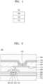
- FIG. 1 is a schematic cross-sectional view of a light-emitting device 10 according to an embodiment.
- the light-emitting device 10 includes a first electrode 110, an interlayer 130, and a second electrode 150.
- a substrate may be additionally located under the first electrode 110 or on the second electrode 150.
- a glass substrate or a plastic substrate may be used as the substrate.
- the substrate may be a flexible substrate, and may include plastics with excellent heat resistance and durability, such as polyimide, polyethylene terephthalate (PET), polycarbonate, polyethylene naphthalate, polyarylate (PAR), polyetherimide, or any combination thereof.
- the first electrode 110 may be formed by, for example, depositing or sputtering a material for forming the first electrode 110 on an upper portion of the substrate.
- a material for forming the first electrode 110 may be a high-work function material that facilitates injection of holes.
- the first electrode 110 may be a reflective electrode, a semi-transmissive electrode, or a transmissive electrode.
- a material for forming the first electrode 110 may include indium tin oxide (ITO), indium zinc oxide (IZO), tin oxide (SnO 2 ), zinc oxide (ZnO), or any combination thereof.
- a material for forming the first electrode 110 may include magnesium (Mg), silver (Ag), aluminium (Al), aluminium-lithium (Al-Li), calcium (Ca), magnesium-indium (Mg-In), magnesium-silver (Mg-Ag), or any combination thereof.
- the first electrode 110 may have a single-layered structure consisting of a single layer or a multi-layered structure including a plurality of layers.
- the first electrode 110 may have a three-layered structure of ITO/Ag/ITO.
- the interlayer 130 may be located on the first electrode 110.
- the interlayer 130 may include an emission layer.
- the interlayer 130 may further include a hole transport region located between the first electrode 110 and the emission layer, and an electron transport region located between the emission layer and the second electrode 150.
- the interlayer 130 may further include, in addition to various organic materials, a metal-containing compound such as an organometallic compound, an inorganic material such as quantum dots, or the like.
- a metal-containing compound such as an organometallic compound, an inorganic material such as quantum dots, or the like.
- the interlayer 130 may include, i) two or more emitting units sequentially stacked between the first electrode 110 and the second electrode 150, and ii) a charge generation layer located between the two or more emitting units.
- the light-emitting device 10 may be a tandem light-emitting device.
- the hole transport region may have: i) a single-layered structure consisting of a single layer consisting of a single material, ii) a single-layered structure consisting of a single layer consisting of a plurality of different materials, or iii) a multi-layered structure including a plurality of layers including different materials.
- the hole transport region may include a hole injection layer, a hole transport layer, an emission auxiliary layer, an electron-blocking layer, or any combination thereof.
- the hole transport region may have a multi-layered structure including a hole injection layer/hole transport layer structure, a hole injection layer/hole transport layer/emission auxiliary layer structure, a hole injection layer/emission auxiliary layer structure, a hole transport layer/emission auxiliary layer structure, or a hole injection layer/hole transport layer/electron-blocking layer structure, the layers of each structure being stacked sequentially from the first electrode 110.
- the hole transport region may include a compound represented by Formula 201, a compound represented by Formula 202, or any combination thereof: wherein, in Formulae 201 and 202,
- each of Formulae 201 and 202 may include at least one of groups represented by Formulae CY201 to CY217: R 10b and R 10c in Formulae CY201 to CY217 are the same as described in connection with R 10a , ring CY 201 to ring CY 204 may each independently be a C 3 -C 20 carbocyclic group or a C 1 -C 20 heterocyclic group, and at least one hydrogen in Formulae CY201 to CY217 may be unsubstituted or substituted with R 10a .
- ring CY 201 to ring CY 204 in Formulae CY201 to CY217 may each independently be a benzene group, a naphthalene group, a phenanthrene group, or an anthracene group.
- each of Formulae 201 and 202 may include at least one of groups represented by Formulae CY201 to CY203.
- Formula 201 may include at least one of the groups represented by Formulae CY201 to CY203 and at least one of the groups represented by Formulae CY204 to CY217.
- xa1 may be 1
- R 201 may be a group represented by one of Formulae CY201 to CY203
- xa2 may be 0
- R 202 may be a group represented by one of Formulae CY204 to CY207.
- each of Formulae 201 and 202 may not include a group represented by one of Formulae CY201 to CY203.
- each of Formulae 201 and 202 may not include a group represented by one of Formulae CY201 to CY203, and may include at least one of the groups represented by Formulae CY204 to CY217.
- each of Formulae 201 and 202 may not include a group represented by one of Formulae CY201 to CY217.
- the hole transport region may include one of Compounds HT1 to HT46, m-MTDATA, TDATA, 2-TNATA, NPB(NPD), ⁇ -NPB, TPD, Spiro-TPD, Spiro-NPB, methylated NPB, TAPC, HMTPD, 4,4',4"-tris(N-carbazolyl)triphenylamine (TCTA), polyaniline/dodecylbenzenesulfonic acid (PANI/DBSA), poly(3,4-ethylenedioxythiophene)/poly(4-styrenesulfonate) (PEDOT/PSS), polyaniline/camphor sulfonic acid (PANI/CSA), polyaniline/poly(4-styrenesulfonate) (PANI/PSS), or any combination thereof:
- a thickness of the hole transport region may be in a range of about 50 ⁇ to about 10,000 ⁇ , for example, about 100 ⁇ to about 4,000 ⁇ .
- a thickness of the hole injection layer may be in a range of about 100 ⁇ to about 9,000 ⁇ , for example, about 100 ⁇ to about 1,000 ⁇
- a thickness of the hole transport layer may be in a range of about 50 ⁇ to about 2,000 ⁇ , for example, about 100 ⁇ to about 1,500 ⁇ .
- the emission auxiliary layer may increase light-emission efficiency by compensating for an optical resonance distance according to the wavelength of light emitted from the emission layer, and the electron-blocking layer may block the leakage of electrons from the emission layer to the hole transport region. Materials that may be included in the hole transport region may be included in the emission auxiliary layer and the electron-blocking layer.
- the hole transport region may further include, in addition to these materials, a charge-generation material for the improvement of conductive properties.
- the charge-generation material may be uniformly or non-uniformly dispersed in the hole transport region (for example, in the form of a single layer consisting of a charge-generation material).
- the charge-generation material may be, for example, a p-dopant.
- the lowest unoccupied molecular orbital (LUMO) energy level of the p-dopant may be -3.5 electron volts (eV) or less.
- the p-dopant may include a quinone derivative, a cyano group-containing compound, a compound including element EL1 and element EL2, or any combination thereof.
- Examples of the quinone derivative are TCNQ, F4-TCNQ, etc.
- Examples of the cyano group-containing compound are HAT-CN, and a compound represented by Formula 221 below.
- Formula 221 HAT-CN, and a compound represented by Formula 221 below.
- element EL1 may be metal, metalloid, or any combination thereof, and element EL2 may be non-metal, metalloid, or any combination thereof.
- the metal examples include an alkali metal (for example, lithium (Li), sodium (Na), potassium (K), rubidium (Rb), cesium (Cs), etc.); alkaline earth metal (for example, beryllium (Be), magnesium (Mg), calcium (Ca), strontium (Sr), barium (Ba), etc.); transition metal (for example, titanium (Ti), zirconium (Zr), hafnium (Hf), vanadium (V), niobium (Nb), tantalum (Ta), chromium (Cr), molybdenum (Mo), tungsten (W), manganese (Mn), technetium (Tc), rhenium (Re), iron (Fe), ruthenium (Ru), osmium (Os), cobalt (Co), rhodium (Rh), iridium (Ir), nickel (Ni), palladium (Pd), platinum (Pt), copper (Cu), silver (Ag), gold (Au), etc
- metalloid examples include silicon (Si), antimony (Sb), and tellurium (Te).
- non-metal examples include oxygen (O) and halogen (for example, F, Cl, Br, I, etc.).
- Examples of the compound including element EL1 and element EL2 are metal oxide, metal halide (for example, metal fluoride, metal chloride, metal bromide, or metal iodide), metalloid halide (for example, metalloid fluoride, metalloid chloride, metalloid bromide, or metalloid iodide), metal telluride, or any combination thereof.
- metal oxide metal halide (for example, metal fluoride, metal chloride, metal bromide, or metal iodide)
- metalloid halide for example, metalloid fluoride, metalloid chloride, metalloid bromide, or metalloid iodide
- metal telluride or any combination thereof.
- metal oxide examples include tungsten oxide (for example, WO, W 2 O 3 , WO 2 , WO 3 , W 2 O 5 , etc.), vanadium oxide (for example, VO, V 2 O 3 , VO 2 , V 2 O 5 , etc.), molybdenum oxide (for example, MoO, Mo 2 O 3 , MoO 2 , MoO 3 , Mo 2 O 5 , etc.), and rhenium oxide (for example, ReO 3 , etc.).
- tungsten oxide for example, WO, W 2 O 3 , WO 2 , WO 3 , W 2 O 5 , etc.
- vanadium oxide for example, VO, V 2 O 3 , VO 2 , V 2 O 5 , etc.
- molybdenum oxide for example, MoO, Mo 2 O 3 , MoO 2 , MoO 3 , Mo 2 O 5 , etc.
- rhenium oxide for example, ReO 3 , etc.
- metal halide examples include alkali metal halide, alkaline earth metal halide, transition metal halide, post-transition metal halide, and lanthanide metal halide.
- alkali metal halide may include LiF, NaF, KF, RbF, CsF, LiCl, NaCl, KCI, RbCl, CsCl, LiBr, NaBr, KBr, RbBr, CsBr, Lil, Nal, KI, Rbl, and Csl.
- alkaline earth metal halide examples include BeF 2 , MgF 2 , CaF 2 , SrF 2 , BaF 2 , BeCl 2 , MgCl 2 , CaCl 2 , SrCl 2 , BaCl 2 , BeBr 2 , MgBr 2 , CaBr 2 , SrBr 2 , BaBr 2 , BeI 2 , MgI 2 , CaI 2 , SrI 2 , and BaI 2 .
- transition metal halide examples include titanium halide (for example, TiF 4 , TiCl 4 , TiBr 4 , TiI 4 , etc.), zirconium halide (for example, ZrF 4 , ZrCl 4 , ZrBr 4 , ZrI 4 , etc.), hafnium halide (for example, HfF 4 , HfCl 4 , HfBr 4 , HfI 4 , etc.), vanadium halide (for example, VF 3 , VCl 3 , VBr 3 , VI 3 , etc.), niobium halide (for example, NbF 3 , NbCl 3 , NbBr 3 , NbI 3 , etc.), tantalum halide (for example, TaF 3 , TaCl 3 , TaBr 3 , TaI 3 , etc.), chromium halide (for example, CrF 3 , CrCl 3 , CrC
- post-transition metal halide examples include zinc halide (for example, ZnF 2 , ZnCl 2 , ZnBr 2 , Znl 2 , etc.), indium halide (for example, InI 3 , etc.), and tin halide (for example, SnI 2 , etc.).
- zinc halide for example, ZnF 2 , ZnCl 2 , ZnBr 2 , Znl 2 , etc.
- indium halide for example, InI 3 , etc.
- tin halide for example, SnI 2 , etc.
- Examples of the lanthanide metal halide are YbF, YbF 2 , YbF 3 , SmF 3 , YbCl, YbCl 2 , YbCl 3 , SmCl 3 , YbBr, YbBr 2 , YbBr 3 , SmBr 3 , Ybl, YbI 2 , YbI 3 , and SmI 3 .
- metalloid halide is antimony halide (for example, SbCl 5 , etc.).
- metal telluride examples include alkali metal telluride (for example, Li 2 Te, Na 2 Te, K 2 Te, Rb 2 Te, Cs 2 Te, etc.), alkaline earth metal telluride (for example, BeTe, MgTe, CaTe, SrTe, BaTe, etc.), transition metal telluride (for example, TiTe 2 , ZrTe 2 , HfTe 2 , V 2 Te 3 , Nb 2 Te 3 , Ta 2 Te 3 , Cr 2 Te 3 , Mo 2 Te 3 , W 2 Te 3 , MnTe, TcTe, ReTe, FeTe, RuTe, OsTe, CoTe, RhTe, IrTe, NiTe, PdTe, PtTe, Cu 2 Te, CuTe, Ag 2 Te, AgTe, Au 2 Te, etc.), post-transition metal telluride (for example, ZnTe, etc.), and lanthanide metal telluride (for example
- the emission layer may be patterned into a red emission layer, a green emission layer, and/or a blue emission layer, according to a sub-pixel.
- the emission layer may have a stacked structure of two or more layers of a red emission layer, a green emission layer, and a blue emission layer, in which the two or more layers contact each other or are separated from each other to emit white light.
- the emission layer may include two or more materials of a red light-emitting material, a green light-emitting material, and a blue light-emitting material, in which the two or more materials are mixed with each other in a single layer to emit white light.
- the emission layer may include a host and a dopant.
- the dopant may include a phosphorescent dopant, a fluorescent dopant, or any combination thereof.
- the amount of the dopant in the emission layer may be from about 0.01 parts by weight to about 15 parts by weight based on 100 parts by weight of the host of the emission layer.
- the emission layer may include the quantum dots.
- the emission layer may include a delayed fluorescence material.
- the delayed fluorescence material may act as a host or a dopant in the emission layer.
- a thickness of the emission layer may be in a range of about 100 ⁇ to about 1,000 ⁇ , for example, about 200 ⁇ to about 600 ⁇ . When the thickness of the emission layer is within these ranges, excellent light-emission characteristics may be obtained without a substantial increase in driving voltage.
- the emission layer may include quantum dots.
- quantum dots refers to crystals of a semiconductor compound and may include any material capable of emitting light of various emission wavelengths according to the particle size of the crystals.
- a diameter of the quantum dot may be, for example, in a range of about 1 nm to about 10 nm.
- the quantum dot may be synthesized by a wet chemical process, a metal organic chemical vapor deposition (MOCVD) process, a molecular beam epitaxy (MBE) process, or any process similar thereto.
- MOCVD metal organic chemical vapor deposition
- MBE molecular beam epitaxy
- the wet chemical process is a method including mixing a precursor material with an organic solvent and then growing a quantum dot particle crystal.
- the organic solvent naturally acts as a dispersant coordinated on the surface of the quantum dot particle crystal and controls the growth of the quantum dot particle crystal so that the growth of quantum dot particle crystals can be controlled with a process that is lower in costs, and is easier than vapor deposition methods, such as metal organic chemical vapor deposition (MOCVD) or molecular beam epitaxy (MBE).
- MOCVD metal organic chemical vapor deposition
- MBE molecular beam epitaxy
- the quantum dot may include Group II-VI semiconductor compounds, Group III-V semiconductor compounds, Group III-VI semiconductor compounds, Group I-III-VI semiconductor compounds, Group IV-VI semiconductor compounds, a Group IV element or compound, or any combination thereof.
- Examples of the Group II-VI semiconductor compound are a binary compound, such as CdS, CdSe, CdTe, ZnS, ZnSe, ZnTe, ZnO, HgS, HgSe, HgTe, MgSe, or MgS; a ternary compound, such as CdSeS, CdSeTe, CdSTe, ZnSeS, ZnSeTe, ZnSTe, HgSeS, HgSeTe, HgSTe, CdZnS, CdZnSe, CdZnTe, CdHgS, CdHgSe, CdHgTe, HgZnS, HgZnSe, HgZnTe, MgZnSe, or MgZnS; a quaternary compound, such as CdZnSeS, CdZnSeTe, CdZnSTe, CdHgSeS, Cd
- Examples of the Group III-V semiconductor compound may include: a binary compound, such as GaN, GaP, GaAs, GaSb, AIN, AlP, AlAs, AlSb, InN, InP, InAs, or InSb; a ternary compound, such as GaNP, GaNAs, GaNSb, GaPAs, GaPSb, AINP, AlNAs, AlNSb, AlPAs, AlPSb, InGaP, InNP, InAlP, InNAs, InNSb, InPAs, or InPSb; a quaternary compound, such as GaAlNP, GaAINAs, GaAINSb, GaAlPAs, GaAlPSb, GalnNP, GalnNAs, GaInNSb, GalnPAs, GalnPSb, InAlNP, InAlNAs, InAlNSb, InAlPAs, or InAlPSb; or any combination thereof. Meanwhile, the Group III-V semiconductor compound may further include a Group II element.
- Group I-III-VI semiconductor compound examples include: a ternary compound, such as AgInS, AgInS 2 , CulnS, CuInS 2 , CuGaO 2 , AgGaO 2 , or AgAlO 2 ; or any combination thereof.
- a ternary compound such as AgInS, AgInS 2 , CulnS, CuInS 2 , CuGaO 2 , AgGaO 2 , or AgAlO 2 ; or any combination thereof.
- Examples of the Group IV-VI semiconductor compound are: a binary compound, such as SnS, SnSe, SnTe, PbS, PbSe, or PbTe; a ternary compound, such as SnSeS, SnSeTe, SnSTe, PbSeS, PbSeTe, PbSTe, SnPbS, SnPbSe, or SnPbTe; a quaternary compound, such as SnPbSSe, SnPbSeTe, or SnPbSTe; or any combination thereof.
- the Group IV element or compound may include: a single element, such as Si or Ge; a binary compound, such as SiC or SiGe; or any combination thereof.
- Each element included in a multi-element compound such as the binary compound, the ternary compound, and the quaternary compound may be present at a uniform concentration or non-uniform concentration in a particle.
- the quantum dot may have a single structure in which the concentration of each element in the quantum dot is uniform, or a core-shell dual structure.
- the material included in the core and the material included in the shell may be different from each other.
- the shell of the quantum dot may act as a protective layer that prevents chemical degeneration, e.g., oxidation, of the core to maintain semiconductor characteristics, and/or as a charging layer that imparts electrophoretic characteristics to the quantum dot.
- the shell may be a single layer or a multi-layer.
- the interface between the core and the shell may have a concentration gradient in which the concentration of an element existing in the shell decreases toward the center of the core.
- Examples of the shell of the quantum dot may be an oxide of a metal, a metalloid, or a non-metal, a semiconductor compound, or any combination thereof.
- Examples of the oxide of metal, metalloid, or non-metal are a binary compound, such as SiO 2 , Al 2 O 3 , TiO 2 , ZnO, MnO, Mn 2 O 3 , Mn 3 O 4 , CuO, FeO, Fe 2 O 3 , Fe 3 O 4 , CoO, Co 3 O 4 , or NiO; a ternary compound, such as MgAl 2 O 4 , CoFe 2 O 4 , NiFe 2 O 4 , or CoMn 2 O 4 ; or any combination thereof.
- the semiconductor compound examples include CdS, CdSe, CdTe, ZnS, ZnSe, ZnTe, ZnSeS, ZnTeS, GaAs, GaP, GaSb, HgS, HgSe, HgTe, InAs, InP, InGaP, InSb, AlAs, AlP, AlSb, or any combination thereof.
- a full width at half maximum (FWHM) of the emission wavelength spectrum of the quantum dot may be about 45 nm or less, for example, about 40 nm or less, for example, about 30 nm or less, and within these ranges, color purity or color reproducibility may be increased..
- the wide viewing angle since the light emitted through the quantum dot is emitted in all directions, the wide viewing angle may be improved.
- the quantum dot may be in the form of a spherical nanoparticle, a pyramidal nanoparticle, a multi-arm nanoparticle, a cubic nanoparticle, a nanotube, a nanowire, a nanofiber, or a nanoplate.
- the energy band gap may be adjusted by controlling the size of the quantum dot
- light having various wavelength bands may be obtained from the quantum dot emission layer. Accordingly, by using quantum dots of different sizes, a light-emitting device that emits light of various wavelength bands may be implemented.
- the size of the quantum dot may be selected to emit red, green and/or blue light.
- the size of the quantum dot may be configured to emit white light by combination of light of various colors.
- Electron transport region in interlayer 130 is Electron transport region in interlayer 130
- the electron transport region may have: i) a single-layered structure consisting of a single layer consisting of a single material, ii) a single-layered structure consisting of a single layer consisting of a plurality of different materials, or iii) a multi-layered structure including a plurality of layers including different materials.
- the electron transport region may include a hole-blocking layer, an electron transport layer, an electron injection layer, or any combination thereof.
- the electron transport region may have an electron transport layer/electron injection layer structure or a hole-blocking layer/electron transport layer/electron injection layer structure, wherein, in each structure, constituting layers are sequentially stacked from the emission layer.
- the electron transport region (for example, the hole-blocking layer, or the electron transport layer in the electron transport region) may include a metal-free compound including at least one ⁇ electron-deficient nitrogen-containing C 1 -C 60 cyclic group.
- the electron transport region may include a compound represented by Formula 601 below: Formula 601 [Ar 601 ] xe11 -(L 601 ) xe1 -R 601 ] xe21 wherein, in Formula 601,
- xe11 in Formula 601 is 2 or more
- two or more of Ar 601 (s) may be linked to each other via a single bond.
- Ar 601 in Formula 601 may be a substituted or unsubstituted anthracene group unsubstituted or substituted with at least one R 10a .
- the electron transport region may include a compound represented by Formula 601-1: wherein, in Formula 601-1,
- xe1 and xe611 to xe613 in Formulae 601 and 601-1 may each independently be 0, 1, or 2.
- the electron transport region may include one of Compounds ET1 to ET45, 2,9-dimethyl-4,7-diphenyl-1,10-phenanthroline (BCP), 4,7-diphenyl-1,10-phenanthroline (Bphen), Alq 3 , BAlq, TAZ, NTAZ, or any combination thereof:
- a thickness of the electron transport region may be from about 100 ⁇ to about 5,000 ⁇ , for example, about 160 ⁇ to about 4,000 ⁇ .
- a thickness of the hole blocking layer may be from about 20 ⁇ to about 1,000 ⁇ , for example, about 30 ⁇ to about 300 ⁇ , and the thickness of the electron transport layer may be from about 100 ⁇ to about 1,000 ⁇ , for example, about 150 ⁇ to about 500 ⁇ .
- the thicknesses of the hole blocking layer and/or the electron transport layer are within these ranges, satisfactory electron transporting characteristics may be obtained without a substantial increase in driving voltage.
- the electron transport region (for example, the electron transport layer in the electron transport region) may further include, in addition to the materials described above, a metal-containing material.
- the metal-containing material may include an alkali metal complex, an alkaline earth metal complex, or any combination thereof.
- the metal ion of an alkali metal complex may be a Li ion, a Na ion, a K ion, a Rb ion, or a Cs ion
- the metal ion of an alkaline earth metal complex may be a Be ion, a Mg ion, a Ca ion, a Sr ion, or a Ba ion.
- a ligand coordinated with the metal ion of the alkali metal complex or the alkaline earth-metal complex may include a hydroxyquinoline, a hydroxyisoquinoline, a hydroxybenzoquinoline, a hydroxyacridine, a hydroxyphenanthridine, a hydroxyphenyloxazole, a hydroxyphenylthiazole, a hydroxyphenyloxadiazole, a hydroxyphenylthiadiazole, a hydroxyphenylpyridine, a hydroxyphenylbenzimidazole, a hydroxyphenylbenzothiazole, a bipyridine, a phenanthroline, a cyclopentadiene, or any combination thereof.
- the metal-containing material may include a Li complex.
- the Li complex may include, for example, Compound ET-D1 (Liq) or ET-D2:
- the electron transport region may include an electron injection layer that facilitates the injection of electrons from the second electrode 150.
- the electron injection layer may directly contact the second electrode 150.
- the electron injection layer may have: i) a single-layered structure consisting of a single layer consisting of a single material, ii) a single-layered structure consisting of a single layer consisting of a plurality of different materials, or iii) a multi-layered structure including a plurality of layers including different materials.
- the electron injection layer may include an alkali metal, alkaline earth metal, a rare earth metal, an alkali metal-containing compound, alkaline earth metal-containing compound, a rare earth metal-containing compound, an alkali metal complex, an alkaline earth metal complex, a rare earth metal complex, or any combination thereof.
- the alkali metal may include Li, Na, K, Rb, Cs, or any combination thereof.
- the alkaline earth metal may include Mg, Ca, Sr, Ba, or any combination thereof.
- the rare earth metal may include Sc, Y, Ce, Tb, Yb, Gd, or any combination thereof.
- the alkali metal-containing compound, the alkaline earth metal-containing compound, and the rare earth metal-containing compound may be oxides, halides (for example, fluorides, chlorides, bromides, or iodides), or tellurides of the alkali metal, the alkaline earth metal, and the rare earth metal, or any combination thereof.
- the alkali metal-containing compound may include alkali metal oxides, such as Li 2 O, Cs 2 O, or K 2 O; alkali metal halides, such as LiF, NaF, CsF, KF, Lil, Nal, Csl, or KI; or any combination thereof.
- the alkaline earth metal-containing compound may include an alkaline earth metal oxide, such as BaO, SrO, CaO, Ba x Sr 1-x O (wherein x is a real number satisfying the condition of 0 ⁇ x ⁇ 1), Ba x Ca 1-x O (wherein x is a real number satisfying the condition of 0 ⁇ x ⁇ 1), or the like.
- the rare earth metal-containing compound may include YbF 3 , ScF 3 , Sc 2 O 3 , Y 2 O 3 , Ce 2 O 3 , GdF 3 , TbF 3 , YbI 3 , ScI 3 , TbI 3 , or any combination thereof.
- the rare earth metal-containing compound may include lanthanide metal telluride.
- Examples of the lanthanide metal telluride are LaTe, CeTe, PrTe, NdTe, PmTe, SmTe, EuTe, GdTe, TbTe, DyTe, HoTe, ErTe, TmTe, YbTe, LuTe, La 2 Te 3 , Ce 2 Te 3 , Pr 2 Te 3 , Nd 2 Te 3 , Pm 2 Te 3 , Sm 2 Te 3 , Eu 2 Te 3 , Gd 2 Te 3 , Tb 2 Te 3 , Dy 2 Te 3 , Ho 2 Te 3 , Er 2 Te 3 , Tm 2 Te 3 , Yb 2 Te 3 , and Lu 2 Te 3 .
- the alkali metal complex, the alkaline earth-metal complex, and the rare earth metal complex may include i) one of ions of the alkali metal, the alkaline earth metal, and the rare earth metal and ii), as a ligand bonded to the metal ion, for example, a hydroxyquinoline, a hydroxyisoquinoline, a hydroxybenzoquinoline, a hydroxyacridine, a hydroxyphenanthridine, a hydroxyphenyloxazole, a hydroxyphenylthiazole, a hydroxyphenyloxadiazole, a hydroxyphenylthiadiazole, a hydroxyphenylpyridine, a hydroxyphenyl benzimidazole, a hydroxyphenylbenzothiazole, a bipyridine, a phenanthroline, a cyclopentadiene, or any combination thereof.
- the electron injection layer may consist of an alkali metal, an alkaline earth metal, a rare earth metal, an alkali metal-containing compound, an alkaline earth metal-containing compound, a rare earth metal-containing compound, an alkali metal complex, an alkaline earth metal complex, a rare earth metal complex, or any combination thereof, as described above.
- the electron injection layer may further include an organic material (for example, a compound represented by Formula 601).
- the electron injection layer may consist of: i) an alkali metal-containing compound (for example, an alkali metal halide); or ii) a) an alkali metal-containing compound (for example, an alkali metal halide), and b) an alkali metal, an alkaline earth metal, a rare earth metal, or any combination thereof.
- the electron injection layer may be a KI:Yb co-deposited layer, an Rbl:Yb co-deposited layer, or the like.
- an alkali metal, an alkaline earth metal, a rare earth metal, an alkali metal-containing compound, an alkaline earth metal-containing compound, a rare earth metal-containing compound, an alkali metal complex, an alkaline earth-metal complex, a rare earth metal complex, or any combination thereof may be uniformly or non-uniformly dispersed in a matrix including the organic material.
- a thickness of the electron injection layer may be in a range of about 1 ⁇ to about 100 ⁇ , for example, about 3 ⁇ to about 90 ⁇ . When the thickness of the electron injection layer is within the ranges described above, satisfactory electron injection characteristics may be obtained without a substantial increase in driving voltage.
- the second electrode 150 may be located on the interlayer 130 having a structure as described above.
- the second electrode 150 may be a cathode, which is an electron injection electrode, and as the material for the second electrode 150, a metal, an alloy, an electrically conductive compound, or any combination thereof, each having a low-work function, may be used.
- the second electrode 150 may include lithium (Li), silver (Ag), magnesium (Mg), aluminium (Al), aluminium-lithium (Al-Li), calcium (Ca), magnesium-indium (Mg-In), magnesium-silver (Mg-Ag), ytterbium (Yb), silver-ytterbium (Ag-Yb), ITO, IZO, or any combination thereof.
- the second electrode 150 may be a transmissive electrode, a semi-transmissive electrode, or a reflective electrode.
- the second electrode 150 may have a single-layered structure or a multi-layered structure including a plurality of layers.
- a first capping layer may be located outside the first electrode 110, and/or a second capping layer may be located outside the second electrode 150.
- the light-emitting device 10 may have a structure in which the first capping layer, the first electrode 110, the interlayer 130, and the second electrode 150 are sequentially stacked in the stated order, a structure in which the first electrode 110, the interlayer 130, the second electrode 150, and the second capping layer are sequentially stacked in the stated order, or a structure in which the first capping layer, the first electrode 110, the interlayer 130, the second electrode 150, and the second capping layer are sequentially stacked in the stated order.
- Light generated in an emission layer of the interlayer 130 of the light-emitting device 10 may be extracted toward the outside through the first electrode 110 which is a semi-transmissive electrode or a transmissive electrode, and the first capping layer.
- Light generated in an emission layer of the interlayer 130 of the light-emitting device 10 may be extracted toward the outside through the second electrode 150 which is a semi-transmissive electrode or a transmissive electrode, and the second capping layer.
- the first capping layer and the second capping layer may increase external emission efficiency according to the principle of constructive interference. Accordingly, the light extraction efficiency of the light-emitting device 10 is increased, so that the luminescence efficiency of the light-emitting device 10 may be improved.
- Each of the first capping layer and the second capping layer may include a material having a refractive index of 1.6 or more (at 589 nm).
- the first capping layer and the second capping layer may each independently be an organic capping layer including an organic material, an inorganic capping layer including an inorganic material, or an organic-inorganic composite capping layer including an organic material and an inorganic material.
- At least one of the first capping layer and the second capping layer may each independently include carbocyclic compounds, heterocyclic compounds, amine group-containing compounds, porphine derivatives, phthalocyanine derivatives, naphthalocyanine derivatives, alkali metal complexes, alkaline earth metal complexes, or any combination thereof.
- the carbocyclic compound, the heterocyclic compound, and the amine group-containing compound may be substituted with a substituent including O, N, S, Se, Si, F, CI, Br, I, or any combination thereof.
- at least one of the first capping layer and the second capping layer may each independently include an amine group-containing compound.
- At least one of the first capping layer and the second capping layer may each independently include a compound represented by Formula 201, a compound represented by Formula 202, or any combination thereof.
- At least one of the first capping layer and the second capping layer may each independently include one of Compounds HT28 to HT33, one of Compounds CP1 to CP6, ⁇ -NPB, or any combination thereof:
- the light-emitting device may be included in various electronic apparatuses.
- the electronic apparatus including the light-emitting device may be a light-emitting apparatus, an authentication apparatus, or the like.
- the electronic apparatus may further include, in addition to the light-emitting device, i) a color filter, ii) a color conversion layer, or iii) a color filter and a color conversion layer.
- the color filter and/or the color conversion layer may be located in at least one direction in which light emitted from the light-emitting device travels.
- the light emitted from the light-emitting device may be blue light or white light.
- related description provided above may be referred to.
- the electronic apparatus may include a first substrate.
- the first substrate may include a plurality of subpixel areas
- the color filter may include a plurality of color filter areas respectively corresponding to the plurality of subpixel areas
- the color conversion layer may include a plurality of color conversion areas respectively corresponding to the plurality of subpixel areas.
- a pixel defining layer may be located among the plurality of subpixel areas to define each of the plurality of subpixel areas.
- the color filter may further include a plurality of color filter areas and light-shielding patterns located among the plurality of color filter areas
- the color conversion layer may further include a plurality of color conversion areas and light-shielding patterns located among the plurality of color conversion areas.
- the plurality of color filter areas may include a first area emitting first color light, a second area emitting second color light, and/or a third area emitting third color light, wherein the first color light, the second color light, and/or the third color light may have different maximum emission wavelengths from one another.
- the first color light may be red light
- the second color light may be green light
- the third color light may be blue light.
- the plurality of color filter areas (or the plurality of color conversion areas) may include quantum dots.
- the first area may include a red quantum dot
- the second area may include a green quantum dot
- the third area may not include a quantum dot.
- the first area, the second area, and/or the third area may each include a scatterer.
- the areas including quantum dots may be formed using a composition including quantum dots coordinated with the compound as described herein.
- the light-emitting device may emit a first light
- the first area may absorb the first light to emit first-first color light
- the second area may absorb the first light to emit second-first color light
- the third area may absorb the first light to emit third-first color light.
- the first-first color light, the second-first color light, and the third-first color light may have different maximum emission wavelengths.
- the first light may be blue light
- the first-first color light may be red light
- the second-first color light may be green light
- the third-first color light may be blue light.
- the electronic apparatus may further include a thin-film transistor, in addition to the light-emitting device as described above.
- the thin-film transistor may include a source electrode, a drain electrode, and an activation layer, wherein any one of the source electrode and the drain electrode may be electrically connected to any one of the first electrode and the second electrode of the light-emitting device.
- the thin-film transistor may further include a gate electrode, a gate insulating film, or the like.
- the activation layer may include crystalline silicon, amorphous silicon, an organic semiconductor, an oxide semiconductor, or the like.
- the electronic apparatus may further include a sealing portion for sealing the light-emitting device.
- the sealing portion may be located between the color filter and/or the color conversion layer and the light-emitting device.
- the sealing portion allows light from the light-emitting device to be extracted to the outside, and simultaneously prevents ambient air and moisture from penetrating into the light-emitting device.
- the sealing portion may be a sealing substrate including a transparent glass substrate or a plastic substrate.
- the sealing portion may be a thin-film encapsulation layer including at least one layer of an organic layer and an inorganic layer. When the sealing portion is a thin film encapsulation layer, the electronic apparatus may be flexible.
- the authentication apparatus may further include, in addition to the light-emitting device as described above, a biometric information collector.
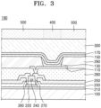
- a TFT may be located on the buffer layer 210.
- the TFT may include an activation layer 220, a gate electrode 240, a source electrode 260, and a drain electrode 270.
- An interlayer insulating film 250 may be located on the gate electrode 240.
- the interlayer insulating film 250 may be located between the gate electrode 240 and the source electrode 260 and between the gate electrode 240 and the drain electrode 270, to insulate from one another.
- the source electrode 260 and the drain electrode 270 may be located on the interlayer insulating film 250.
- the interlayer insulating film 250 and the gate insulating film 230 may be formed to expose the source region and the drain region of the activation layer 220, and the source electrode 260 and the drain electrode 270 may be located in contact with the exposed portions of the source region and the drain region of the activation layer 220.
- the first electrode 110 may be located on the passivation layer 280.
- the passivation layer 280 may be located to expose a portion of the drain electrode 270, not fully covering the drain electrode 270, and the first electrode 110 may be located to be connected to the exposed portion of the drain electrode 270.
- a pixel defining layer 290 including an insulating material may be located on the first electrode 110.
- the pixel defining layer 290 may expose a certain region of the first electrode 110, and an interlayer 130 may be formed in the exposed region of the first electrode 110.
- the pixel defining layer 290 may be a polyimide or polyacrylic organic film.
- at least some layers of the interlayer 130 may extend beyond the upper portion of the pixel defining layer 290 to be located in the form of a common layer.
- the second electrode 150 may be located on the interlayer 130, and a capping layer 170 may be additionally formed on the second electrode 150.
- the capping layer 170 may be formed to cover the second electrode 150.
- the encapsulation portion 300 may be located on the capping layer 170.
- the encapsulation portion 300 may be located on a light-emitting device to protect the light-emitting device from moisture or oxygen.
- the encapsulation portion 300 may include: an inorganic film including silicon nitride (SiN x ), silicon oxide (SiO x ), indium tin oxide, indium zinc oxide, or any combination thereof; an organic film including polyethylene terephthalate, polyethylene naphthalate, polycarbonate, polyimide, polyethylene sulfonate, polyoxymethylene, polyarylate, hexamethyldisiloxane, an acrylic-based resin (for example, polymethyl methacrylate, polyacrylic acid, or the like), an epoxy-based resin (for example, aliphatic glycidyl ether (AGE), or the like), or any combination thereof; or any combination of the inorganic films and the organic films.
- an inorganic film including silicon nit
- Respective layers included in the hole transport region, the emission layer, and respective layers included in the electron transport region may be formed in a certain region by using one or more suitable methods selected from vacuum deposition, spin coating, casting, Langmuir-Blodgett (LB) deposition, ink-jet printing, laser-printing, laser-induced thermal imaging (LITI), and the like.
- suitable methods selected from vacuum deposition, spin coating, casting, Langmuir-Blodgett (LB) deposition, ink-jet printing, laser-printing, laser-induced thermal imaging (LITI), and the like.
- the color filter area, the color conversion area, etc. may be formed in a certain region using a spin coating method, a casting method, an ink jet printing method, or the like.
- the deposition may be performed at a deposition temperature of about 100 °C to about 500 °C, a vacuum degree of about 10 -8 torr to about 10 -3 torr, and a deposition speed of about 0.01 angstroms per second ( ⁇ /sec) to about 100 ⁇ /sec, depending on a material to be included in a layer to be formed and the structure of a layer to be formed.
- the spin coating may be performed at a coating speed of about 2,000 rpm to about 5,000 rpm and at a heat treatment temperature of about 80 °C to about 200 °C by taking into account a material to be included in a layer to be formed and the structure of a layer to be formed.
- composition according to an embodiment may be used in a solution process such as a spin coating method or an inkjet printing method.
- C 3 -C 60 carbocyclic group refers to a cyclic group consisting of carbon atoms only as a ring-forming atom and having three to sixty carbon atoms
- C 1 -C 60 heterocyclic group refers to a cyclic group that has one to sixty carbon atoms and further has, in addition to carbon atoms, a heteroatom as a ring-forming atom.
- the C 3 -C 60 carbocyclic group and the C 1 -C 60 heterocyclic group may each be a monocyclic group consisting of one ring or a polycyclic group in which two or more rings are condensed with each other.
- the C 1 -C 60 heterocyclic group has 3 to 61 ring-forming atoms.
- cyclic group as used herein may include the C 3 -C 60 carbocyclic group, and the C 1 -C 60 heterocyclic group.
- C 1 -C 60 alkyl group refers to a linear or branched aliphatic hydrocarbon monovalent group that has one to sixty carbon atoms, and specific examples thereof are a methyl group, an ethyl group, an n-propyl group, an isopropyl group, an n-butyl group, a sec-butyl group, an isobutyl group, a tert-butyl group, an n-pentyl group, a tert-pentyl group, a neopentyl group, an isopentyl group, a sec-pentyl group, a 3-pentyl group, a sec-isopentyl group, an n-hexyl group, an isohexyl group, a sec-hexyl group, a tert-hexyl group, an n-heptyl group, an isoheptyl group, a sec-
- C 2 -C 60 alkenyl group refers to a monovalent hydrocarbon group having at least one carbon-carbon double bond in the middle or at the terminus of the C 2 -C 60 alkyl group, and examples thereof are an ethenyl group, a propenyl group, and a butenyl group.
- C 2 -C 60 alkenylene group refers to a divalent group having the same structure as the C 2 -C 60 alkenyl group.
- C 1 -C 60 alkoxy group refers to a monovalent group represented by -OA 101 (wherein A 101 is the C 1 -C 60 alkyl group), and examples thereof include a methoxy group, an ethoxy group, and an isopropyloxy group.
- C 3 -C 10 cycloalkyl group refers to a monovalent saturated hydrocarbon cyclic group having 3 to 10 carbon atoms, and examples thereof are a cyclopropyl group, a cyclobutyl group, a cyclopentyl group, a cyclohexyl group, a cycloheptyl group, a cyclooctyl group, an adamantanyl group, a norbornyl group (or bicyclo[2.2.1]heptyl group), a bicyclo[1.1.1]pentyl group, a bicyclo[2.1.1]hexyl group, and a bicyclo[2.2.2]octyl group.
- C 3 -C 10 cycloalkylene group refers to a divalent group having the same structure as the C 3 -C 10 cycloalkyl group.
- C 3 -C 10 cycloalkenyl group used herein refers to a monovalent cyclic group that has three to ten carbon atoms and at least one carbon-carbon double bond in the ring thereof and no aromaticity, and specific examples thereof are a cyclopentenyl group, a cyclohexenyl group, and a cycloheptenyl group.
- C 3 -C 10 cycloalkenylene group refers to a divalent group having the same structure as the C 3 -C 10 cycloalkenyl group.
- C 1 -C 10 heterocycloalkenyl group refers to a monovalent cyclic group of 1 to 10 carbon atoms, further including, in addition to carbon atoms, at least one heteroatom, as ring-forming atoms, and having at least one double bond in the cyclic structure thereof.
- Examples of the C 1 -C 10 heterocycloalkenyl group include a 4,5-dihydro-1,2,3,4-oxatriazolyl group, a 2,3-dihydrofuranyl group, and a 2,3-dihydrothienyl group.
- C 1 -C 10 heterocycloalkenylene group refers to a divalent group having the same structure as the C 1 -C 10 heterocycloalkenyl group.
- C 6 -C 60 aryl group refers to a monovalent group having a carbocyclic aromatic system of 6 to 60 ring carbon atoms
- C 6 -C 60 arylene group refers to a divalent group having a carbocyclic aromatic system of 6 to 60 carbon ring atoms.
- the term "monovalent non-aromatic condensed polycyclic group” as used herein refers to a monovalent group (for example, having 8 to 60 carbon ring atoms) having two or more rings condensed to each other, only carbon atoms as ring-forming atoms, and no aromaticity in its entire molecular structure.
- Examples of the monovalent non-aromatic condensed polycyclic group are an indenyl group, a fluorenyl group, a spiro-bifluorenyl group, a benzofluorenyl group, an indenophenanthrenyl group, and an indeno anthracenyl group.
- divalent non-aromatic condensed polycyclic group refers to a divalent group having the same structure as the monovalent non-aromatic condensed polycyclic group described above.
- monovalent non-aromatic condensed heteropolycyclic group refers to a monovalent group (for example, having 1 to 60 carbon atoms) having two or more rings condensed to each other, further including, in addition to carbon atoms, at least one heteroatom, as ring-forming atoms, and having non-aromaticity in its entire molecular structure.
- Examples of the monovalent non-aromatic condensed heteropolycyclic group include a pyrrolyl group, a thienyl group, a furanyl group, an indolyl group, a benzoindolyl group, a naphtho indolyl group, an isoindolyl group, a benzoisoindolyl group, a naphthoisoindolyl group, a benzosilolyl group, a benzothienyl group, a benzofuranyl group, a carbazolyl group, a dibenzosilolyl group, a dibenzothienyl group, a dibenzofuranyl group, an azacarbazolyl group, an azafluorenyl group, an azadibenzosilolyl group, an azadibenzothienyl group, an azadibenzofuranyl group, a pyrazolyl group,
- C 7 -C 60 aryl alkyl group used herein refers to -A 104 A 105 (where A 104 may be a C 1 -C 54 alkylene group, and A 105 may be a C 6 -C 59 aryl group), and the term C 2 -C 60 heteroaryl alkyl group” used herein refers to -A 106 A 107 (where A 106 may be a C 1 -C 59 alkylene group, and A 107 may be a C 1 -C 59 heteroaryl group).
- R 10a refers to:
- Ph refers to a phenyl group
- Me refers to a methyl group
- Et refers to an ethyl group
- tert-Bu refers to a tert-butyl group
- OMe refers to a methoxy group
- biphenyl group refers to "a phenyl group substituted with a phenyl group.”
- the "biphenyl group” is a substituted phenyl group having a C 6 -C 60 aryl group as a substituent.
- terphenyl group refers to "a phenyl group substituted with a biphenyl group”.
- the "terphenyl group” is a substituted phenyl group having, as a substituent, a C 6 -C 60 aryl group substituted with a C 6 -C 60 aryl group.
- the maximum number of carbon atoms in this substituent definition section is an example only.
- the maximum carbon number of 60 in the C 1 -C 60 alkyl group is an example, and the definition of the alkyl group is equally applied to a C 1 -C 20 alkyl group. The same applies to other cases.
- Compound 2 was obtained in substantially the same manner as Example 1 was obtained except that 170 g of triethylene glycol monophenyl ether was used instead of tetraethylene glycol monophenyl ether.
- Compound 3 was obtained in substantially the same manner as Example 1 was obtained except that 200 g of triethylene glycol monophenyl ether was used instead of tetraethylene glycol monophenyl ether.
- Compound 4 was obtained in substantially the same manner as Example 1 was obtained except that 200 g of triethylene glycol monobutyl ether was used instead of tetraethylene glycol monophenyl ether.
- Compound 5 was obtained in substantially the same manner as Example 1 was obtained except that 200 g of triethylene glycol monobenzyl ether was used instead of tetraethylene glycol monophenyl ether.
- compositions were manufacturing using the quantum dots and ligands of Table 1.
- Table 1 Quantum dot (10 nm) Ligand Comparative Example 1 ZnS shell and Group II-V core Compound 101 Comparative Example 2 ZnS shell and Group II-V core Compound 102 Comparative Example 3 ZnS shell and Group III-V core Compound 103 Comparative Example 4 ZnS shell and Group III-V core Compound 104 Comparative Example 5 ZnS shell and Group II-V core Compound 105
- Example 6 ZnS shell and Group II-V core Compound 1
- Example 10 ZnS shell and Group II-V core Compound 5
- a composition was manufactured in substantially the same manner as in Comparative Example 1 except that 0.374 g of Compound 102 was used instead of Compound 101.
- a composition was manufactured in substantially the same manner as in Comparative Example 1 except that 0.377 g of Compound 103 was used instead of Compound 101.
- a composition was manufactured in substantially the same manner as in Comparative Example 1 except that 0.508 g of Compound 104 was used instead of Compound 101.
- a composition was manufactured in substantially the same manner as in Comparative Example 1 except that 0.339 g of Compound 105 was used instead of Compound 101.
- a composition was manufactured in substantially the same manner as in Comparative Example 1 except that 0.489 g of Compound 1 was used instead of Compound 101.
- a composition was manufactured in substantially the same manner as in Comparative Example 1 except that 0.396 g of Compound 2 was used instead of Compound 101.
- a composition was manufactured in substantially the same manner as in Comparative Example 1 except that 0.442 g of Compound 3 was used instead of Compound 101.
- a composition was manufactured in substantially the same manner as in Comparative Example 1 except that 0.421 g of Compound 4 was used instead of Compound 101.
- a composition was manufactured in substantially the same manner as in Comparative Example 1 except that 0.457 g of Compound 5 was used instead of Compound 101.
- the initial viscosity (at 25 °C) of the comparative examples and examples was about 25 centipoise (cP) to about 30 cP.
- Comparative Example 1 The composition of Comparative Example 1 was spin-coated on a glass to a thickness of 10 ⁇ m and exposed to UV (360 nm max ) to prepare a color conversion layer specimen.
- a specimen was prepared in substantially the same manner as in Comparative Example 6, except that the quantum dot compositions of Examples 6 to 10 were used for each of the color conversion layers.
Landscapes
- Chemical & Material Sciences (AREA)
- Organic Chemistry (AREA)
- Engineering & Computer Science (AREA)
- Materials Engineering (AREA)
- Inorganic Chemistry (AREA)
- Physics & Mathematics (AREA)
- Health & Medical Sciences (AREA)
- Chemical Kinetics & Catalysis (AREA)
- Medicinal Chemistry (AREA)
- Polymers & Plastics (AREA)
- Optics & Photonics (AREA)
- Nanotechnology (AREA)
- Crystallography & Structural Chemistry (AREA)
- Spectroscopy & Molecular Physics (AREA)
- Luminescent Compositions (AREA)
- Electroluminescent Light Sources (AREA)
- Organic Low-Molecular-Weight Compounds And Preparation Thereof (AREA)
- Devices For Indicating Variable Information By Combining Individual Elements (AREA)
Applications Claiming Priority (2)
| Application Number | Priority Date | Filing Date | Title |
|---|---|---|---|
| KR1020220049103A KR20230149911A (ko) | 2022-04-20 | 2022-04-20 | 화합물, 이로 배위된 양자점, 이를 포함하는 조성물 및 이를 사용하여 제조된 전자 장치 |
| PCT/KR2023/005376 WO2023204627A1 (ko) | 2022-04-20 | 2023-04-20 | 화합물, 이로 배위된 양자점, 이를 포함하는 조성물 및 이를 사용하여 제조된 전자 장치 |
Publications (2)
| Publication Number | Publication Date |
|---|---|
| EP4512799A1 true EP4512799A1 (de) | 2025-02-26 |
| EP4512799A4 EP4512799A4 (de) | 2026-02-18 |
Family
ID=88416116
Family Applications (1)
| Application Number | Title | Priority Date | Filing Date |
|---|---|---|---|
| EP23792201.8A Pending EP4512799A4 (de) | 2022-04-20 | 2023-04-20 | Verbindung, damit koordinierte quantenpunkte, zusammensetzung damit und unter verwendung davon hergestellte elektronische vorrichtung |
Country Status (6)
| Country | Link |
|---|---|
| US (1) | US20230340322A1 (de) |
| EP (1) | EP4512799A4 (de) |
| JP (1) | JP2025517059A (de) |
| KR (1) | KR20230149911A (de) |
| CN (1) | CN118946546A (de) |
| WO (1) | WO2023204627A1 (de) |
Families Citing this family (2)
| Publication number | Priority date | Publication date | Assignee | Title |
|---|---|---|---|---|
| US20240172463A1 (en) * | 2021-05-31 | 2024-05-23 | Beijing Boe Technology Development Co., Ltd. | Quantum Dot Material and Preparation Method thereof, Quantum Dot Display Device, and Display Apparatus |
| KR20250114190A (ko) * | 2024-01-19 | 2025-07-29 | 삼성디스플레이 주식회사 | 양자점 복합체, 이를 포함한 양자점 조성물 및 이를 포함한 전자 장치 |
Family Cites Families (4)
| Publication number | Priority date | Publication date | Assignee | Title |
|---|---|---|---|---|
| CN110858632B (zh) * | 2018-08-23 | 2024-07-12 | 三星电子株式会社 | 量子点器件和量子点 |
| KR20210021666A (ko) * | 2019-08-19 | 2021-03-02 | 주식회사 앤아이씨연구소 | 경화성 양자점 리간드 |
| KR20210021897A (ko) * | 2019-08-19 | 2021-03-02 | 주식회사 앤아이씨연구소 | 광가교성 양자점리간드 |
| KR20210149971A (ko) * | 2020-06-02 | 2021-12-10 | 삼성디스플레이 주식회사 | 양자점 조성물, 발광 소자 및 이를 포함하는 표시 장치 |
-
2022
- 2022-04-20 KR KR1020220049103A patent/KR20230149911A/ko active Pending
-
2023
- 2023-02-07 US US18/165,496 patent/US20230340322A1/en active Pending
- 2023-04-20 JP JP2024560523A patent/JP2025517059A/ja active Pending
- 2023-04-20 CN CN202380030343.XA patent/CN118946546A/zh active Pending
- 2023-04-20 WO PCT/KR2023/005376 patent/WO2023204627A1/ko not_active Ceased
- 2023-04-20 EP EP23792201.8A patent/EP4512799A4/de active Pending
Also Published As
| Publication number | Publication date |
|---|---|
| KR20230149911A (ko) | 2023-10-30 |
| CN118946546A (zh) | 2024-11-12 |
| US20230340322A1 (en) | 2023-10-26 |
| WO2023204627A1 (ko) | 2023-10-26 |
| EP4512799A4 (de) | 2026-02-18 |
| JP2025517059A (ja) | 2025-06-03 |
Similar Documents
| Publication | Publication Date | Title |
|---|---|---|
| KR102862545B1 (ko) | 발광 소자 및 이의 제조 방법 | |
| KR102895952B1 (ko) | 양자점-함유 물질, 상기 양자점-함유 물질의 제조 방법, 상기 양자점-함유 물질의 가교-결합물, 상기 가교-결합물의 제조 방법 및 상기 가교-결합물을 포함하는 발광 소자 | |
| US11802239B2 (en) | Quantum dot, method of preparing quantum dot, optical member including quantum dot, and electronic device including quantum dot | |
| CN116265567A (zh) | 含量子点配合物、墨组合物、发光器件和电子设备 | |
| EP4512799A1 (de) | Verbindung, damit koordinierte quantenpunkte, zusammensetzung damit und unter verwendung davon hergestellte elektronische vorrichtung | |
| US20240279538A1 (en) | Quantum dot-containing complex, quantum dot composition including the same, and electronic apparatus including the same | |
| EP4468844A1 (de) | Quantenpunktzusammensetzung, lichtemittierende vorrichtung damit und elektronische vorrichtung mit der lichtemittierenden vorrichtung | |
| US20230354631A1 (en) | Quantum dot composition, light-emitting device using the quantum dot composition, and electronic apparatus including the light-emitting device | |
| KR102929418B1 (ko) | 발광 소자 및 이를 포함하는 전자 장치 | |
| CN117887446A (zh) | 含量子点复合物及其制造方法、发光装置和电子设备 | |
| CN116347911A (zh) | 发光装置及包括发光装置的电子设备 | |
| CN116249365A (zh) | 包括杂环化合物的发光器件和包括发光器件的电子设备 | |
| KR20240029638A (ko) | 양자점 잉크 조성물용 혼합 용매, 이를 포함하는 양자점 잉크 조성물, 이를 사용하여 제조된 발광 소자 및 이를 포함하는 전자 장치 | |
| KR20230126308A (ko) | 발광 소자용 잉크 조성물 및 이를 사용하여 제조된 발광 소자 | |
| EP4223852B1 (de) | Quantenpunkt, verfahren zur herstellung des quantenpunkts und elektronische vorrichtung mit dem quantenpunkt | |
| EP4468843A1 (de) | Lichtemittierende vorrichtung mit quantenpunkten und elektronische vorrichtung mit der lichtemittierenden vorrichtung | |
| US20230403875A1 (en) | Method of preparing quantum dot, quantum dot prepared thereby, and optical member and electronic apparatus including the quantum dot | |
| US20250236791A1 (en) | Quantum dot complex, quantum dot composition including the same, and electronic apparatus including the quantum dot complex | |
| US20240279168A1 (en) | Ligand compound and inorganic nanoparticle-complex including the same | |
| CN114561212B (zh) | 含有量子点的材料、其制备方法、组合物以及发光器件 | |
| KR102914862B1 (ko) | 유기금속 화합물을 포함한 발광 소자, 상기 발광 소자를 포함한 전자 장치 및 상기 유기금속 화합물 | |
| US20230227718A1 (en) | Metal oxide composition, light-emitting device using the metal oxide composition, and electronic apparatus including the light-emitting device | |
| US20230371296A1 (en) | Quantum dot composition, light-emitting device including the quantum dot composition, and electronic apparatus including the light-emitting device | |
| US20230240142A1 (en) | Condensed cyclic compound, light-emitting device including the same, and electronic apparatus including the light-emitting device | |
| US20220384752A1 (en) | Method of preparing quantum dots, quantum dot prepared by the method of preparing quantum dot, optical member including the quantum dot, and electronic apparatus including the quantum dot |
Legal Events
| Date | Code | Title | Description |
|---|---|---|---|
| STAA | Information on the status of an ep patent application or granted ep patent |
Free format text: STATUS: THE INTERNATIONAL PUBLICATION HAS BEEN MADE |
|
| PUAI | Public reference made under article 153(3) epc to a published international application that has entered the european phase |
Free format text: ORIGINAL CODE: 0009012 |
|
| STAA | Information on the status of an ep patent application or granted ep patent |
Free format text: STATUS: REQUEST FOR EXAMINATION WAS MADE |
|
| 17P | Request for examination filed |
Effective date: 20241011 |
|
| AK | Designated contracting states |
Kind code of ref document: A1 Designated state(s): AL AT BE BG CH CY CZ DE DK EE ES FI FR GB GR HR HU IE IS IT LI LT LU LV MC ME MK MT NL NO PL PT RO RS SE SI SK SM TR |
|
| DAV | Request for validation of the european patent (deleted) | ||
| DAX | Request for extension of the european patent (deleted) | ||
| REG | Reference to a national code |
Ref country code: DE Ref legal event code: R079 Free format text: PREVIOUS MAIN CLASS: C07C0323220000 Ipc: C09K0011020000 |
|
| A4 | Supplementary search report drawn up and despatched |
Effective date: 20260115 |
|
| RIC1 | Information provided on ipc code assigned before grant |
Ipc: C09K 11/02 20060101AFI20260109BHEP Ipc: C09K 11/56 20060101ALI20260109BHEP Ipc: C09K 11/70 20060101ALI20260109BHEP Ipc: C07C 323/52 20060101ALI20260109BHEP Ipc: H10K 59/38 20230101ALN20260109BHEP |
|
| P01 | Opt-out of the competence of the unified patent court (upc) registered |
Free format text: CASE NUMBER: UPC_APP_0007519_4512799/2026 Effective date: 20260226 |