EP4510397A2 - Ultraschneller modulationsoberflächenemissionslaser mit vertikalem resonator (vcsel) - Google Patents
Ultraschneller modulationsoberflächenemissionslaser mit vertikalem resonator (vcsel) Download PDFInfo
- Publication number
- EP4510397A2 EP4510397A2 EP24194522.9A EP24194522A EP4510397A2 EP 4510397 A2 EP4510397 A2 EP 4510397A2 EP 24194522 A EP24194522 A EP 24194522A EP 4510397 A2 EP4510397 A2 EP 4510397A2
- Authority
- EP
- European Patent Office
- Prior art keywords
- eml
- grating
- vcsel
- optical device
- hcg
- Prior art date
- Legal status (The legal status is an assumption and is not a legal conclusion. Google has not performed a legal analysis and makes no representation as to the accuracy of the status listed.)
- Withdrawn
Links
Images









Classifications
-
- H—ELECTRICITY
- H01—ELECTRIC ELEMENTS
- H01S—DEVICES USING THE PROCESS OF LIGHT AMPLIFICATION BY STIMULATED EMISSION OF RADIATION [LASER] TO AMPLIFY OR GENERATE LIGHT; DEVICES USING STIMULATED EMISSION OF ELECTROMAGNETIC RADIATION IN WAVE RANGES OTHER THAN OPTICAL
- H01S5/00—Semiconductor lasers
- H01S5/10—Construction or shape of the optical resonator, e.g. extended or external cavity, coupled cavities, bent-guide, varying width, thickness or composition of the active region
- H01S5/18—Surface-emitting [SE] lasers, e.g. having both horizontal and vertical cavities
- H01S5/183—Surface-emitting [SE] lasers, e.g. having both horizontal and vertical cavities having only vertical cavities, e.g. vertical cavity surface-emitting lasers [VCSEL]
- H01S5/18302—Surface-emitting [SE] lasers, e.g. having both horizontal and vertical cavities having only vertical cavities, e.g. vertical cavity surface-emitting lasers [VCSEL] comprising an integrated optical modulator
-
- G—PHYSICS
- G02—OPTICS
- G02F—OPTICAL DEVICES OR ARRANGEMENTS FOR THE CONTROL OF LIGHT BY MODIFICATION OF THE OPTICAL PROPERTIES OF THE MEDIA OF THE ELEMENTS INVOLVED THEREIN; NON-LINEAR OPTICS; FREQUENCY-CHANGING OF LIGHT; OPTICAL LOGIC ELEMENTS; OPTICAL ANALOGUE/DIGITAL CONVERTERS
- G02F1/00—Devices or arrangements for the control of the intensity, colour, phase, polarisation or direction of light arriving from an independent light source, e.g. switching, gating or modulating; Non-linear optics
- G02F1/01—Devices or arrangements for the control of the intensity, colour, phase, polarisation or direction of light arriving from an independent light source, e.g. switching, gating or modulating; Non-linear optics for the control of the intensity, phase, polarisation or colour
- G02F1/03—Devices or arrangements for the control of the intensity, colour, phase, polarisation or direction of light arriving from an independent light source, e.g. switching, gating or modulating; Non-linear optics for the control of the intensity, phase, polarisation or colour based on ceramics or electro-optical crystals, e.g. exhibiting Pockels effect or Kerr effect
-
- H—ELECTRICITY
- H01—ELECTRIC ELEMENTS
- H01S—DEVICES USING THE PROCESS OF LIGHT AMPLIFICATION BY STIMULATED EMISSION OF RADIATION [LASER] TO AMPLIFY OR GENERATE LIGHT; DEVICES USING STIMULATED EMISSION OF ELECTROMAGNETIC RADIATION IN WAVE RANGES OTHER THAN OPTICAL
- H01S5/00—Semiconductor lasers
- H01S5/10—Construction or shape of the optical resonator, e.g. extended or external cavity, coupled cavities, bent-guide, varying width, thickness or composition of the active region
- H01S5/11—Comprising a photonic bandgap structure
-
- H—ELECTRICITY
- H01—ELECTRIC ELEMENTS
- H01S—DEVICES USING THE PROCESS OF LIGHT AMPLIFICATION BY STIMULATED EMISSION OF RADIATION [LASER] TO AMPLIFY OR GENERATE LIGHT; DEVICES USING STIMULATED EMISSION OF ELECTROMAGNETIC RADIATION IN WAVE RANGES OTHER THAN OPTICAL
- H01S5/00—Semiconductor lasers
- H01S5/10—Construction or shape of the optical resonator, e.g. extended or external cavity, coupled cavities, bent-guide, varying width, thickness or composition of the active region
- H01S5/18—Surface-emitting [SE] lasers, e.g. having both horizontal and vertical cavities
- H01S5/183—Surface-emitting [SE] lasers, e.g. having both horizontal and vertical cavities having only vertical cavities, e.g. vertical cavity surface-emitting lasers [VCSEL]
- H01S5/18386—Details of the emission surface for influencing the near- or far-field, e.g. a grating on the surface
-
- H—ELECTRICITY
- H01—ELECTRIC ELEMENTS
- H01S—DEVICES USING THE PROCESS OF LIGHT AMPLIFICATION BY STIMULATED EMISSION OF RADIATION [LASER] TO AMPLIFY OR GENERATE LIGHT; DEVICES USING STIMULATED EMISSION OF ELECTROMAGNETIC RADIATION IN WAVE RANGES OTHER THAN OPTICAL
- H01S5/00—Semiconductor lasers
- H01S5/40—Arrangement of two or more semiconductor lasers, not provided for in groups H01S5/02 - H01S5/30
- H01S5/42—Arrays of surface emitting lasers
- H01S5/423—Arrays of surface emitting lasers having a vertical cavity
-
- G—PHYSICS
- G02—OPTICS
- G02F—OPTICAL DEVICES OR ARRANGEMENTS FOR THE CONTROL OF LIGHT BY MODIFICATION OF THE OPTICAL PROPERTIES OF THE MEDIA OF THE ELEMENTS INVOLVED THEREIN; NON-LINEAR OPTICS; FREQUENCY-CHANGING OF LIGHT; OPTICAL LOGIC ELEMENTS; OPTICAL ANALOGUE/DIGITAL CONVERTERS
- G02F1/00—Devices or arrangements for the control of the intensity, colour, phase, polarisation or direction of light arriving from an independent light source, e.g. switching, gating or modulating; Non-linear optics
- G02F1/29—Devices or arrangements for the control of the intensity, colour, phase, polarisation or direction of light arriving from an independent light source, e.g. switching, gating or modulating; Non-linear optics for the control of the position or the direction of light beams, i.e. deflection
- G02F1/292—Devices or arrangements for the control of the intensity, colour, phase, polarisation or direction of light arriving from an independent light source, e.g. switching, gating or modulating; Non-linear optics for the control of the position or the direction of light beams, i.e. deflection by controlled diffraction or phased-array beam steering
-
- G—PHYSICS
- G02—OPTICS
- G02F—OPTICAL DEVICES OR ARRANGEMENTS FOR THE CONTROL OF LIGHT BY MODIFICATION OF THE OPTICAL PROPERTIES OF THE MEDIA OF THE ELEMENTS INVOLVED THEREIN; NON-LINEAR OPTICS; FREQUENCY-CHANGING OF LIGHT; OPTICAL LOGIC ELEMENTS; OPTICAL ANALOGUE/DIGITAL CONVERTERS
- G02F2201/00—Constructional arrangements not provided for in groups G02F1/00 - G02F7/00
- G02F2201/30—Constructional arrangements not provided for in groups G02F1/00 - G02F7/00 grating
- G02F2201/307—Reflective grating, i.e. Bragg grating
-
- H—ELECTRICITY
- H01—ELECTRIC ELEMENTS
- H01S—DEVICES USING THE PROCESS OF LIGHT AMPLIFICATION BY STIMULATED EMISSION OF RADIATION [LASER] TO AMPLIFY OR GENERATE LIGHT; DEVICES USING STIMULATED EMISSION OF ELECTROMAGNETIC RADIATION IN WAVE RANGES OTHER THAN OPTICAL
- H01S5/00—Semiconductor lasers
- H01S5/04—Processes or apparatus for excitation, e.g. pumping, e.g. by electron beams
- H01S5/042—Electrical excitation ; Circuits therefor
- H01S5/0425—Electrodes, e.g. characterised by the structure
- H01S5/04254—Electrodes, e.g. characterised by the structure characterised by the shape
-
- H—ELECTRICITY
- H01—ELECTRIC ELEMENTS
- H01S—DEVICES USING THE PROCESS OF LIGHT AMPLIFICATION BY STIMULATED EMISSION OF RADIATION [LASER] TO AMPLIFY OR GENERATE LIGHT; DEVICES USING STIMULATED EMISSION OF ELECTROMAGNETIC RADIATION IN WAVE RANGES OTHER THAN OPTICAL
- H01S5/00—Semiconductor lasers
- H01S5/10—Construction or shape of the optical resonator, e.g. extended or external cavity, coupled cavities, bent-guide, varying width, thickness or composition of the active region
- H01S5/18—Surface-emitting [SE] lasers, e.g. having both horizontal and vertical cavities
- H01S5/185—Surface-emitting [SE] lasers, e.g. having both horizontal and vertical cavities having only horizontal cavities, e.g. horizontal cavity surface-emitting lasers [HCSEL]
- H01S5/187—Surface-emitting [SE] lasers, e.g. having both horizontal and vertical cavities having only horizontal cavities, e.g. horizontal cavity surface-emitting lasers [HCSEL] using Bragg reflection
Definitions
- aspects of the present disclosure relate to optical communication based solutions. More specifically, certain implementations of the present disclosure relate to methods and systems for implementing and utilizing ultra-fast modulation vertical-cavity surface-emitting laser (VCSEL).
- VCSEL vertical-cavity surface-emitting laser
- VCSEL vertical-cavity surface-emitting laser
- Figs. 1A-1B illustrate an example ultra-fast modulation vertical-cavity surface-emitting laser (VCSEL) incorporating Pockels material within interdigitated grating to improve performance, in accordance with the present disclosure.
- VCSEL vertical-cavity surface-emitting laser
- FIGs. 1A-1B there is shown a vertical-cavity surface-emitting laser (VCSEL) 100 (or portion thereof) with interdigitated grating, to provide ultra-fast modulation.
- VCSEL vertical-cavity surface-emitting laser
- the VCSEL 100 may comprise a semiconductor laser diode based structure, configured to provide laser beam emission perpendicular from a top surface.
- the VCSEL may comprise distributed Bragg reflector (DBR) based structures, configured to function as mirrors parallel to the top surface, with an active region comprising one or more quantum wells for the laser light generation in between.
- DBR distributed Bragg reflector
- One DBR structure may be disposed on top of a substrate layer and heat sink layer.
- the planar DBR-mirrors may comprise layers with alternating high and low refractive index (RI) based material.
- each layer may be set to yield high reflectivity. For example, a thickness of a quarter of the laser wavelength in the material may yield optical reflectivities above 99%. Use of high reflectivity may be used to balance short axial length of the gain region.
- p-type and n-type regions may be embedded between the DBR-mirrors, forming a diode junction. This may involve more complex semiconductor processing to ensure electrical contact to the active layer/region, but may eliminate electrical power loss in the DBR structure.
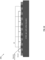
- Fig. 1A illustrates an example structure of the VCSEL 100.
- performance of VCSELs may be improved, particularly with respect to the modulation functions and/or characteristics thereof. In particular, this may be done by incorporating adjustments and/or additions to the structure of the VCSELs, which may yield improved performance without adding too much cost and/or complexity.
- the drive current may be modulated, which in turn modulates the output laser.
- the modulation of the VCSEL may be limited at times, by different factors including escape time of the photons from the cavity section of the VCSEL. While this lowering the gain may help, doing so still takes some time before photons may escape. This limits the speed of modulation in the VCSEL. Solutions in accordance with the present disclosure allow for modulation faster than photons escape time. This may be done by, e.g., re-directing the beams, to allow overcoming the photons escape time.
- an interdigitated grating may be used in the VCSEL, as illustrated in Fig. 1A .
- the interdigitated grating may comprise metallic grating filled with Pockels material-that is, material having high Pockels coefficient material (e.g., Perkinamine TM for organic, KTO, etc.).
- the Pockels material may be selected based on predetermined selection criteria, such as ensuring that the high contrast grating allows for biasing the laser beams in the manner described herein.
- interdigitated gratings may allow for creating a "sub-lambda" (or “small with respect to distance to fiber") array of beams that may output the top of the modulator with destructive interference on the far-field, according with the Huygens-Fresnel principle. This leads to high (constructive) or low (destructive) power coupled into the fiber/in the far-field, such as by changing the applied bias between the two interdigitated gratings. As a second part, this effect may be enhanced by resonant effects, embedding this into the cavity.
- a high contrast grating (HCG) based approach may be used.
- HCGs may be used to replace the top distributed Bragg reflector (DBR) layer of the vertical-cavity surface-emitting laser (VCSEL).
- DBR distributed Bragg reflector
- VCSEL vertical-cavity surface-emitting laser
- any suitable high contrast grating (HCG) based design allowing for achieving the required increase in modulation speed, may be used.
- key considerations when selecting and configuring the high contrast grating (HCG) structure used in the VCSEL, to enhance modulation performance thereof may be the ability to apply bias to the laser beams, applying gate tension, etc. For example, as shown in embodiment illustrated in Fig.
- the high contrast grating may comprise an etched structure, such as with an "in-plane” periodic or quasi-periodic structure of alternating low and high refractive index (RI), in order to achieve "out-of-plane” high reflectivities.
- contacts may be disposed on the top of the HCG structure (as shown in Fig. 1A ). These contacts may effectively function as a mirror.
- the contact may comprise metal or any suitable material.
- the HCG structure may incorporate some DBR material above the active layer/region.
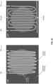
- a metallic array may be used, such as to connect, respectively, the contacts on the top of the surface of the HCG.
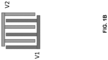
- Fig. 1B shows a top view of a metallic array as disposed on the top of the VCSEL.
- the metallic array may be used as interdigitated gates, with the etched high contrast grating (HCG) of the VCSEL being filled (e.g., in DOI: 10.1038/srep40348), with the holes filled with Pockels material.
- the Pockels material need not meet particular filling criteria (e.g., it may be used to fill the holes fully, but that may not be required).
- the Pockels coefficient of the material should allow for biasing the laser beams, such as to ensure creating destructive interferences and constructive interferences as described herein.
- the metal wires of the metallic array that is, the contacts on top of the HCG
- the metal wires of the metallic array may be connected to one another, and to V2, and may be insulated by a thin insulating layer.
- the Pockels material (paths) filling the holes of the HCG structure may be connected to one another, and to V1. Then, by applying a bias on V2, half of the paths may de-phased with respect to the second half, leading to destructive interferences.
- VCSEL photonic-crystal surface-emitting laser
- DFB distributed feedback polymer
- Fig. 2 illustrates an example vertical-cavity surface-emitting laser (VCSEL).
- VCSEL vertical-cavity surface-emitting laser
- VCSELs are commonly used as light (e.g., laser) sources, particularly in such implementations as transceivers (e.g., optical transceivers used in datacenters).
- VCSELs are driven using one or both of direct current ( I dc ) and alternating current ( I ac ).
- the VCSEL 200 comprises a multiple-quantum-well (MQW) layer, which functions as a gain medium, sandwiched between two mirrors (e.g., distributed Bragg reflector (DBR) layers). Further, VCSEL 200 comprises contacts, such as on the top side of the top mirror layer, and/or at the bottom side of the VCSEL 200.
- the contacts may comprise, e.g., metal material or the like.
- Fig. 3 illustrates an example photonic-crystal surface-emitting laser (PCSEL).
- PCSEL photonic-crystal surface-emitting laser
- PCSELs are commonly used as light (e.g., laser) sources, and are conventionally driven using one or both of direct current ( I dc ) and alternating current ( I ac ).
- the PCSEL 300 comprises a multiple-quantum-well (MQW) layer, which functions as gain medium, sandwiched between a mirror (e.g., distributed Bragg reflector (DBR)) layer on the bottom and a photonic crystal layer on the top of the MQW layer.
- MQW multiple-quantum-well
- DBR distributed Bragg reflector
- PCSEL 300 comprises contacts, such as on the top side of the top mirror layer, and/or at the bottom side of the PCSEL 300.
- the contacts may comprise, e.g., metal material or the like.
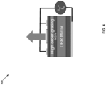
- Fig. 4 illustrates an example high-order distributed feedback polymer (DFB).
- a high-order distributed feedback polymer (DFB) 400 (or portion thereof).
- High-order DFBs are commonly used as light (e.g., laser) sources, and are conventionally driven using one or both of direct current ( I dc ) and alternating current ( I ac ).
- the high-order DFB 400 comprises a multiple-quantum-well (MQW) layer, which functions as gain medium, sandwiched between a mirror (e.g., distributed Bragg reflector (DBR)) layer on the bottom and a high-order grating layer on the top of the MQW layer.
- MQW multiple-quantum-well
- DBR distributed Bragg reflector
- the high-order DFB 400 comprises contacts, such as on the top side of the top mirror layer, and/or at the bottom side of the high-order DFB 400.
- the contacts may comprise, e.g., metal material or the like.
- Fig. 5A illustrates an example vertical-cavity surface-emitting laser (VCSEL) based electro-absorption modulated laser (EML), in accordance with the present disclosure.
- VCSEL vertical-cavity surface-emitting laser
- EML electro-absorption modulated laser
- the VCSEL-EML 500 comprises a multiple-quantum-well (MQW) layer, which functions as gain medium, sandwiched between two mirrors (e.g., distributed Bragg reflector (DBR) layers), with an electro-absorption modulated laser (EML) based structure on top side of the top mirror layer.
- MQW multiple-quantum-well
- DBR distributed Bragg reflector
- EML electro-absorption modulated laser
- VCSEL-EML 500 may comprise contacts, such as on the top side of the EML based structure, on the top side of the top mirror layer, and/or at the bottom side of the VCSEL-EML 500.
- the contacts may comprise, e.g., metal material or the like.
- VCSELs are commonly used as light (e.g., laser) sources, particularly in such implementations as transceivers (e.g., optical transceivers used in datacenters).
- transceivers e.g., optical transceivers used in datacenters.
- direct-drive or DAC/DC based VCSELs are used.
- directly modulated VCSELs are getting very close to a bandwidth (BW) bottleneck, between electrical and optical bandwidth.
- BW bandwidth
- VCSEL-EML devices are used, where an EML based structure is added, for use in handling at least some of modulation performed in the VCSEL.
- a modulating voltage may be applied across the EML based structure, and a current is then provided to drive the device as a whole.
- the device may be driven using a time-varying voltage, which allows for digitized based driving (e.g., based on the voltage on or off), such as a digital signal that modulates the output light signal.
- the device can be driven by direct current (DC) so it is always on.
- DC direct current
- performance of VCSEL-EMLs may be improved and/or optimized, particularly by modifying the EML based structure used therein.
- VCSEL-EMLs may be modified to implement a new modulation scheme, such as by incorporating a vertical EML that uses and/or takes advantage of the Pockels effect.
- the VCSEL may be used as a continuous waveform (CW) light source, with the proposed EML based structure monolithically implemented on top of the VCSEL's top mirror (e.g., DBR) layer.
- the EML may be modified, to improve performance of the EML and the device as a whole, particularly by incorporating Pockels material to make use of the Pockels effect.
- the Pockels effect is a directionally-dependent linear variation in the refractive index (RI) of an optical medium that occurs in response to the application of an electric field.
- the refractive index of an optical medium is a dimensionless number that gives the indication of the light bending ability of that medium.
- the refractive index is an indication of speed of light in the material.
- Pockels material is added into the EML based structure to enable (e.g., by controlling applying of voltage across the Pockels material) modulating light based on the material's refractive index (RI), which in turn affects behavior of light beams when applied to the EML based structure.
- Such approach may be material agnostic-e.g., utilizing instead adaptation of a bias scheme on top of the EML based structure.
- the Pockels material used in the EML may be selected and/or applied adaptively to ensure that particular performance criteria are met (e.g., as determined in terms of desired or required RI), as described herein.
- the added Pockels material may be used in conjunction with a bias scheme (applicable to the EML based structure), with the bias scheme being adapted for the desired modulation functions.
- the VCSEL-EML 500 is implemented as an integrated 3-contact VCSEL with laser-DC drive separated from the modulation drive. This allows use of an EML electronic scheme, with a direct-drive of the modulation part. Incorporating Pockels material into the EML based structure allows for improvement in performance based on adaptive use of the Pockels effects. In particular, the Pockels material may be utilized to enable forming and/or utilizing subwavelength patterns to enhance the Pockels effect.
- the EML may incorporate gratings configured to support the modulation functions, with these gratings incorporating Pockels material to make use of the Pockels effect.
- incorporating Pockels material may be done in conjunction with use of high contrast gratings (HCG).
- HCG high contrast gratings
- use of high contrast gratings (HCG) may be desirable as it may offer various advantages, such as limited optical losses (e.g., ⁇ 3dB), ability to use high Pockels material, ability to use readily available simulation capabilities of HCG, etc.
- etching structures in a high index material e.g., 50-100 nm wide, and 200-400 nm deep
- a high index material e.g., 50-100 nm wide, and 200-400 nm deep
- the proposed EML based structure may be used to provide various modulation functions.
- the EML may be used to modulate the output power (intensity modulation or amplitude modulation), to modulate the deflection of the beam-e.g., output coupling into the fiber (wavefront modulation), and/or to modulate the polarization of the beam (polarization modulation).
- the proposed EML based structure may be configured to meet particular performance criteria.
- the EML may have target V ⁇ ⁇ 5V.
- Meeting such performance criteria may require designing and/or configuring the EML based structure accordingly.
- ensuring meeting such target V ⁇ may require, e.g., optical field enhancement in Pockels material.
- the proposed EML based structure may be utilized in other applications, such as for providing 100s Gbps components (e.g., passive optical network (PON) elements (on fiber tips, vertical modulator/couplers, etc.), MUX/DEMUX functions, etc.), for beam steering (e.g., as ultra-fast spatial light modulator), and the like.
- PON passive optical network
- MUX/DEMUX functions etc.
- beam steering e.g., as ultra-fast spatial light modulator
- the proposed EML based structure may be used in conjunction with a photonic-crystal surface-emitting laser (PCSEL) light source (rather than VCSEL).
- PCSEL photonic-crystal surface-emitting laser
- the use of a PCSEL as a light source may be beneficial-e.g., optimizing benefits from HCG design possibilities.
- a PCSEL may be an optimal light source as it is an intrinsically single mode device, may allow for leveraging the full potential of High Q resonance of the HCG, and/or may allow for uniform illumination of HCG (which allows for avoiding detrimental finite size effects of HCG).
- Fig. 5B illustrates an example 3-contacts vertical-cavity surface-emitting laser (VCSEL) based electro-absorption modulated laser (EML), in accordance with the present disclosure.
- VCSEL vertical-cavity surface-emitting laser
- EML electro-absorption modulated laser
- the VCSEL-EML 520 may be substantially similar to the VCSEL-EML 500 of Fig. 5A , and may operate in a substantially manner.
- the VCSEL-EML 520 comprises an electro-absorption modulated laser (EML) based structure on top of a generic vertical emitting laser structure.
- the generic vertical emitting laser structure may comprise any suitable structure that may be configured to enable emitting a laser vertically.
- the generic vertical emitting laser structure may have a similar structure as the corresponding structure in the VCSEL-EML 500 of Fig. 5A , and as such may comprise a multiple-quantum-well (MQW) layer, which functions as a gain medium, sandwiched between two mirrors (e.g., distributed Bragg reflector (DBR) layers).
- MQW multiple-quantum-well
- VCSEL-EML 520 may comprise contacts, such as on the top side of the EML based structure, on the top side of the generic vertical emitting laser structure, and/or on the bottom side of the generic vertical emitting laser structure.
- the contacts may comprise, e.g., metal material or the like.
- the VCSEL-EML 520 represents an alternative design that utilizes 3 contacts.
- the 3 contacts may correspond to, respectively, the contact(s) on the top side of the EML based structure, the contact(s) on the top side of the generic vertical emitting laser structure, and the contact(s) on the bottom side of the generic vertical emitting laser structure. These 3 contacts are driven using I dc and/or V ac .
- Fig. 5C illustrates an example 4 contacts vertical-cavity surface-emitting laser (VCSEL) based electro-absorption modulated laser (EML), in accordance with the present disclosure.
- VCSEL vertical-cavity surface-emitting laser
- EML electro-absorption modulated laser
- the VCSEL-EML 540 may be substantially similar to the VCSEL-EML 500 of Fig. 5A , and may operate in a substantially manner.
- the VCSEL-EML 540 comprises an electro-absorption modulated laser (EML) based structure on top of a generic vertical emitting laser structure, with an electrical insulating layer in-between.
- the generic vertical emitting laser structure may comprise any suitable structure that may be configured in emitting laser vertically.
- the generic vertical emitting laser structure may have a similar structure as the corresponding structure in the VCSEL-EML 500 of Fig. 5A , and as such may comprise a multiple-quantum-well (MQW) layer, which functions as gain medium, sandwiched between two mirrors (e.g., distributed Bragg reflector (DBR) layers).
- MQW multiple-quantum-well
- VCSEL-EML 540 may comprise contacts, such as top side of the EML based structure, on the top side of the generic vertical emitting laser structure, and/or on the bottom side of the generic vertical emitting laser structure.
- the contacts may comprise, e.g., metal material or the like.
- the VCSEL-EML 540 represents an alternative design that utilizes 4 contacts.
- the 4 contacts may correspond to, respectively, the contact(s) on the top side of the EML based structure, the contact(s) on the top side of the generic vertical emitting laser structure, and the contact(s) on the bottom side of the generic vertical emitting laser structure, with the contacts on top of the EML based structure being configured into two separate groups of contacts, as shown in Fig. 5C .
- These 4 contacts are driven using I dc and/or V ac .
- Fig. 6 illustrates an example high contrast grating (HCG) structure, in accordance with the present disclosure.
- VCSEL vertical-cavity surface-emitting laser
- HCG high contrast grating
- the VCSEL 600 comprises two mirrors with an active layer (e.g., MQW) sandwiched in-between, with the top mirror incorporating the HCG 610.
- a high contrast grating e.g., the HCG 610
- VCSEL vertical-cavity surface-emitting laser
- EML electro-absorption modulated laser
- gratings incorporate grating features with gaps therebetween, and may be characterized by such parameters as height of the grating features (dimension h), width of the grating features (dimension a), thickness of contact on top of the grating features (dimension h M ), period of the grating features-that is, distance between identical points in successive grating features (dimension d), and total depth of the gaps (combination of dimension h and h M , when contacts are disposed on top of grating features, as shown in Fig. 6 ).
- High contrast gratings such as the HCG 610, may incorporate grating features with subwavelength dimensions, and may have strong index contrast (e.g., in air index of grating > 1.7).
- the high contrast may be provided by the gaps, which may be filed (e.g., with air, which has very low RI), resulting in high contrast between the gaps and the grating structure features.
- the grating features are tall (and thus the gaps are deep). In other words, the gaps may be typically deeper than wide to observe specular effects.
- High contrast gratings such as the HCG 610, may exhibit two modes: reflection (mode 0) and transmission (mode 2), with an incident wave (from within the device-that is applied to the HCG from below, after propagating through the underlying substrate) being reflected in mode 0, and passing (as output wave) in mode 2, as shown in Fig. 6 (in graph 620).
- the reflection/transmission modes may be coupled to each other and plane waves.
- high contrast gratings may have two essential features: 1) that only few modes may be excited and out-coupled as "plane wave” from the outside, and 2) that modes may get squeezed in space, getting higher transverse momentum.
- HCG cuts high spatial frequency components.
- 2 or 3 modes description of HCG is enough to predict general behavior, with another mode being usually evanescent.
- such other mode(s) may lay below the cone of light, and may enter 2 nd order when estimating the reflection/transmission properties at HCG interface with air.
- propagation constant is reduced, and destructive interference between the modes may be obtained (e.g., for structure at ⁇ -wavelength).
- the high contrast gratings may exhibit different performance characteristics at different wavelength ranges. For example, for subwavelength dimensions, only one mode may exist in the structure, and with increasing HCG thickness, Fabry-Perot (FP) nodes/antinodes may be seen. For the super-wavelength dimensions many modes may exist, with periodic recovery of the input signal in manner/pattern similar to the Talbot effect. In between these two ranges, few modes may exist. Further, at specific locations the two modes may simultaneously resonant in the HCG. For example, with 2n ⁇ phase difference energy may be trapped inside the HCG, and there may be large field enhancement (e.g., 1e3), and may manifest as anti-crossing. With (2n+1) ⁇ phase difference, part of the energy may be reflected back from HCG.
- 2n ⁇ phase difference energy may be trapped inside the HCG, and there may be large field enhancement (e.g., 1e3), and may manifest as anti-crossing. With (2n+1) ⁇ phase difference, part of the energy may be reflected back from HCG
- High contrast gratings may also be used in other applications, such as beam manipulation (e.g., lens, polarization, diffractive elements), wave guiding (e.g., MMI, spot size converter, etc.), high broadband reflectivity, broadband AR coating, non-linear optics, bio or chemical sensing, etc.
- beam manipulation e.g., lens, polarization, diffractive elements
- wave guiding e.g., MMI, spot size converter, etc.
- high broadband reflectivity e.g., broadband AR coating, non-linear optics, bio or chemical sensing, etc.
- Pockels material may be incorporated into the HCG structure-e.g., by using Pockels material to fill at least some of the gaps between the grating features and/or to form the grating features (e.g., with the contacts on top).
- use of Pockels material may allow for improving operation of the HCG structure, particularly with respect to modulation functions thereof. This is described in more detail below.
- Fig. 7 illustrates use of an example high contrast grating (HCG) structure as reflectivity modulator, in accordance with the present disclosure.
- a vertical-cavity surface-emitting laser (VCSEL) 700 incorporating a high contrast grating (HCG).
- the VCSEL 700 may correspond to a vertical-cavity surface-emitting laser (VCSEL) based electro-absorption modulated laser (EML) implemented based on the present disclosure, with the HCG being used in the proposed EML based structure for facilitating and/or supporting the modulation functions performed thereby. Illustrated in Fig. 7 is an application of HCG-namely, use of HCG in an EML based structure operating as a reflectivity modulator.
- VCSEL vertical-cavity surface-emitting laser
- EML electro-absorption modulated laser
- Such reflectivity modulator may exhibit high field enhancement.
- grating that uses silicon, there may be 30x field enhancement at 2V "V ⁇ ".
- various aspects or features may be modified to further enhance performance.
- dimerized-HCG may be used (rather than regular HCG) for better control.
- different material may be used in the grating structure, such as by using BaTiO3 or organic material instead of silicon, which may yield higher tunability.
- reflectivity modulation may be further enhanced by incorporating Pockels material into the HCG structure-e.g., within the gaps between the features (etchings), by using the Pockels material to form the features (with the contacts on top), etc.
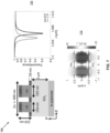
- Fig. 8 illustrates use of an example high contrast grating (HCG) structure in wavefront modulation, in accordance with the present disclosure.
- HCG high contrast grating
- the HCG 800 may be used with a vertical-cavity surface-emitting laser (VCSEL) based electro-absorption modulated laser (EML) implemented based on the present disclosure, with the HCG being used in the proposed EML based structure for facilitating and/or supporting the modulation functions performed thereby. Illustrated in Fig. 8 is an application of HCG-namely, use of HCG 800 in an EML based structure operating as a wavefront modulator.
- VCSEL vertical-cavity surface-emitting laser
- EML electro-absorption modulated laser
- the HCG may be biased by group-that is, sets of gratings in the HCG structure, as illustrated in Fig. 8 .
- Such biasing allows for deflecting the beam to discrete angle(s).
- the angle(s) may be defined by, e.g., the discrete geometry of the HCG structure.
- the angle(s) of deflection (or diffraction for external incident beams) may be tunable, as illustrated in Fig. 8 (810) and captured in graph 820 showing normalized angular intensity distribution based on use of an example proposed EML based structure.
- wavefront modulation may be further enhanced by incorporating Pockels material into the HCG structure-e.g., within the gaps between the features (etchings), by using the Pockels material to form the features (with the contacts on top), etc.
- Fig. 9 illustrates use of an example vertical-cavity surface-emitting laser (VCSEL) based electro-absorption modulated laser (EML) incorporating high contrast grating (HCG) with Pockels material as an intensity modulator, in accordance with the present disclosure.
- VCSEL vertical-cavity surface-emitting laser
- EML electro-absorption modulated laser
- HCG high contrast grating
- FIG. 9 there is shown a high contrast grating (HCG) 900.
- a high contrast grating may be utilized in a vertical-cavity surface-emitting laser (VCSEL) based electro-absorption modulated laser (EML) implemented based on the present disclosure, with the HCG 900 being configured for such use in the proposed EML based structure for facilitating and/or supporting the modulation functions performed thereby.
- VCSEL vertical-cavity surface-emitting laser
- EML electro-absorption modulated laser
- the HCG 900 may incorporate two contacts, which may be arranged in an interleaved manner (as shown in the plan view-that is, looking down onto the top of structure) thus forming an interdigitated grid of gates.
- the HCG 900 may also comprise Pockels material.
- the Pockels material is used to fill the gaps between the two contacts.
- the disclosure is not limited to such approach, however, and as such the arrangement of contacts and/or disposition of Pockels material may be done in any suitable manner.
- an alternative design is illustrated in Fig. 13 , with the contacts laid on top of the Pockels material.
- V1 and V2 Separate voltages may be applied to the two contacts to create particular bias in the HCG.
- the interdigitated grid allows for creating electric fields through the Pockels material between the two different grating elements (corresponding to where V1 and V2 are applied to the contacts).
- the two contacts are not (necessarily) made of different material; rather, applying different voltages to the contacts creates the different electric fields.
- the Interdigitated bias grid creates transverse electric field(s), as shown in Fig. 9 -that is, due to the interleaved arrangement, the direction of the electric field across the Pockels material may alternate (as shown).
- the interdigitated bias grid may also periodically modify the refractive index (RI) of the HCG structure as a whole.
- the RI may be modified in the grating by changing the electric field(s) applied across the Pockels material. Because the RI governs speed of light, modifying the RI alters the phase of the light passing through the grating.
- Pockels material may further enhance performance.
- Pockels material and Pockels effect corresponding thereto
- the Pockels effect by itself may be too small to achieve a desired ⁇ phase change, and as such resonance may be also used to achieve required optical field enhancement.
- achieving the desired Pockels effect may be achieved by providing resonance field enhancement rather than by increasing voltage.
- the resonance from the grating structure may be used to increase the strength of the optical field, and thereby enhance the Pockels effect (without increasing the voltage applied to the grating).
- the use of HCG in the proposed EML based structures may allow for achieving low target V ⁇ (e.g., ⁇ 5V).
- V ⁇ e.g., ⁇ 5V
- the angle of the tilt ( ⁇ ) may be determined using the formula: sin ⁇ ⁇ n 2 ⁇ Vr 33 h d 2 where h is the height of the material, and d the grating period. Without field enhancement, the effect may be too small.
- HCG High Contrast gratings
- an EML based structure (e.g., used in VCSEL-EML devices) incorporating the HCG 900 may function as an intensity (amplitude) modulator.
- the EML based structure may also be used to provide other functions, such as wavefront modulation, reflectivity modulation, etc.
- EML based structures e.g., used in VCSEL-EML devices
- HCG incorporating Pockels material may be utilized in providing polarization rotation.
- the grating features are inherently linear polarizers, and thus will selectively transmit optical beams having polarizations in a particular direction (e.g., x-direction).
- the structure may be configured to provide polarization rotation, which may be used in, e.g., blocking beams. Use of polarization rotation in this manner may be in conjunction with or alternative to use of refractive index related features.
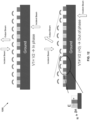
- Fig. 10 illustrates different processes for fabricating a vertical-cavity surface-emitting laser (VCSEL) based electro-absorption modulated laser (EML) incorporating high contrast grating (HCG) with Pockels material, in accordance with the present disclosure.
- VCSEL vertical-cavity surface-emitting laser
- EML electro-absorption modulated laser
- HCG high contrast grating
- FIG. 10 there are shown two different fabrication processes 1000 and 1010 for fabricating a VCSEL-EML having high contrast grating (HCG) structure with Pockels material.
- different methods may be used in fabricating optical devices (e.g., VCSEL) with EML based structures incorporating HCG with Pockels material, and the disclosure is not limited to a particular method or approach.
- the fabrication methods may differ with respect to the deposition technique used in applying the Pockels material.
- the fabrication methods also may be affected by the design of the HCG (e.g., with respect to the arrangement of the contacts used therein). For example, when using interdigitated contacts, there may be several physical implementations that may be used, as described in more detail below, and the fabrication methods may need to be adapted to account for use of such arrangement. As such, the fabrication methods may differ in the manner in which the Pockels material is applied in the particular grating (HCG) structure used.
- HCG grating
- the processes may be "Top bottom” or “Bottom up” depending on the deposition technique of Pockels material, as illustrated in Fig. 10 .
- a Pockels material layer is laid first on the insulating layer.
- the Pockels material layer is then etched to create space for the contacts, which are then added.
- the contacts are applied first on the insulating layer, with spaces therebetween based on pre-determined interleaved arrangement that comprises spaces between the contacts.
- the Pockels material layer is then deposited or formed into the spaces between the contacts.
- the processes used in fabricating the VCSEL-EML may be configured to meet pre-determined criteria (e.g., dimensions in the final structure, such as ⁇ 250 nm deep, openings in the 50-100 nm range, etc.
- fabricating the HCG structure involves addition and/or deposit of ⁇ 250 nm on the top to make the HCG, either only in particular areas (the spaces in the bottom up process), or on the whole surface with portion of the applied layer then removed (e.g., via the etching stop).
- the Pockels material-that is, applying it in the grating structure- may be done in various ways, and the disclosure is not limited to any particular approach, and as such any suitable approach may be utilized.
- the Pocket material may be implemented at wafer bonding level with processing (e.g., using BTO, Li.Nb., BaTiO3, etc.).
- the Pockels material may be implemented at the end the process, or toward the end (e.g., using organic, BTO based suspension, etc.).
- Fig. 11 illustrates dephasing in an example vertical-cavity surface-emitting laser (VCSEL) based electro-absorption modulated laser (EML) incorporating a high contrast grating (HCG) with Pockels material, in accordance with the present disclosure.
- VCSEL-EML 1100 incorporating an HCG structure with Pockels material within gaps between the contacts.
- the VCSEL-EML 1100 may be substantially similar to the VCSEL-EML 900 as described with respect to Fig. 9 .
- Illustrated in Fig. 11 is dephasing in VCSELs such as the VCSEL-EML 1100.
- dephasing may occur as a result of a voltage difference between the interdigitated gates, which may create a periodic change of refractive index (RI) in the structure.
- the RI may be modified by controlling (setting and/or changing) the electric field applied across the Pockels material. Because the RI governs speed of light, modifying the RI alters the phase of the light passing through the grating.
- dephasing may be done by adjusting the voltages applied to the two contacts.
- Fig. 12 illustrates use of an example vertical-cavity surface-emitting laser (VCSEL) based electro-absorption modulated laser (EML) incorporating a high contrast grating (HCG) with Pockels material in wavefront modulation, in accordance with the present disclosure.
- VCSEL-EML 1200 incorporating an HCG structure with Pockels material within gaps between the contacts.
- the VCSEL-EML 1200 may be substantially similar to the VCSEL-EML 900 as described with respect to Fig. 9 . As illustrated in Fig. 12 , the VCSEL-EML 1200 may function as a wavefront modulator.
- the refractive index (RI) may be modified based on changing the electric field applied across the Pockels material onto the different contacts. As noted, RI governs speed of light, and thus modifying the RI alters the phase of the light passing through the grating. Accordingly, the contacts are in phase when the Pockels material is subjected to the same voltage, and are out of phase when the voltages are different, as shown in Fig. 12 .
- ⁇ -wavelength gratings may share the same bias. This allows the output wave to stay in the light cone, while creating a dephasing between groups or grating.
- a Pockels-based EML e.g., such as the VCSEL-EML 1200 of Fig. 12
- a wavefront modulator may be restricted to only certain types of Pockels material. For example, only Pockels material with strong r42 may be used.
- Fig. 13 illustrates use of an example vertical-cavity surface-emitting laser (VCSEL) based electro-absorption modulated laser (EML) incorporating a high contrast grating (HCG) with contacts on top of the Pockels material in wavefront modulation, in accordance with the present disclosure.
- VCSEL-EML 1300 incorporating an HCG structure with Pockels material.
- the VCSEL-EML 1300 may be substantially similar to the VCSEL-EML described with respect to Fig. 9 . However, the VCSEL-EML 1300 may differ in that the contacts are disposed on top of the Pockels material, as shown in Fig. 13 . As illustrated in Fig. 13 , the VCSEL-EML 1300 may function as wavefront modulator. In this regard, the VCSEL-EML 1300, when used as wavefront modulator, may operate in substantially similar manner as the VCSEL-EML 1200, as described with respect to Fig. 12 .
- the refractive index (RI) may be also modified in the VCSEL-EML 1300 based on changing the electric field applied across the Pockels material-however, the electric field is applied here from the substrate through the Pockels material onto the contacts on top of the Pockels material.
- modifying the RI alters the phase of the light passing through the grating, with the contacts being in phase when subjected to the same voltage, and out of phase when the voltages are different, as shown in Fig. 13 .
- Fig. 14 illustrates handling of incoming external light in an example vertical-cavity surface-emitting laser (VCSEL) based electro-absorption modulated laser (EML) with a high contrast gratings (HCG) structure incorporating Pockels material, in accordance with the present disclosure.
- VCSEL-EML 1400 incorporating an HCG structure with Pockels material within gaps between the contacts.
- the VCSEL-EML 1400 may be substantially similar to the VCSEL-EML 900 as described with respect to Fig. 9 .
- the high contrast gratings (HCG) structure in the VCSEL-EML 1400 may comprise different material, such as Aluminum Gallium Arsenide (AlGaAs).
- AlGaAs Aluminum Gallium Arsenide
- Such design may have various benefits, such as being small, being superfast, having low losses, allowing for wavelength tuning by the grating rather than the material (e.g., Coarse Wavelength Division Multiplexing (CWDM) or Dense Wavelength Division Multiplexing (DWDM) on the same array).
- Use of an external laser source e.g., comb-laser
- Illustrated in Fig. 14 is handling of an incoming beam (light) projected onto the VCSEL-EML 1400 from the outside (rather than from the bottom, through the substrate).
- the absorption resonance of the HCG in the VCSEL-EML 1400 may be tweaked, leading to a change of reflectivity.
- the contact would be out of phase, resulting in the incoming light be reflected back at a particular angle, as shown in Fig. 14 .
- Fig. 15 illustrates use of an example vertical-cavity surface-emitting laser (VCSEL) based electro-absorption modulated laser (EML) incorporating high contrast grating (HCG) with Pockels material in polarization modulation, in accordance with the present disclosure.
- VCSEL-EML 1500 there is shown VCSEL-EML 1500.
- the VCSEL-EML 1500 may be substantially similar to the VCSEL-EML described with respect to Fig. 9 . However, the VCSEL-EML 1500 may differ in that the contacts (e.g., metal contacts) are disposed on top of the Pockels material, as shown in Fig. 15 . As illustrated in Fig. 15 , the VCSEL-EML 1500 may function as polarization modulator. Nonetheless, polarization modulation as described herein is not limited the particular implementation corresponding to the VCSEL-EML 1500, and such polarization modulation may be applicable to and/or provided by any of the proposed EML based structures disclosed herein.
- the HCG may have strong birefringence between transverse electric (TE) and transverse magnetic (TM) modes.
- the design and/or implementation of the device may be adapted to utilize such characteristics in providing polarization modulation via the proposed EML based structures (incorporating Pockels material). This may be doable for any of the implementations disclosed herein.
- the polarization modulation may be provided by taking advantage of, e.g., the interdigitated contact arrangements in the proposed EML structures.
- the same principles and approach used in wavefront modulation may be used for polarization modulation-e.g., by connecting all the teeth of HCG to the same bias source.
- the polarization modulation may be viewed as a subset of amplitude modulation schemes.
- polarization modulation may be achieved by applying modulation to allow or suppress modes inside the HCG.
- HCG properties may change specularly in the vicinity of mode cutoff(s), as illustrated in graphs 1510 and 1520, which show abrupt changes for TE-reflectivity and abrupt changes for TM-reflectivity, as well as regions of overlapping.
- overlapping transitions frequencies e.g., for TM6/TE6
- the EML structure may be modified to optimize polarization modulation.
- the appropriate thickness of HCG may allow for identifying spot(s) where TE reflectivity increases as TM reflectivity decreases (or vice versa) when changing bias.
- Fig. 16 illustrates example variations of high contrast grating (HCG) structures with Pockels material, in accordance with the present disclosure.
- HCG high contrast grating
- FIG. 16 there are shown various variations of HCG with Pockels material.
- HCGs 1600, 1610, 1620, 1630, 1640, and 1650 are shown in Fig. 16.
- HCG 1600 represent the base implementation
- HCGs 1610, 1620, 1630, 1640, and 1650 represent alternative variations of the base implementation.
- Variations from the base implementation may comprise dimerized versions of HCG.
- lower resonance frequency may be possible with such variations.
- Such variations may be of different flavors. For example, this may be done by changing the geometrical parameters, such as width of the high or low index material, as illustrated in HCG 1640 (variation 1), by changing material every second teeth, as illustrated in HCG 1640 (variation 2), or by connecting every 2 nd tooth, as illustrated in HCG 1640 (variation 3).
- Patterns of the HCG also may be varied spatially-e.g., based on changes in the pattern in x- or y-directions. This may include a slow shift of the resonance with the space-e.g., less than 1% variation over lambda, as illustrated in HCG 1640 (variation 4), or an abrupt shift of HCG parameters-e.g., one or more parameter have 1 % variation between one repetition of the motif and the next, but the geometry is stable over more than 10 lambda, as illustrated in HCG 1640 (variation 5).
- FIG. 17 illustrates a first example implementation of an interdigitated electro-absorption modulated laser (EML) based structure, in accordance with the present disclosure.
- EML electro-absorption modulated laser
- the EML based structure 1700 comprises a generic vertical emitting layer followed (in the z-direction), that is, topped, by insulating layer(s), and then a high contrast grating (HCG) that comprises two contacts (V1 and V2) comprising semiconductor (e.g., doped semiconductor) material with metal on top, with Pockels material disposed in-between the contacts.
- HCG high contrast grating
- the contacts are covered (optionally) by a capping layer (which is not shown in the top view 1710).
- the generic vertical emitting layer may comprise any suitable structure that may be configured in emitting a laser vertically.
- the generic vertical emitting layer may comprise a substrate, which may be optionally sandwiched between two vertical emitting epi-stack layers.
- the epi-stack may comprise a VCSEL or PCSEL (or 2 nd , 3 rd , ... , n th order distributed-feedback laser (DFB)).
- the substrate may comprise suitable material, such as gallium arsenide (GaAs), gallium nitride (GaN), indium phosphide (InP), silicon (Si), silicon carbide (SiC), or the like.
- the insulating layer may comprise semiconductor (doped or undoped current blocking layer), or ceramics (aluminum oxide AlO x , silicon nitride (SiN), silicon oxide (SiO2), etc.).
- the Pockels material may comprise large r33 material.
- the metal used in the contacts may comprise gold (Au), silver (Ag), copper (Cu), or transparent conducting materials (e.g., like indium tin oxide (ITO), or the like).
- the Pockels material used in this implementation may need to have low refractive index (e.g., IR ⁇ 2), such as a polymer.
- low refractive index e.g., IR ⁇ 2
- the balance between optical losses and RF electrical losses depends on exact application.
- the vertical emitting epi stack layer(s) may or may not be included, either between substrate and the EML, or below the substrate.
- FIG. 18 illustrates a second example implementation of an interdigitated electro-absorption modulated laser (EML) based structure, in accordance with the present disclosure.
- EML electro-absorption modulated laser
- the EML based structure 1800 comprises generic vertical emitting layer followed (in the z-direction), that is, topped, by insulating layer(s), and then a high contrast grating (HCG) that comprises two contacts (V1 and V2) with Pockels material disposed in-between the contacts.
- HCG high contrast grating
- the contacts are covered (optionally) by a capping layer (which is not shown in the top view 1810).
- the generic vertical emitting layer may comprise any suitable structure that may be configured to enable emitting a laser vertically.
- the generic vertical emitting layer may comprise a substrate, which may be optionally sandwiched between two vertical emitting epi-stack layers.
- the epi-stack may comprise a VCSEL or PCSEL (or 2 nd , 3 rd , ... , n th order Distributed-feedback laser (DFB)).
- the substrate may comprise suitable material, such as gallium arsenide (GaAs), gallium nitride (GaN), indium phosphide (InP), silicon (Si), silicon carbide (SiC), or the like.
- the insulating layer may comprise semiconductor (doped or undoped current blocking layer), or ceramics (aluminum oxide AlO x , silicon nitride (SiN), silicon oxide (SiO 2 ), etc.).
- the Pockels material may comprise large r33 material.
- the contacts (V1 and V2) may comprise transparent metal with low index n ⁇ 1.6 (e.g., silver nanowire (AgNW), CN, hybrids, or the like).
- the Pockels material used in this implementation may need to have high refractive index >2 (e.g., SBN60, BaTi03, etc.). Further, as with the prior implementations, the vertical emitting epi stack layer(s) may or may not be included, disposed either between substrate and the EML, or below the substrate.
- FIG. 19 illustrates a third example implementation of an interdigitated electro-absorption modulated laser (EML) based structure, in accordance with the present disclosure.
- EML electro-absorption modulated laser
- the EML based structure 1900 comprises generic vertical emitting layer followed (in the z-direction)-that is, topped-by a lateral contact layer, and then a high contrast grating (HCG) that comprises two contacts (V1 and V2) comprising semiconductor (e.g., doped semiconductor) material with metal on top, with Pockels material disposed in-between the contacts metal on top of Pockels material, with undoped semiconductor material disposed in-between the contacts-particularly the Pockels material thereof, as shown.
- the contacts are covered (optionally) by a capping layer (which is not shown in the top view 1910).
- the generic vertical emitting layer may comprise any suitable structure that may be configured to enable emitting a laser vertically.
- the generic vertical emitting layer may comprise a substrate, which may be optionally sandwiched between two vertical emitting epi-stack layers.
- the epi-stack may comprise a VCSEL or PCSEL (or 2 nd , 3 rd , ... , n th order Distributed-feedback laser (DFB)).
- the substrate may comprise suitable material, such as gallium arsenide (GaAs), gallium nitride (GaN), indium phosphide (InP), silicon (Si), silicon carbide (SiC), or the like.
- the lateral contact layer may comprise transparent and electrically conductive material.
- the Pockels material may comprise large r42, 63, etc., Pockels material.
- the metal of the contacts may comprise gold (Au), silver (Ag), copper (Cu), or transparent conducting materials (e.g., like indium tin oxide (ITO), or the like).
- the Pockels material used in this implementation may need to have low refractive index (e.g., IR ⁇ 2), such as KDP, polymer, etc.
- the vertical emitting epi stack layer(s) may or may not be included, either between a substrate and the EML, or below the substrate.
- FIG. 20 illustrates fourth and fifth example implementations of an interdigitated electro-absorption modulated laser (EML) based structure, in accordance with the present disclosure.
- EML electro-absorption modulated laser
- each of the EML based structures 2000 and 2010 comprises generic vertical emitting layer followed (in the z-direction), that is, topped, by a lateral contact layer, and then a high contrast grating (HCG) that comprises two contacts (V1 and V2) comprising semiconductor (e.g., doped semiconductor) material with metal on top, with contact metal on top of the Pockels material, with undoped semiconductor material disposed in-between the contacts-particularly the Pockels material thereof, as shown.
- the contacts are covered (optionally) by a capping layer (which is not shown in the top view 2010).
- the generic vertical emitting layer may comprise any suitable structure that may be configured to enable emitting a laser vertically.
- the generic vertical emitting layer may comprise a substrate, which may comprise emitting epi-stack layers on either surface of the substrate.
- the epi-stack may comprise a VCSEL or PCSEL (or 2 nd , 3 rd , ... , n th order Distributed-feedback laser (DFB)).
- the substrate may comprise suitable material, such as gallium arsenide (GaAs), gallium nitride (GaN), indium phosphide (InP), silicon (Si), silicon carbide (SiC), or the like.
- the lateral contact layer may comprise transparent and electrically conductive material.
- the Pockels material may comprise large r42, 63, etc., Pockels material.
- the metal of the contacts may comprise gold (Au), silver (Ag), copper (Cu), or transparent conducting materials (e.g., like indium tin oxide (ITO), or the like).
- the EML based structures 2000 and 2010 may be substantially similar to the EML based structure 1900 as described with respect to Fig. 19 . However, the EML based structures 2000 and 2010 differ from one another (and from the EML based structure 1900) in that there are some variations in the HCG in each of these structures. In particular, the HCG of the EML based structure 2000 differs from the HCG of the EML based structure 2000 in that the contacts (V1 and V2) are of different size in the EML based structure 2000 (e.g., V1 is larger in V2, as shown in Fig. 20 ), whereas these contacts are the same size in the EML based structure 1900.
- the HCG used therein differs in that it incorporates capping layer material (in addition to the undoped semiconductor material) in-between the contacts, as shown in Fig. 20 .
- these two Implementations may exhibit similar physical effects as interdigitated EML based implementations because an effective refractive index varies differently in each dimer. In this regard, a similar effect may be obtained by, e.g., filling only about 1 ⁇ 2 of the HCG groves with Pockels materials, as shown in Fig. 20 .
- Fig. 21 illustrates a sixth example implementation of an interdigitated electro-absorption modulated laser (EML) based structure, in accordance with the present disclosure.
- EML electro-absorption modulated laser
- FIG. 21 there is shown an EML based structure 2100.
- a top view 2110 of the EML based structure 2100 is shown in Fig. 21, as well as a side view 2120 corresponding to particular cross section (line) in the structure.
- the EML based structure 2100 comprises generic vertical emitting layer followed (in the z-direction), that is, topped, by a lateral contact layer, and then a high contrast grating (HCG) that comprises two contacts (V1 and V2) comprising semiconductor (e.g., doped semiconductor) material, with metal on top of the Pockels material.
- HCG high contrast grating
- the contacts are covered (optionally) by a capping layer (which is not shown in the top view 2110).
- the capping material is also disposed in-between the contacts-particularly in-between the Pockels material thereof, as shown.
- the generic vertical emitting layer may comprise any suitable structure that may be configured to enable emitting a laser vertically.
- the generic vertical emitting layer may comprise a substrate, which may comprise emitting epi-stack layers on either surface.
- the epi-stack may comprise a VCSEL or PCSEL (or 2 nd , 3 rd , ... , n th order Distributed-feedback laser (DFB)).
- the substrate may comprise suitable material, such as gallium arsenide (GaAs), gallium nitride (GaN), indium phosphide (InP), silicon (Si), silicon carbide (SiC), or the like.
- the lateral contact layer may comprise transparent and electrically conductive material.
- the Pockels material may comprise large r42, 63, etc., Pockels material.
- the metal of the contacts may comprise gold (Au), silver (Ag), copper (Cu), or transparent conducting materials (e.g., like indium tin oxide (ITO), or the like).
- the vertical emitting epi stack layer(s) may or may not be included, either between substrate and the EML, or below the substrate.
- Fig. 22 illustrates an example vertical-cavity surface-emitting laser (VCSEL) based electro-absorption modulated laser (EML) incorporating high contrast grating (HCG) with Pockels material and with a dielectric for gates, in accordance with the present disclosure.
- VCSEL vertical-cavity surface-emitting laser
- EML electro-absorption modulated laser
- HCG high contrast grating
- VCSEL 2200 there is shown VCSEL 2200.
- the VCSEL 2200 may comprise a VCSEL epi layer (with no or few top pairs), with grating (e.g., HCG) structure on top having Pockels material filling the gaps within the grating structure, and with contacts on the top of the surface of the grating structure.
- Some of the contacts may incorporate dielectric (for the gate). As such some of the contacts (e.g., those lacking dielectric) may form and/or operate as ground whereas the remaining contact (e.g., those incorporating dielectric) may as the RF element in the VCSEL 2200.
- Fig. 23 illustrates example vertical-cavity surface-emitting laser (VCSEL) based optical devices with one incorporating electro-absorption modulated laser (EML) based design. Shown in Fig. 23 are optical devices 2300 and 2310, both of which are a VCSEL based device. In this regard, top view(s) of the optical devices 2300 and 2310 are shown in Fig. 23 .
- VCSEL vertical-cavity surface-emitting laser
- EML electro-absorption modulated laser
- the optical device 2300 comprises a VCSEL based structure (e.g., as described with respect to Fig. 2 ) on top of a substrate etching, with contact (wiring) on top of the VCSEL structure.
- the optical device 2300 may be configured to emit light (e.g., laser) in response to applying of RF in signal as input into contact wiring on one end, and outputting of a corresponding RF out/dump signal as output at the other end of the contact wiring.
- the optical device 2310 represents an example modification of the optical device 2300 in accordance with an example implementation based on the present disclosure.
- the optical device 2310 may be substantially similar to the optical device 2300, but may incorporate modification(s) to allow for providing the modulation functions and/or characteristics thereof as described herein.
- the optical device 2310 may incorporate modifications of the contact wirings, such as by use of multiple separate contact wirings, as illustrated in Fig. 23 , to form an interdigitated grating based design that allows for biasing of the contacts, as described above, such as by grounding (e.g., applying ground signal(s) into) some of the contact wirings as shown in Fig. 23 .
- "and/or” means any one or more of the items in the list joined by “and/or”.
- "x and/or y” means any element of the three-element set ⁇ (x), (y), (x, y) ⁇ .
- "x and/or y” means "one or both of x and y.”
- "x, y, and/or z” means any element of the seven-element set ⁇ (x), (y), (z), (x, y), (x, z), (y, z), (x, y, z) ⁇ .
- x, y and/or z means “one or more of x, y, and z.”
- exemplary means serving as a non-limiting example, instance, or illustration.
- terms "for example” and “e.g.” set off lists of one or more non-limiting examples, instances, or illustrations.
- circuits and “circuitry” refer to physical electronic components (e.g., hardware), and any software and/or firmware (“code”) that may configure the hardware, be executed by the hardware, and or otherwise be associated with the hardware.
- code software and/or firmware
- a particular processor and memory e.g., a volatile or non-volatile memory device, a general computer-readable medium, etc.
- a circuit may comprise analog and/or digital circuitry. Such circuitry may, for example, operate on analog and/or digital signals.
- a circuit may be in a single device or chip, on a single motherboard, in a single chassis, in a plurality of enclosures at a single geographical location, in a plurality of enclosures distributed over a plurality of geographical locations, etc.
- module may, for example, refer to a physical electronic component (e.g., hardware) and any software and/or firmware (“code”) that may configure the hardware, be executed by the hardware, and or otherwise be associated with the hardware.
- circuitry or module is "operable" to perform a function whenever the circuitry or module comprises the necessary hardware and code (if any is necessary) to perform the function, regardless of whether performance of the function is disabled or not enabled (e.g., by a user-configurable setting, factory trim, etc.).
- inventions may provide a non-transitory computer readable medium and/or storage medium, and/or a non-transitory machine readable medium and/or storage medium, having stored thereon, a machine code and/or a computer program having at least one code section executable by a machine and/or a computer, thereby causing the machine and/or computer to perform the processes as described herein.
- Computer program in the present context means any expression, in any language, code or notation, of a set of instructions intended to cause a system having an information processing capability to perform a particular function either directly or after either or both of the following: a) conversion to another language, code or notation; b) reproduction in a different material form.
Landscapes
- Physics & Mathematics (AREA)
- General Physics & Mathematics (AREA)
- Optics & Photonics (AREA)
- Condensed Matter Physics & Semiconductors (AREA)
- Electromagnetism (AREA)
- Nonlinear Science (AREA)
- Chemical & Material Sciences (AREA)
- Engineering & Computer Science (AREA)
- Ceramic Engineering (AREA)
- Crystallography & Structural Chemistry (AREA)
- Semiconductor Lasers (AREA)
- Optical Modulation, Optical Deflection, Nonlinear Optics, Optical Demodulation, Optical Logic Elements (AREA)
Priority Applications (1)
| Application Number | Priority Date | Filing Date | Title |
|---|---|---|---|
| EP24208431.7A EP4521569A1 (de) | 2023-08-15 | 2024-08-14 | Ultraschneller modulationsoberflächenemissionslaser mit vertikalem resonator (vcsel) |
Applications Claiming Priority (3)
| Application Number | Priority Date | Filing Date | Title |
|---|---|---|---|
| US202363532778P | 2023-08-15 | 2023-08-15 | |
| US202463575281P | 2024-04-05 | 2024-04-05 | |
| US18/802,317 US20250062596A1 (en) | 2023-08-15 | 2024-08-13 | Ultrafast modulation vertical-cavity surface-emitting laser (vcsel) |
Related Child Applications (2)
| Application Number | Title | Priority Date | Filing Date |
|---|---|---|---|
| EP24208431.7A Division EP4521569A1 (de) | 2023-08-15 | 2024-08-14 | Ultraschneller modulationsoberflächenemissionslaser mit vertikalem resonator (vcsel) |
| EP24208431.7A Division-Into EP4521569A1 (de) | 2023-08-15 | 2024-08-14 | Ultraschneller modulationsoberflächenemissionslaser mit vertikalem resonator (vcsel) |
Publications (2)
| Publication Number | Publication Date |
|---|---|
| EP4510397A2 true EP4510397A2 (de) | 2025-02-19 |
| EP4510397A3 EP4510397A3 (de) | 2025-03-12 |
Family
ID=92424367
Family Applications (2)
| Application Number | Title | Priority Date | Filing Date |
|---|---|---|---|
| EP24208431.7A Pending EP4521569A1 (de) | 2023-08-15 | 2024-08-14 | Ultraschneller modulationsoberflächenemissionslaser mit vertikalem resonator (vcsel) |
| EP24194522.9A Withdrawn EP4510397A3 (de) | 2023-08-15 | 2024-08-14 | Ultraschneller modulationsoberflächenemissionslaser mit vertikalem resonator (vcsel) |
Family Applications Before (1)
| Application Number | Title | Priority Date | Filing Date |
|---|---|---|---|
| EP24208431.7A Pending EP4521569A1 (de) | 2023-08-15 | 2024-08-14 | Ultraschneller modulationsoberflächenemissionslaser mit vertikalem resonator (vcsel) |
Country Status (4)
| Country | Link |
|---|---|
| US (1) | US20250062596A1 (de) |
| EP (2) | EP4521569A1 (de) |
| JP (1) | JP2025028026A (de) |
| CN (1) | CN119496039A (de) |
Family Cites Families (9)
| Publication number | Priority date | Publication date | Assignee | Title |
|---|---|---|---|---|
| JPS6032381A (ja) * | 1983-08-01 | 1985-02-19 | Matsushita Electric Ind Co Ltd | 面発光半導体レ−ザ装置 |
| JPH01105590A (ja) * | 1987-10-16 | 1989-04-24 | Toshiba Corp | 分布帰還型半導体発光素子 |
| US5301201A (en) * | 1993-03-01 | 1994-04-05 | At&T Bell Laboratories | Article comprising a tunable semiconductor laser |
| JP5104070B2 (ja) * | 2007-06-29 | 2012-12-19 | コニカミノルタホールディングス株式会社 | 2次元フォトニック結晶面発光レーザ |
| JP2015135395A (ja) * | 2014-01-17 | 2015-07-27 | パナソニックIpマネジメント株式会社 | 波長変換素子およびそれを用いた光源ランプ |
| CN107065233B (zh) * | 2017-03-21 | 2023-01-31 | 电子科技大学 | 一种基于亚波长高对比度光栅的电光可调滤波器 |
| US20210167580A1 (en) * | 2019-11-29 | 2021-06-03 | Pinnacle Photonics (Us), Inc. | Top emitting vcsel array with integrated gratings |
| US12149049B2 (en) * | 2020-12-31 | 2024-11-19 | Win Semiconductors Corp. | Vertical-cavity surface-emitting laser and method for forming the same |
| CN113054531B (zh) * | 2021-03-08 | 2022-04-29 | 苏州长光华芯光电技术股份有限公司 | 一种可调谐垂直腔面发射激光器及其制备方法 |
-
2024
- 2024-08-13 US US18/802,317 patent/US20250062596A1/en active Pending
- 2024-08-14 JP JP2024135408A patent/JP2025028026A/ja active Pending
- 2024-08-14 EP EP24208431.7A patent/EP4521569A1/de active Pending
- 2024-08-14 EP EP24194522.9A patent/EP4510397A3/de not_active Withdrawn
- 2024-09-19 CN CN202411309548.4A patent/CN119496039A/zh active Pending
Also Published As
| Publication number | Publication date |
|---|---|
| US20250062596A1 (en) | 2025-02-20 |
| EP4521569A1 (de) | 2025-03-12 |
| CN119496039A (zh) | 2025-02-21 |
| JP2025028026A (ja) | 2025-02-28 |
| EP4510397A3 (de) | 2025-03-12 |
Similar Documents
| Publication | Publication Date | Title |
|---|---|---|
| US9312663B2 (en) | Laser device, light modulation device, and optical semiconductor device | |
| US9240673B2 (en) | Tunable SOI laser | |
| EP1939653B1 (de) | Laser mit externem Resonator und einstellbarem resonanten Gitterfilter | |
| US8081850B2 (en) | Device with tunable plasmon resonance | |
| KR102037813B1 (ko) | 광 변조기 및 그를 구비한 광학 모듈 | |
| US9762025B2 (en) | Temperature insensitive integrated electro-absorption modulator and laser | |
| US20170317471A1 (en) | An optical device and a method for fabricating thereof | |
| JP5267105B2 (ja) | 光モジュール及びその製造方法、光送信器 | |
| KR102078573B1 (ko) | 분포 브라그 반사형 파장가변 레이저 다이오드 | |
| US10277008B1 (en) | Tunable laser device and method for manufacturing the same | |
| US8687665B1 (en) | Mutually injection locked lasers for enhanced frequency response | |
| JPH0964334A (ja) | 発光素子と外部変調器の集積素子 | |
| JP7334582B2 (ja) | 半導体光素子およびその製造方法 | |
| US20190013640A1 (en) | Tunable Laser | |
| CN107078459A (zh) | 包含光子晶体的外腔激光器 | |
| JP2025109711A (ja) | モノリシックに集積されたInPの電気光学的に調整可能なリングレーザー、レーザーデバイス、及び対応する方法 | |
| JP5171538B2 (ja) | 光変調器および波長可変レーザーモジュール | |
| EP4510397A2 (de) | Ultraschneller modulationsoberflächenemissionslaser mit vertikalem resonator (vcsel) | |
| JP2018060974A (ja) | 半導体光集積素子 | |
| US10243330B2 (en) | Optoelectronic device with resonant suppression of high order optical modes and method of making same | |
| JP6810671B2 (ja) | 半導体光集積素子 | |
| JP2014199882A (ja) | 光素子及び光モジュール | |
| EP4033618A1 (de) | Mach-zehnder-modulierte laser | |
| JP6299839B2 (ja) | 光素子及び光モジュール | |
| JP2013229357A (ja) | 分布帰還型半導体レーザ及びotdr装置 |
Legal Events
| Date | Code | Title | Description |
|---|---|---|---|
| PUAI | Public reference made under article 153(3) epc to a published international application that has entered the european phase |
Free format text: ORIGINAL CODE: 0009012 |
|
| STAA | Information on the status of an ep patent application or granted ep patent |
Free format text: STATUS: REQUEST FOR EXAMINATION WAS MADE |
|
| REG | Reference to a national code |
Ref country code: DE Ref legal event code: R079 Free format text: PREVIOUS MAIN CLASS: H01S0003097100 Ipc: H01S0005183000 |
|
| PUAL | Search report despatched |
Free format text: ORIGINAL CODE: 0009013 |
|
| 17P | Request for examination filed |
Effective date: 20240814 |
|
| AK | Designated contracting states |
Kind code of ref document: A2 Designated state(s): AL AT BE BG CH CY CZ DE DK EE ES FI FR GB GR HR HU IE IS IT LI LT LU LV MC ME MK MT NL NO PL PT RO RS SE SI SK SM TR |
|
| AK | Designated contracting states |
Kind code of ref document: A3 Designated state(s): AL AT BE BG CH CY CZ DE DK EE ES FI FR GB GR HR HU IE IS IT LI LT LU LV MC ME MK MT NL NO PL PT RO RS SE SI SK SM TR |
|
| RIC1 | Information provided on ipc code assigned before grant |
Ipc: H01S 5/42 20060101ALI20250206BHEP Ipc: H01S 5/183 20060101AFI20250206BHEP |
|
| P01 | Opt-out of the competence of the unified patent court (upc) registered |
Free format text: CASE NUMBER: APP_8701/2025 Effective date: 20250220 |
|
| STAA | Information on the status of an ep patent application or granted ep patent |
Free format text: STATUS: THE APPLICATION HAS BEEN WITHDRAWN |
|
| 18W | Application withdrawn |
Effective date: 20250715 |